Document Outline
- CS5320/21/22
- Features
- Description
- TABLE OF CONTENTS
- LIST OF FIGURES
- LIST OF TABLES
- Contacting Cirrus Logic Support
- 1. CHARACTERISTICS AND SPECIFICATIONS
- CS5320 AND CS5321 ANALOG CHARACTERISTICS
- Dynamic Performance
- dc Accuracy
- Input Characteristics
- Power Supplies
- CS5320 AND CS5321 SWITCHING CHARACTERISTICS
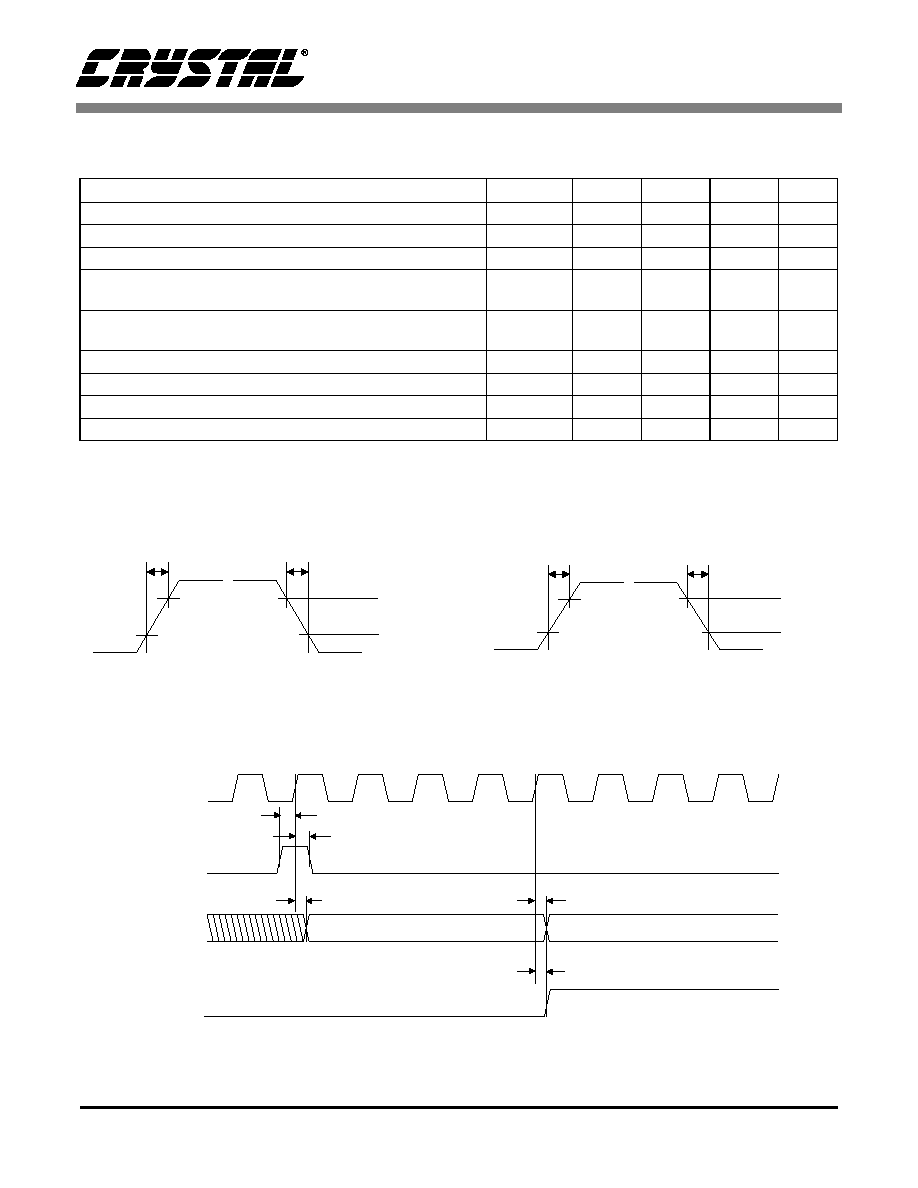
- Figure 1. Rise and Fall Times
- Figure 2. CS5320 and CS5321 Interface Timing, HBR=1
- CS5320 AND CS5321 DIGITAL CHARACTERISTICS
- CS5320 AND CS5321 RECOMMENDED OPERATION CONDITIONS
- CS5320 AND CS5321 ABSOLUTE MAXIMUM RATINGS
- CS5322 FILTER CHARACTERISTICS
- CS5322 POWER SUPPLY
- CS5322 SWITCHING CHARACTERISTICS
- CS5322 DIGITAL CHARACTERISTICS
- CS5322 RECOMMENDED OPERATION CONDITIONS
- CS5322 ABSOLUTE MAXIMUM RATINGS
- 2. GENERAL DESCRIPTION
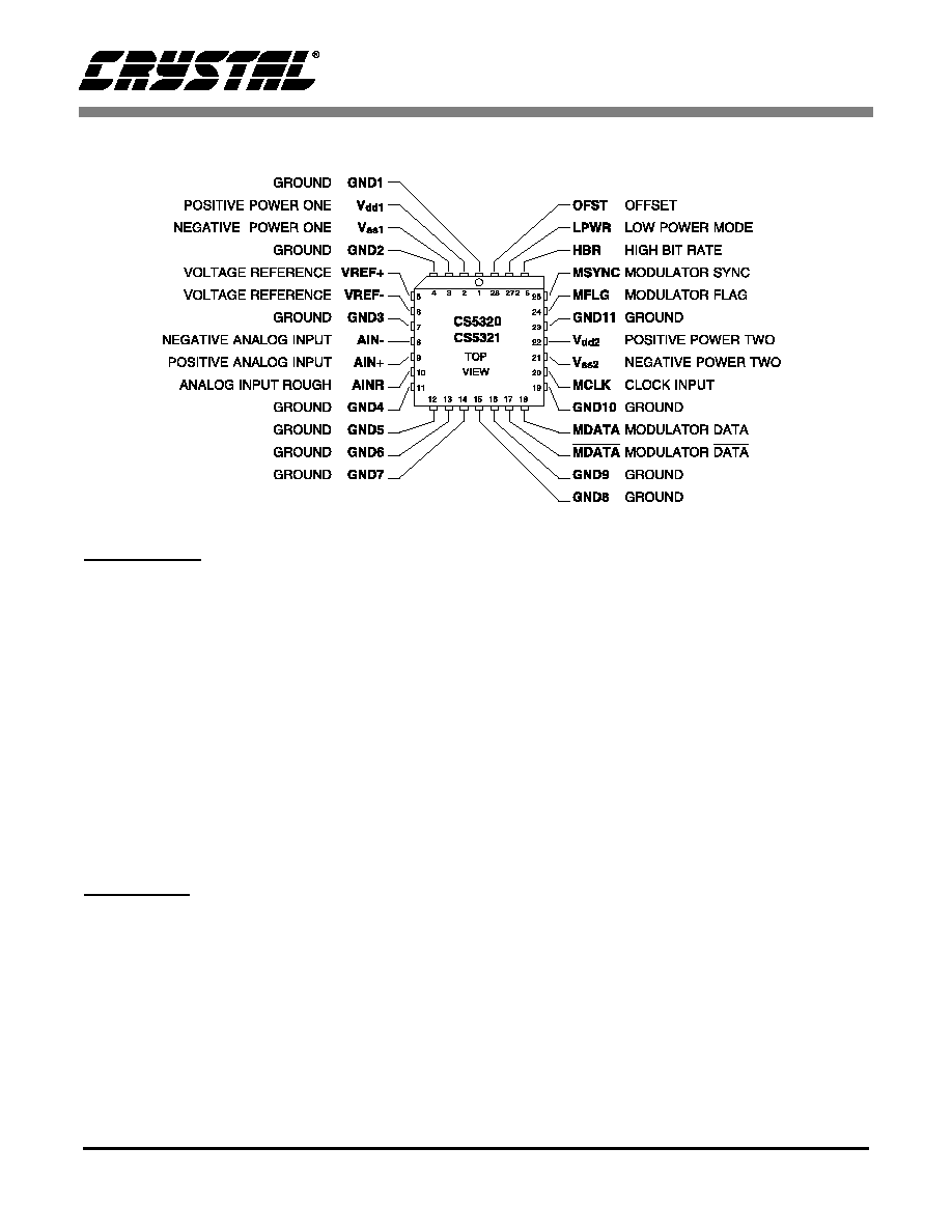
- 3. CS5320/21 PIN DESCRIPTIONS
- Pin Drawing
- Power Supplies
- Analog Inputs
- Digital Inputs
- Digital Outputs
- 4. CS5322 PIN DESCRIPTIONS
- Pin Drawing
- Power Supplies
- Digital Outputs
- Digital Inputs
- 5. ORDERING INFORMATION
- 6. PARAMETER DEFINITIONS
- 7. PACKAGE DIMENSIONS

Preliminary Product Information
This document contains information for a new product.
Cirrus Logic reserves the right to modify this product without notice.
1
Copyright
©
Cirrus Logic, Inc. 1999
(All Rights Reserved)
P.O. Box 17847, Austin, Texas 78760
(512) 445 7222 FAX: (512) 445 7581
http://www.cirrus.com
CS5320/21/22
24-Bit Variable Bandwidth A/D Converter Chipset
Features
l
CMOS A/D Converter Chipset
l
Dynamic Range
- 130 dB @ 25 Hz Bandwidth
- 121 dB @ 411 Hz Bandwidth
l
Delta-Sigma Architecture
- Fourth-Order Modulator
- Variable Oversampling: 64X to 4096X
- Internal Track-and-Hold Amplifier
l
CS5321 Signal-to-Distortion: 115 dB
l
Clock Jitter Tolerant Architecture
l
Input Voltage Range: +4.5 V
l
Flexible Filter Chip
- Hardware or Software Selectable Options
- Seven Selectable Filter Corners (-3 dB)
Frequencies: 25, 51, 102, 205, 411, 824 and
1650 Hz
l
Low Power Dissipation: <100 mW
Description
The CK5320 and CK5321 Chipsets function as a unique
A/D converter intended for very high resolution measure-
ment of signals below 1500 Hz. The CK5320 Chipset is
a cost effective commercial grade solution for applica-
tions which require a high dynamic range A/D converter.
The chipsets perform sampling, A/D conversion, and
anti-alias filtering.
The CS5320 and CS5321 use Delta-Sigma modulation
to produce highly accurate conversions. The
modula-
tor oversamples, virtually eliminating the need for
external analog anti-alias filters. The CS5322 linear-
phase FIR digital filter decimates the output to any one
of seven selectable update periods: 16, 8, 4, 2, 1, 0.5
and 0.25 milliseconds. Data is output from the digital fil-
ter in a 24-bit serial format.
ORDERING INFORMATION*
* Refer to Table 5
Chip Sets
Kits
CS5320-KL & CS5322-KL CK5320-KL1
CS5321-BL & CS5322-KL CK5321-KL1
CS5321-BL & CS5322-BL CK5321-BL1
RSEL
V
dd1
AINR
AIN+
AIN-
V
ss1
AGND
Analog
Modulator
MDATA
MCLK
MFLG
RESET
R/W
H/S
SCLK
SID
SOD
ERROR
DRDY
ORCAL
DECA
DECB
DECC
CS
CLKIN
SYNC
VD+
TDATA
PWDN
USEOR
DGND
VD+
DGND
CSEL
Digital
Filter
CS5320/21
CS5322
V
ss2
DGND
V
dd2
LPWR
OFST
MDATA
HBR
MSYNC
VREF+
VREF-
OCT `99
DS454PP1

CS5320/21/22
2
DS454PP1
TABLE OF CONTENTS
1. CHARACTERISTICS AND SPECIFICATIONS ............................................... 4
CS5320 AND CS5321 ANALOG CHARACTERISTICS ............................. 4
CS5320 AND CS5321 SWITCHING CHARACTERISTICS ........................ 6
CS5320 AND CS5321 DIGITAL CHARACTERISTICS .............................. 7
CS5320 AND CS5321 RECOMMENDED OPERATION CONDITIONS .... 7
CS5320 AND CS5321 ABSOLUTE MAXIMUM RATINGS ......................... 7
CS5322 FILTER CHARACTERISTICS ...................................................... 8
CS5322 POWER SUPPLY ....................................................................... 10
CS5322 SWITCHING CHARACTERISTICS ............................................ 10
CS5322 DIGITAL CHARACTERISTICS ................................................... 15
CS5322 RECOMMENDED OPERATION CONDITIONS ......................... 15
CS5322 ABSOLUTE MAXIMUM RATINGS ............................................. 15
2. GENERAL DESCRIPTION ............................................................................ 16
2.1. Analog Input ...................................................................................... 18
2.2. The OFST Pin.................................................................................... 18
2.3. Input Range and Overrange Conditions ............................................ 19
2.4. Voltage Reference ............................................................................. 20
2.5. Clock Source ..................................................................................... 20
2.6. Low Power Mode ............................................................................... 21
2.7. Digital Interface and Data Format...................................................... 21
2.8. Performance ...................................................................................... 22
2.9. Power Supply Considerations............................................................ 23
2.10. Power Supply Rejection Ratio ......................................................... 23
2.11. RESET Operation ............................................................................ 23
2.12. Power-down Operation .................................................................... 23
2.13. SYNC Operation .............................................................................. 24
2.14. Serial Read Operation ..................................................................... 24
2.15. Serial Write Operation ..................................................................... 25
2.16. Offset Calibration Operation ............................................................ 25
2.17. Status Bits ....................................................................................... 26
2.18. Board Layout Considerations .......................................................... 28
3. CS5320/21 PIN DESCRIPTIONS .................................................................. 29
Power Supplies ......................................................................................... 29
Analog Inputs ............................................................................................ 29
Digital Inputs ............................................................................................. 30
Digital Outputs .......................................................................................... 30
Contacting Cirrus Logic Support
For a complete listing of Direct Sales, Distributor, and Sales Representative contacts, visit the Cirrus Logic web site at:
http://www.cirrus.com/corporate/contacts/
Preliminary product information describes products which are in production, but for which full characterization data is not yet available. Advance product infor-
mation describes products which are in development and subject to development changes. Cirrus Logic, Inc. has made best efforts to ensure that the information
contained in this document is accurate and reliable. However, the information is subject to change without notice and is provided "AS IS" without warranty of
any kind (express or implied). No responsibility is assumed by Cirrus Logic, Inc. for the use of this information, nor for infringements of patents or other rights
of third parties. This document is the property of Cirrus Logic, Inc. and implies no license under patents, copyrights, trademarks, or trade secrets. No part of
this publication may be copied, reproduced, stored in a retrieval system, or transmitted, in any form or by any means (electronic, mechanical, photographic, or
otherwise) without the prior written consent of Cirrus Logic, Inc. Items from any Cirrus Logic website or disk may be printed for use by the user. However, no
part of the printout or electronic files may be copied, reproduced, stored in a retrieval system, or transmitted, in any form or by any means (electronic, mechanical,
photographic, or otherwise) without the prior written consent of Cirrus Logic, Inc. Furthermore, no part of this publication may be used as a basis for manufacture
or sale of any items without the prior written consent of Cirrus Logic, Inc. The names of products of Cirrus Logic, Inc. or other vendors and suppliers appearing
in this document may be trademarks or service marks of their respective owners which may be registered in some jurisdictions. A list of Cirrus Logic, Inc. trade-
marks and service marks can be found at http://www.cirrus.com.

CS5320/21/22
DS454PP1
3
4. CS5322 PIN DESCRIPTIONS ....................................................................... 31
Power Supplies ........................................................................................ 31
Digital Outputs .......................................................................................... 31
Digital Inputs ............................................................................................. 32
5. ORDERING INFORMATION ......................................................................... 34
6. PARAMETER DEFINITIONS......................................................................... 35
7. PACKAGE DIMENSIONS ............................................................................. 36
LIST OF FIGURES
Figure 1. Rise and Fall Times ..................................................................................... 6
Figure 2. CS5320 and CS5321 Interface Timing, HBR=1 .......................................... 6
Figure 3. CS5322 Filter Response ............................................................................. 8
Figure 4. CS5322 Digital Filter Passband Ripple f
0
= 62.5 Hz ................................... 8
Figure 5. CS5322 Digital Filter Passband Ripple f
0
= 125 Hz ................................... 8
Figure 6. CS5322 Digital Filter Passband Ripple f
0
= 250 Hz ................................... 8
Figure 7. CS5322 Digital Filter Passband Ripple f
0
= 500 Hz ................................... 9
Figure 8. CS5322 Digital Filter Passband Ripple f
0
= 1000 Hz ................................. 9
Figure 9. CS5322 Digital Filter Passband Ripple f
0
= 2000 Hz ................................. 9
Figure 10. CS5322 Digital Filter Passband Ripple f
0
= 4000 Hz ............................... 9
Figure 11. CS5322 Impulse Response f
0
= 62.5 Hz ................................................... 9
Figure 12. CS5322 Impulse Response f
0
= 1000 Hz .................................................. 9
Figure 13. CS5322 Serial Port Timing ...................................................................... 11
Figure 14. TDATA Setup/Hold Timing ...................................................................... 12
Figure 15. DRDY Timing .......................................................................................... 13
Figure 16. RESET Timing ......................................................................................... 13
Figure 17. CS5320/21/CS5322 Interface Timing ...................................................... 14
Figure 18. CS5320/21 Block Diagram ...................................................................... 16
Figure 19. CS5322 Block Diagram ........................................................................... 17
Figure 20. System Connection Diagram ................................................................... 19
Figure 21. 4.5 Voltage Reference with two filter options .......................................... 20
Figure 22. 1024 Point FFT Plot with -20 dB Input, 100 Hz Input, ten averages ....... 22
Figure 23. 1024 Point FFT Plot with Full Scale Input, 100 Hz Input, ten averages .. 22
Figure 24. 1024 Point FFT Plot with Full Scale Input, 100 Hz Input, ten averages .. 22
LIST OF TABLES
Table 1.
Output Coding for the CS5320/21 and CS5322 Combination ................. 21
Table 2. Configuration Data Bits ............................................................................ 24
Table 3. Status Data (from the SOD Pin) ............................................................... 26
Table 4. Bandwidth Selection: Truth Table ............................................................ 27
Table 5. Detailed Ordering Information .................................................................. 34

CS5320/21/22
4
DS454PP1
1. CHARACTERISTICS AND SPECIFICATIONS
CS5320 AND CS5321 ANALOG CHARACTERISTICS
(T
A
= (See Note 1); V
ss1
, V
ss2
= -5V;
V
dd1
, V
dd2
= +5V; VD+ = 5V; AGND = DGND = 0V; HBR = V
dd
LPWR = 0, MCLK = 1.024 MHz; Device connected as
shown in Figure 20, CS5322 used for filtering; Logic 1 = VD+, Logic 0 = 0V; unless otherwise specified.)
Notes: 1. CS5320-KL and CS5322-KL are guaranteed from 0
o
to 70
o
C. CS5322-BL is guaranteed from -40
o
to
+85
o
C. CS5321-BL is guaranteed from -55
o
to +85
o
C.
2. f
O
= CS5322 output word rate. Refer to "CS5322 FILTER CHARACTERISTICS" on page 8 for details
on the FIR Filter.
3. Characterized with full scale input signal of 50 Hz; fo = 500 Hz.
4. Characterized with input signals of 30 Hz and 50 Hz, each 6 dB down from full scale with fo = 1000 Hz.
5. Specification is for the parameter over the specified temperature range and is for the CS5320/21 device
only (VREF = +4.5 V). It does not include the effects of external components; OFST = 0.
6. Drift specifications are guaranteed by design and/or characterization.
7. The offset after calibration specification applies to the effective offset voltage for a
±
4.5 volt input to the
CS5320/21 modulator, but is relative to the output digital codes from the CS5322 after ORCAL and
USEOR have been made active.
8. The CS5322 offset calibration is performed digitally and includes
±
full scale (
±
4.5 volts into
CS5320/21). Calibration of offsets greater than
±
5% of full scale will begin to subtract from the dynamic
range.
Parameter*
CS5320
CS5321
Symbol
Min
Typ
Max
Min
Typ
Max
Unit
Dynamic Performance
Dynamic Range
(Note 2)
HBR = 1
f
O
= 4000 Hz
OFST = 1
f
O
= 2000 Hz
f
O
= 1000 Hz
f
O
= 500 Hz
f
O
= 250 Hz
f
O
= 125 Hz
f
O
= 62.5 Hz
HBR = 0
f
O
= 4000 Hz
OFST = 1
f
O
= 2000 Hz
f
O
= 1000 Hz
f
O
= 500 Hz
f
O
= 250 Hz
f
O
= 125 Hz
f
O
= 62.5 Hz
DR
-
-
113
-
-
-
-
-
-
-
-
-
-
-
103
118
121
124
127
129
130
99
115
118
121
124
126
127
-
-
-
-
-
-
-
-
-
-
-
-
-
-
-
-
116
-
-
-
-
-
-
-
-
-
-
-
103
118
121
124
127
129
130
99
115
118
121
124
126
127
-
-
-
-
-
-
-
-
-
-
-
-
-
-
dB
dB
dB
dB
dB
dB
dB
dB
dB
dB
dB
dB
dB
dB
Signal-to-Distortion
(Note
3)
HBR = 1
HBR = 0
SDR
100
-
110
120
-
-
100
110
115
120
-
-
dB
dB
Intermodulation Distortion
(Note
4)
IMD
-
105
-
-
110
-
dB
dc Accuracy
Full Scale Error
(Note
5)
FSE
-
1
-
-
1
-
%
Full Scale Drift
(Note 5,6)
TC
FS
-
5
-
-
5
-
ppm/°C
Offset
(Note
5)
V
ZSE
-
10
-
-
10
-
mV
Offset after Calibration
(Note
7)
-
±100
-
-
±100
-
µV
Offset Calibration Range
(Note
8)
-
100
-
-
100
-
%F.S.
Offset Drift
(Note 5,6)
TC
ZSE
-
60
-
-
60
-
µV/°C

CS5320/21/22
DS454PP1
5
CS5320 AND CS5321 ANALOG CHARACTERISTICS
(Continued)
Notes: 9. The upper bandwidth limit is determined by the CS5322 digital filter.
10. This input voltage range is for the configuration shown in Figure 20, the System Connection Diagram,
and applies to signal from dc to f3 Hz. Refer to CS5322 Filter Characteristics for the values of f3.
11. All outputs unloaded. All logic inputs forced to V
dd
or GND respectively.
12. LPWR = 0.
13. The CS5321 power dissipation can be reduced under the following conditions:
a) LPWR=1; MCLK=512kHz, HBR=1
b) LWPR=1; MCLK=1.024MHz, HBR=0
14. Characterized with a 100 mVp-p sine wave applied separately to each supply.
* Refer to Parameter Definitions (immediately following pin descriptions at the end of this data sheet).
Specifications are subject to change without notice.
Parameter*
CS5320/21
Symbol
Min
Typ
Max
Unit
Input Characteristics
Input Signal Frequencies
(Note 9)
BW
dc
-
1500
Hz
Input Voltage Range
(Note 10)
V
IN
-4.5
-
+4.5
V
Input Overrange Voltage
(Note 10)
I
OVR
-
-
5
%F.S.
Power Supplies
DC Power Supply Currents
(Note 11)
LPWR = 0 Positive Supplies
Negative Supplies
LPWR = 1 Positive Supplies
Negative Supplies
-
-
5.5
5.5
3.0
3.0
7.5
7.5
4.5
4.5
mA
mA
mA
mA
Power Consumption
(Note 11)
Normal Operating Mode (Note12)
Lower Power Mode (Note 13)
P
DN
P
DL
-
-
55
30
75
45
mW
mW
Power Down
P
D
-
2
-
mW
Power Supply Rejection
(dc to 128 kHz) (Note 14)
PSR
-
60
-
dB
CS5320/21/22
6
DS454PP1
CS5320 AND CS5321 SWITCHING CHARACTERISTICS
(T
A
= (See Note 1); V
dd1
, V
dd2
=
5V
±
5%; V
ss1
, V
ss2
= -5V
±
5%; Inputs: Logic 0 = 0V Logic 1 = V+; C
L
= 50 pF (Note 15))
Notes: 15. Guaranteed by design, characterization, or test.
16. If MCLK is removed, the modulator will enter the power down mode.
17. Excludes MCLK input. MCLK should be driven with a signal having rise and fall times of 25 ns or faster.
Parameter
Symbol
Min
Typ
Max
Units
MCLK Frequency
(Note 16)
f
c
0.250
1.024
1.2
MHz
MCLK Duty Cycle
40
-
60
%
MCLK Jitter (In-band)
-
-
300
ps
Rise Times:
Any Digital Input
(Note 17)
Any Digital Output
t
risein
t
riseout
-
-
-
50
100
200
ns
ns
Fall Times:
Any Digital Input
(Note 17)
Any Digital Output
t
fallin
t
fallout
-
-
-
50
100
200
ns
ns
MSYNC Setup Time to MCLK rising
t
mss
20
-
-
ns
MSYNC Hold Time after MCLK rising
t
msh
20
-
-
ns
MCLK rising to Valid MFLG
t
mfh
-
140
255
ns
MCLK rising to Valid MDATA
t
mdv
-
170
300
ns
4.0 V
1.0 V
t
fallin
t
risein
4.6 V
0.4 V
t
riseout
t
fallout
Figure 1. Rise and Fall Times
MFLG
MDATA
t mdv
t mdv
VALID DATA
VALID DATA
MCLK
t mss
MSYNC
t mfh
t msh
Figure 2. CS5320 and CS5321 Interface Timing, HBR=1

CS5320/21/22
DS454PP1
7
CS5320 AND CS5321 DIGITAL CHARACTERISTICS
(T
A
= (See Note 1); V
dd1
= V
dd2
=
5.0V
±
5%; GND = 0V; measurements performed under static conditions)
Notes: 18. Device is intended to be driven with CMOS logic levels.
19. Device is intended to be interfaced to CMOS logic. Resistive loads are not recommended on these pins.
CS5320 AND CS5321 RECOMMENDED OPERATION CONDITIONS
(Voltages with
respect to GND = 0V, See Note 20)
Notes: 20. The maximum voltage differential between the Positive Supply of the CS5320/21 and the Positive
Digital Supply of the CS5322 must be less than 0.25V.
CS5320 AND CS5321 ABSOLUTE MAXIMUM RATINGS *
(Voltages with respect to
GND = 0V)
Notes: 21. Transient currents of up to 100 mA will not cause SCR latch up.
*WARNING: Operation beyond these limits may result in permanent damage to the device. Normal operation is
not guaranteed at these extremes.
Parameter
Symbol
Min
Typ
Max
Units
High-Level Input Drive Voltage
(Note 18)
V
IH
(V
dd
)-0.6
-
-
V
Low-Level Input Drive Voltage
(Note 18)
V
IL
-
-
1.0
V
High-Level Output Voltage IOUT = -40 µA
(Note 19)
V
OH
(V
dd
)-0.3
-
-
V
Low-Level Output Voltage IOUT = +40 µA
(Note 19)
V
OL
-
-
0.3
V
Input Leakage Current
I
LKG
-
-
±10
µA
Digital Input Capacitance
C
IN
-
9
-
pF
Digital Output Capacitance
C
OUT
-
9
-
pF
Parameter
Symbol
Min
Typ
Max
Units
DC Supply:
Positive
Negative
V
dd1,
V
dd2
V
ss1
,V
ss2
4.75
-4.75
5.0
-5.0
5.25
-5.25
V
V
Ambient Operating Temperature
-KL
-BL
T
A
T
A
0
-55
-
-
+70
+85
°C
°C
Parameter
Symbol
Min
Max
Units
DC Supply:
Positive
Negative
V
dd1,
V
dd2
V
ss1
,V
ss2
-0.3
+0.3
6.0
-6.0
V
V
Input Current, Any Pin Except Supplies
(Note 21)
I
in
-
±10
mA
Output Current
I
out
-
25
mA
Total Power (all supplies and outputs)
P
t
-
1
W
Digital Input Voltage
V
IND
-0.3
(V
dd
)+0.3
V
Storage Temperature
T
stg
-65
150
°C

CS5320/21/22
8
DS454PP1
CS5322 FILTER CHARACTERISTICS
(T
A
= (See Note 1); VD+ = 5.0V; GND = 0V;
CLKIN = 1.024 MHz; transfer function shown in Figure 3; unless otherwise specified.)
Notes: 22. G
SB
= -130 dB for all Output Word Rates.
Output Word Rate
f
0
(Hz)
Passband f1
(Hz)
Passband Flatness
R
PB
(dB)
-3dB Freq. f2
(Hz)
Stopband f3 (Hz)
(Note 22)
Group Delay
(ms)
4000
2000
1000
500
250
125
62.5
1500
750
375
187.5
93.8
46.9
23.4
0.2
0.04
0.08
0.1
0.1
0.1
0.1
1652.5
824.3
411.9
205.9
102.9
51.5
25.7
2000
1000
500
250
125
62.5
31.25
7.25
14.5
29
58
116
232
464
f1
f2
f3
f
dB
0
G
SB
-130
-3
Figure 3. CS5322 Filter Response
Figure 4. CS5322 Digital Filter Passband Ripple
f
0
= 62.5 Hz
Figure 5. CS5322 Digital Filter Passband Ripple
f
0
= 125 Hz
Figure 6. CS5322 Digital Filter Passband Ripple
f
0
= 250 Hz

CS5320/21/22
DS454PP1
9
Figure 7. CS5322 Digital Filter Passband Ripple
f
0
= 500 Hz
Figure 8. CS5322 Digital Filter Passband Ripple
f
0
= 1000 Hz
Figure 9. CS5322 Digital Filter Passband Ripple
f
0
= 2000 Hz
Figure 10. CS5322 Digital Filter Passband Ripple
f
0
= 4000 Hz
1
8
15
22
29
36
43
50
57
Time (# of Output Words)
-5,250,000
-5,243,750
-5,237,500
-5,231,250
-5,225,000
-5,218,750
-5,212,500
-5,206,250
Di
gi
t
a
l O
u
t
put
Cod
e
-5,240,723
1
8
15
22
29
36
43
50
57
Time (# of Output Words)
D
i
gi
t
a
l
O
u
t
put
Cod
e
-5,208,328
-5,250,000
-5,243,750
-5,237,500
-5,231,250
-5,225,000
-5,218,750
-5,212,500
-5,206,250
Figure 11. CS5322 Impulse Response,
f
0
= 62.5 Hz
Figure 12. CS5322 Impulse Response,
f
0
= 1000 Hz

CS5320/21/22
10
DS454PP1
CS5322 POWER SUPPLY
(T
A
= (See Note 1); VD+ = 5V; CLKIN = 1.024 MHz)
CS5322 SWITCHING CHARACTERISTICS
(T
A
= (See Note 1); VD+ = 5V ± 5%; DGND = 0V;
Inputs: Logic 0 = 0V Logic 1 = VD+; C
L
= 50 pF (Note 23)
23. Guaranteed by design, characterization and/or test.
Parameter
CS5322-K
CS5322-B
Min
Typ
Max
Min
Typ
Max
Unit
Power Supply Current:
ID+
(Note 11)
-
2.2
4
-
2.2
4
mA
Power Dissipation:
(Note 11)
PWDN Low
PWDN High
-
-
11
0.6
20
2.5
-
-
11
0.6
20
2.5
mW
mW
Parameter
Symbol
Min
Typ
Max
Units
CLKIN Frequency
f
c
0.512
1.024
1.2
MHz
CLKIN Duty Cycle
40
-
60
%
Rise Times:
Any Digital Input
Any Digital Output
t
rise
-
-
-
50
100
100
ns
ns
Fall Times:
Any Digital Input
Any Digital Output
t
fall
-
-
-
50
100
100
ns
ns
Serial Port Read Timing
DRDY to Data Valid
t
ddv
-
-
25
ns
RSEL Setup Time before Data Valid
t
rss
50
-
-
ns
Read Setup before CS Active
t
rsc
20
-
-
ns
Read Active to Data Valid
t
rdv
-
-
50
ns
SCLK rising to New SOD bit
t
rdd
-
-
50
ns
SCLK Pulse Width High
t
rph
30
-
-
ns
SCLK Pulse Width Low
t
rpl
30
-
-
ns
SCLK Period
t
rsp
100
-
-
ns
SCLK falling to DRDY falling
t
rst
-
-
50
ns
CS High to Output Hi-Z
t
rch
-
-
20
ns
Read Hold Time after CS Inactive
t
rhc
20
-
-
ns
Read Select Setup to SCLK falling
t
rds
20
-
-
ns
Serial Port Write Timing
Write Setup Before CS Active
t
wsc
20
-
-
ns
SCLK Pulse Width Low
t
wpl
30
-
-
ns
SCLK Pulse Width High
t
wph
30
-
-
ns
SCLK Period
t
wsp
100
-
-
ns
Write Setup Time to First SCLK falling
t
wws
20
-
-
ns
Data Setup Time to First SCLK falling
t
wds
20
-
-
ns
Write Select Hold Time after SCLK falling
t
wwh
20
-
-
ns
Write Hold Time after CS Inactive
t
whc
20
-
-
ns
Data Hold Time after SCLK falling
t
wdh
20
-
-
ns

CS5320/21/22
DS454PP1
11
RSEL
DRDY
SOD
SCLK
MSB-1
LSB+1
LSB
t
rss
t
ddv
t
rdv
Hi-Z
MSB
t
rph
t
rds
t
rdd
t
rpl
t
rsp
t
rch
t
rst
Hi-Z
R/W
CS
t
rsc
t
rhc
Serial Port Read Timing
(R/W = 1, CS = 0, RSEL = 1 DRDY Does not toggle if reading status, RSEL = 0)
SID
SCLK
R/W
CS
LSB+1
MSB
t
wwh
t
wpl
t
wph
LSB
MSB-1
t
wsp
t
wws
t
wds
t
wdh
t
whc
t
wsc
Serial Port Write Timing
Figure 13. CS5322 Serial Port Timing
CS5320/21/22
12
DS454PP1
CS5322 SWITCHING CHARACTERISTICS
(continued)
Parameter
Symbol
Min
Typ
Max
Units
Test Data (TDATA) Timing
SYNC Setup Time to CLKIN rising
t
ss
20
-
-
ns
SYNC Hold Time after CLKIN rising
t
sh
20
-
-
ns
TDATA Setup Time to CLKIN rising after SYNC
t
tds
-
20
-
ns
TDATA Hold Time after CLKIN rising
t
tdh
-
150
-
ns
ORCAL Setup Time to CLKIN rising
t
os
20
-
-
ns
ORCAL Hold Time after CLKIN rising
t
oh
20
-
-
ns
DRDY Timing
CLKIN rising to DRDY falling
t
df
-
140
-
ns
CLKIN falling to DRDY rising
t
dr
-
150
-
ns
CLKIN rising to ERROR change
t
ec
-
140
-
ns
RESET Timing
RESET Setup Time to CLKIN rising
t
rs
20
-
-
ns
RESET Hold Time after CLKIN rising
t
rh
20
-
-
ns
SYNC Setup Time to CLKIN rising
t
ss
20
-
-
ns
SYNC Hold Time after CLKIN rising
t
sh
20
-
-
ns
t
rdh
SYNC
ORCAL
LSYNC*
TDATA
FILTER
VALID
VALID
t
ss
t
sh
t
tds
t
tds
t
tdh
SAMPLES
DATA
CLKIN
t
os
t
oh
Figure 14. TDATA Setup/Hold Timing

CS5320/21/22
DS454PP1
13
t dr
CLKIN
SYNC
LSYNC*
DRDY
*Note: For overwrite case, DRDY will remain high.
ERROR
t ec
t df
Figure 15. DRDY Timing
RESET
t
rs
t
rh
CLKIN
t
ss
t
sh
SYNC
Figure 16. RESET Timing

CS5320/21/22
14
DS454PP1
CS5322 SWITCHING CHARACTERISTICS
(continued)
Notes: 24. If MCLK is removed, the modulator will enter the power down mode.
25. Excludes MCLK input. MCLK should be driven with a signal having rise and fall times of 25 ns or faster.
26. Only the rising edge of MSYNC relative to MCLK is used to synchronize the device. MSYNC can return
low at any time as long as it remains high for at least one MCLK cycle.
Parameter
Symbol
Min
Typ
Max
Units
MCLK Frequency
(Note 24)
f
c
0.512
1.024
1.1
MHz
MCLK Duty Cycle
40
-
60
%
Rise Times:
Any Digital Input
(Note 25)
Any Digital Output
t
rise
-
-
-
50
100
200
ns
ns
Fall Times:
Any Digital Input
(Note 25)
Any Digital Output
t
fall
-
-
-
50
100
200
ns
ns
SYNC Setup Time to CLKIN rising
t
ss
20
-
-
ns
SYNC Hold Time after CLKIN rising
t
sh
20
-
-
ns
CLKIN edge to MCLK edge
t
mss
-
30
-
ns
MCLK rising to Valid MDATA
t
msh
-
50
-
ns
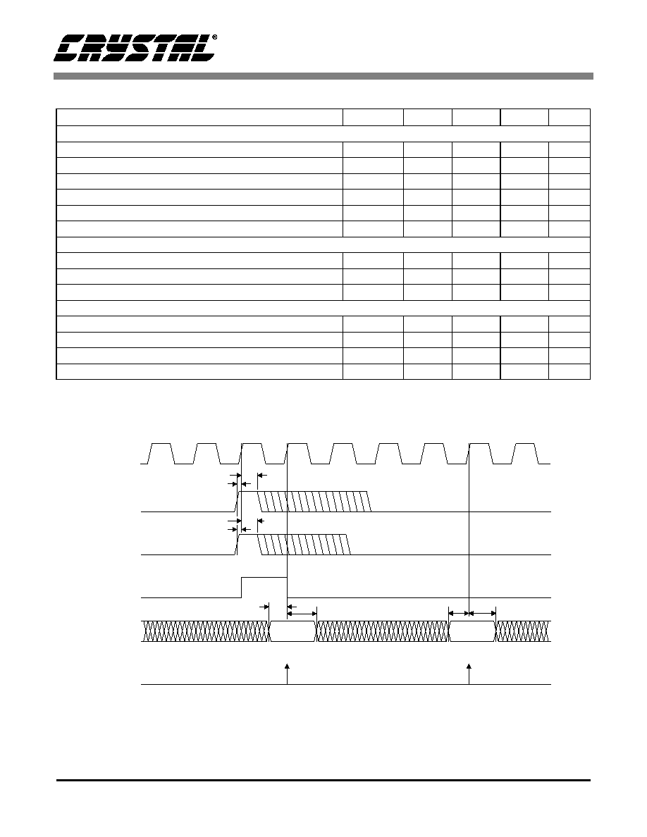
MSYNC Delay from MCLK rising
(Note 26)
t
msd
-
90
-
ns
t
mss
CLKIN
SYNC
LSYNC*
MCLK
MSYNC
MDATA
MFLG
* Internal timing signal generated in the CS5322
FILTER
SAMPLES
DATA
t
msd
t
msd
t
msh
t
msh
VALID DATA
VALID DATA
t
sh
t
ss
Figure 17. CS5320/21/CS5322 Interface Timing

CS5320/21/22
DS454PP1
15
CS5322 DIGITAL CHARACTERISTICS
(T
A
= (See Note 1); VD+ = 5.0V ± 5%; GND = 0V;
measurements performed under static conditions)
Notes: 27. Device is intended to be driven with CMOS logic levels.
28. Device is intended to be interfaced to CMOS logic. Resistive loads are not recommended on these pins.
CS5322 RECOMMENDED OPERATION CONDITIONS
(Voltages with respect to GND = 0V)
Notes: 29. The maximum voltage differential between the Positive Supply of the CS5320/21 and the Positive
Digital Supply of the CS5322 must be less than 0.25V.
CS5322 ABSOLUTE MAXIMUM RATINGS *
(Voltages with respect to GND = 0V)
Notes: 30. Transient currents of up to 100 mA will not cause SCR latch up.
*WARNING: Operation beyond these limits may result in permanent damage to the device. Normal operation is
not guaranteed at these extremes.
Parameter
Symbol
Min
Typ
Max
Units
High-Level Input Drive Voltage
V
IH
(VD+)-0.3
-
-
V
Low-Level Input Drive Voltage
V
IL
-
-
0.3
V
High-Level Input Threshold
(Note 27)
(VD+)-1.0
-
-
V
Low-Level Input Threshold
(Note 27)
-
-
1.0
V
High-Level Output Voltage IOUT = -40
µ
A
(Note 28)
V
OH
(VD+)-0.6
-
-
V
Low-Level Output Voltage IOUT = +1.6 mA
(Note 28)
V
OL
-
-
0.4
V
Input Leakage Current
All pins except MFLG, SOD
I
LKG
-
-
±10
µA
Three-State Leakage Current
I
OZ
-
-
±10
µA
Digital Input Capacitance
C
IN
-
9
-
pF
Digital Output Capacitance
C
OUT
-
9
-
pF
Parameter
Symbol
Min
Typ
Max
Units
DC Supply:
(Note 29)
Positive
Negative
VD+
VD-
4.75
-4.75
5.0
-5.0
5.25
-5.25
V
V
Ambient Operating Temperature
-KL
-BL
T
A
T
A
0
-40
-
-
+70
+85
°C
°C
Parameter
Symbol
Min
Typ
Max
Units
DC Supply:
(Note 29)
Positive
Negative
VD+
VD-
-0.3
0.3
-
-
(VD+)+0.3
-6.0
V
V
Input Current, Any Pin Except Supplies
(Note 30)
I
in
-
-
±10
mA
Digital Input Voltage
VIND
-0.3
-
(VD+)+0.3
V
Storage Temperature
T
stg
-65
-
150
°C
CS5320/21/22
16
DS454PP1
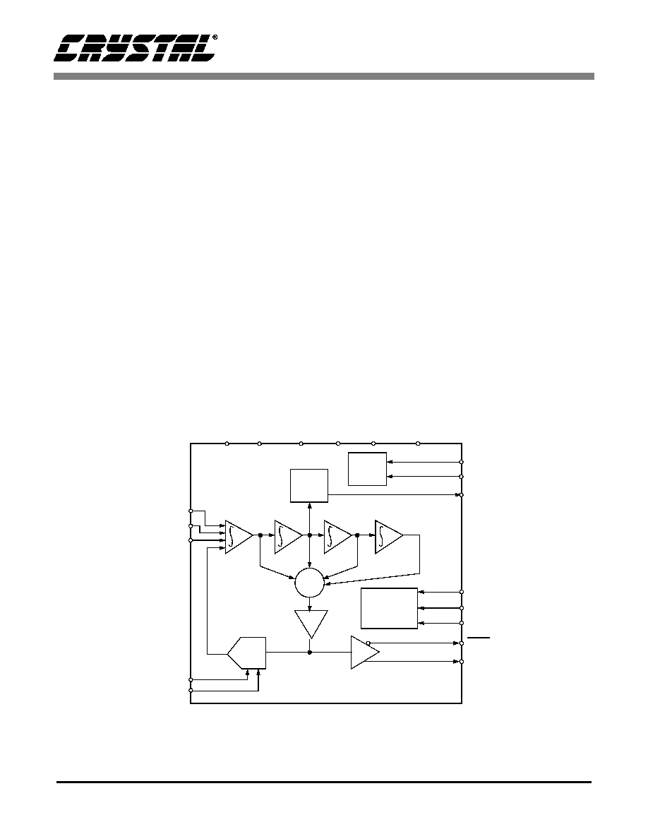
2. GENERAL DESCRIPTION
The CS5320 and CS5321 are fourth-order CMOS
monolithic analog modulators designed specifical-
ly for very high resolution measurement of signals
between dc and 1500 Hz. Configuring the CS5320
or CS5321 with the CS5322 FIR filter results in a
high resolution A/D converter system that performs
sampling and A/D conversion with dynamic range
exceeding 120 dB .
The CS5320 and CS5321 use a fourth-order over-
sampling architecture to achieve high resolution
A/D conversion. The modulator consists of a 1-bit
A/D converter embedded in a negative feedback
loop. The modulator provides an oversampled seri-
al bit stream at 256 kbits per second (HBR=1) and
128 kbits per second (HBR=0) operating with a
clock rate of 1.024 MHz. Figure 18 illustrates the
CS5320/CS5321 Block Diagram.
The CS5322 is a monolithic digital Finite Impulse
Response (FIR) filter with programmable decima-
tion. The CS5322 and CS5320/CS5321 are intend-
ed to be used together to form a unique high
dynamic range ADC chipset. The CS5322 provides
the digital anti-alias filter for the CS5320/CS5321
modulator output. The CS5322 consists of: a multi-
stage FIR filter, four registers (status, data, offset,
and configuration), a flexible serial input and out-
put port, and a 2-channel input data multiplexer
that selects data from the CS5320/CS5321 (MDA-
TA) or user test data (TDATA). The CS5322 deci-
mates (64x to 4096x) the output to any of seven
selectable up-date periods: 16, 8, 4, 2, 1, 0.5 and
0.25 milliseconds. Data is output from the digital
filter in a 24-bit serial format. Figure 19 illustrates
the CS5322 Block Diagram.
Figure 18. CS5320/21 Block Diagram
AINR
V
dd1
Osc.
Detect
AIN+
AIN-
VREF+
VREF-
D/A
A/D
Digital
Control
MDATA
MDATA
Clock
Generation
MSYNC
MCLK
HBR
MFLG
OFST
LPWR
V
ss1
AGND
V
dd2
V
ss2
DGND

CS5320/21/22
DS454PP1
17
SOD
SID
TDATA
MDATA
CSEL
PWDN
ORCAL
USEOR
DECC
DECB
DECA
SCLK
CLKIN
RESET
SYNC
MFLG
DRDY
MSYNC
MCLK
H/S
CS
R/W
ERROR
RSEL
CONFIG REG
CONFIG MUX
STATUS REG
BIT SELECT
MUX
BIT SELECT
DATA REG
FIR2
FIR3
FIR1
DATA MUX
CONTROL
Figure 19. CS5322 Block Diagram

CS5320/21/22
18
DS454PP1
2.1 Analog Input
The CS5320 and CS5321 modulators use a
switched capacitor architecture for its signal and
voltage reference inputs. The signal input uses three
pins; AINR, AIN+, and AIN-. The AIN- pin acts as
the return pin for the AINR and AIN+ pins. The
AINR pin is a switched capacitor "rough charge" in-
put for the AIN+ pin. The input impedance for the
rough charge pin (AINR) is 1/fC where f is two
times the modulator sampling clock rate and C is
the internal sampling capacitor (about 40 pF). Us-
ing a 1.024 MHz master clock (HBR = 1) yields an
input impedance of about 1/(512 kHz)X(40 pF) or
about 50 k
. Internal to the chip the rough charge
input pre-charges the sampling capacitor used on
the AIN+ input, therefore the effective input imped-
ance on the AIN+ pin is orders of magnitude above
the impedance seen on the AINR pin.
The analog input structure inside the VREF+ pin is
very similar to the AINR pin but includes addition-
al circuitry whose operating current can change
over temperature and from device to device. There-
fore, if gain accuracy is important, the VREF+ pin
should be driven from a low source impedance.
The current demand of the VREF+ pin will produce
a voltage drop of approximately 45 mV across the
200
source resistor of Figure 20 and Figure 21
Option A with MCLK = 1.024 MHz, HBR = 1, and
temperature = 25
°
C.
When the CS5320/21 modulator is operated with a
4.5 V reference it will accept a 9 V p-p input signal,
but modulator loop stability can be adversely af-
fected by high frequency out-of-band signals.
Therefore, input signals must be band-limited by an
input filter. The -3 dB corner of the input filter must
be equal to the modulator sampling clock divided
by 64. The modulator sampling clock is MCLK/4
when HBR = 1 or MCLK/8 when HBR = 0. With
MCLK = 1.024 MHz, HBR = 1, the modulator
sampling clock is 256 kHz which requires an input
filter with a -3 dB corner of 4 kHz. The bandlimit-
ing may be accomplished in an amplifier stage
ahead of the CS5320/21 modulator or with the RC
input filter at the AIN+ and AINR input pins. The
RC filter at the AIN+ and AINR pins is recom-
mended to reduce the "charge kick" that the driving
amplifier sees as the switched capacitor sampling is
performed.
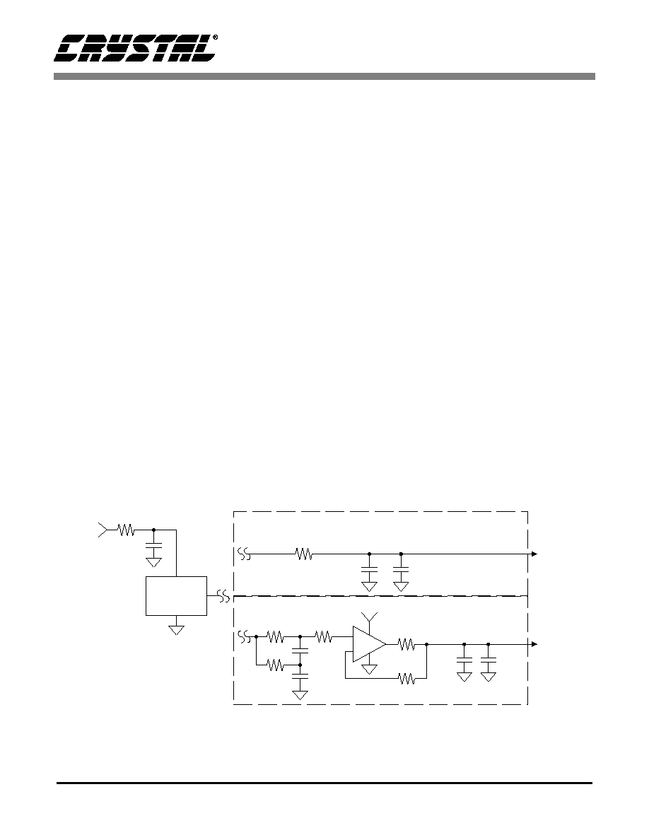
Figure 20 illustrates the CS5320/21 and CS5322
system connections. The input components on
AINR and AIN+ should be identical values for op-
timum performance. In choosing the components
the capacitor should be a minimum of 0.1
µ
F (C0G
dielectric ceramic preferred). For minimum board
space, the RC components on the AINR input can
be removed, but this will force the driving amplifi-
er to source the full dynamic charging current of
the AINR input. This can increase distortion in the
driving amplifier and reduce system performance.
In choosing the RC filter components, increasing C
and minimizing R is preferred. Increasing C reduc-
es the instantaneous voltage change on the pin, but
may require paralleling capacitors to maintain
smaller size (the recommended 0.1
µ
F C0G ceram-
ic capacitor is larger than other similar-valued ca-
pacitors with different dielectrics). Larger resistor
values will increase the voltage drop across the re-
sistor as the recharging current charges the
switched capacitor input.
2.2 The OFST Pin
The CS5320/21 modulator can produce "idle
tones" which occur in the passband when the input
signal is steady state dc signal within about
±
50 mV of bipolar zero. In the CS5320/21 these
tones are about 135 dB down from full scale. The
user can force these idle tones "out-of-band" by
adding 100 mV of dc offset to the signal at the AIN
input. Alternately, if the user circuitry has a low
offset voltage such that the input signal is within
±
50 mV of bipolar zero when no AC signal is
present, the OFST pin on the CS5320/21 can be ac-
tivated. When OFST = 1, +100 mV of input re-

CS5320/21/22
DS454PP1
19
ferred offset will be added internal to the
CS5320/21 and guarantee that any idle tones
present will lie out-of-band. The user should be
certain that when OFST is active (OFST =1) that
the offset voltage generated by the user circuitry
does not negate the offset added by the OFST pin.
2.3 Input Range and Overrange Conditions
The analog input is applied to the AIN+ and AINR
pins with the AIN- pin connected to GND. The in-
put is fully differential but for proper operation the
AIN- pin must remain at GND potential.
The analog input span is defined by the voltage ap-
plied between the VREF+ and VREF- input pins.
See the Voltage Reference section of this data sheet
for voltage reference requirements.
The modulator is a fourth order delta-sigma and is
therefore conditionally stable. The modulator may
go into an oscillatory condition if the analog input
is overranged. Input signals which exceed either
plus or minus full scale by more than 5 % can intro-
duce instability in the modulator. If an unstable
condition is detected, the modulator will be re-
duced to a first order system until loop stability is
achieved. If this occurs the MFLG pin will transi-
tion from a low to a high will result in an error bit
being set in the CS5322. The input signal must be
reduced to within the full scale range of the con-
verter for at least 32 MCLK cycles for the modula-
tor to recover from this error condition.
TDATA
VD+
DGND
+5 V
Digital
Supply
0.01
µ
F
SID
SOD
SCLK
CS
R/W
DRDY
RSEL
ERROR
CSEL
PWDN
USEOR
ORCAL
DECA
DECB
DECC
CLKIN
SYNC
Serial
Data
Interface
Unused logic
inputs must be
connected to
DGND or VD+
CS5322
Control
Hardware
VD+
DGND
+5 V
Digital
Supply
0.01
µ
F
H/S
RESET
3
2
11
21
20
25
24
26
1
28
22
27
23
12
13
14
15
19
18
17
16
4
9
8
GND1
VREF+
V
dd2
V
ss2
V
dd1
0.1
µ
F
0.1
µ
F
-5V
Analog
Supply
+5V
Analog
Supply
CS5320/21
0.1
µ
F
Test
Data
+
10
µ
F
+
10
µ
F
2
22
21
5
1
GND2
V
ss1
0.1
µ
F
3
4
GND9
GND10
GND8
+4.5V
VREF
0.1
µ
F
68
µ
F
+
TANT.
19
16
15
VREF-
6
AIN+
0.1
µ
F
9
Signal
Source
COG
AIN-
8
AINR
10
GND5
12
GND6
13
GND3
7
GND4
11
14
GND7
402
MSYNC
5
MSYNC
25
MFLG
6
MFLG
24
MCLK
7
MCLK
20
MDATA
10
MDATA
18
GND11
23
OFST
28
LPWR
27
HBR
26
Control
Logic
Clock
Source
17
MDATA
200
0.1
µ
F
COG
402
Figure 20. System Connection Diagram
CS5320/21/22
20
DS454PP1
2.4 Voltage Reference
The CS5320/21 is designed to operate with a volt-
age reference in the range of 4.0 to 4.5 volts. The
voltage reference is applied to the VREF+ pin with
the VREF- pin connected to the GND. A 4.5 V ref-
erence will result in the best S/N performance but
most 4.5 V references require a power supply volt-
age greater than 5.0 V for operation. A 4.0 V refer-
ence can be used for those applications which must
operate from only 5.0 V supplies, but will yield a
S/N slightly lower (1-2 dB) than when using a 4.5
V reference. The voltage reference should be de-
signed to yield less than 2
µ
V rms of noise in band
at the VREF+ pin of the CS5320/21. The CS5322
filter selection will determine the bandwidth over
which the voltage reference noise will affect the
CS5320/21/22 dynamic range.
For a 4.5 V reference, the LT1019-4.5 voltage ref-
erence yields low enough noise if the output is fil-
tered with a low pass RC filter as shown in Figure
21 Option A. The filter in Figure 21 Option A is ac-
ceptable for most spectral measurement applica-
tions, but a buffered version with lower source
impedance (Figure 21 Option B) may be preferred
for dc-measurement applications. Due to its dy-
namic (switched-capacitor) input the input imped-
ance of the +VREF pin of the CS5320/21 will
change any time MCLK or HBR is changed. There-
fore the current required from the voltage reference
will change any time MCLK or HBR is changed.
This can affect gain accuracy due to the high source
impedance of the filter resistor in Figure 20 and
Figure 21 Option A. If gain error is to be mini-
mized, especially when MCLK or HBR is changed,
the voltage reference should have lower output im-
pedance. The buffer of Figure 21 Option B offers
lower output impedance and will exhibit better sys-
tem gain stability.
2.5 Clock Source
For proper operation, the CS5320/21 must be pro-
vided with a CMOS-compatible clock on the
MCLK pin. The MCLK for the CS5320/21 is usu-
ally provided by the CS5322 filter. MCLK is usu-
ally 1.024 MHz to set the seven selectable output
word rates from the CS5322. The MCLK frequency
can be as low as 250 kHz and as high as 1.2 MHz.
The choice of clock frequency can affect perfor-
mance; see the Performance section of the data
0.1
µ
F
+9 to
15V
10
LT1019-4.5
200
+
-
49.9
1k
100
1k
10k
100
µ
F
AL
100
µ
F
AL
+9 to 15V
0.1
µ
F
+
+
68
µ
F
Tant
+
0.1
µ
F
68
µ
F
+
To VREF+
To VREF+
LT1007
Option A
Option B
Figure 21. 4.5 Voltage Reference with two filter options
CS5320/21/22
DS454PP1
21
sheet. The clock must have less than 300 ps jitter to
maintain data sheet performance from the device.
The CS5320/21 is equipped with loss of clock de-
tection circuitry which will cause the CS5320/21 to
enter a powered-down state if the MCLK is re-
moved or reduced to a very low frequency. The
HBR pin on the CS5320/21 modifies the sampling
clock rate of the modulator. When HBR = 1, the
modulator sampling clock will be at MCLK/4; with
HBR = 0 the modulator sampling clock will be at
MCLK/8. The chip set will exhibit about 3 dB less
S/N performance when the HBR pin is changed
from a logic "1" to a logic "0" for the same output
word rate from the CS5322.
2.6 Low Power Mode
The CS5320/21 includes a low power operating
mode (LPWR =1). When operated with LPWR = 1,
the CS5320/21 modulator sampling clock must be
restricted to rates of 128 kHz or less. Operating in
low power mode with modulator sample rates
greater than 128 kHz will greatly degrade perfor-
mance.
2.7 Digital Interface and Data Format
The MCLK signal (normally 1.024 MHz) is divid-
ed by four, or by eight inside the CS5320/21 to gen-
erate the modulator oversampling clock. The HBR
pin determines whether the clock divider inside the
CS5320/21 divides by four (HBR =1) or by eight
(HBR = 0). The modulator outputs a ones density
bit stream from its MDATA and MDATA pins pro-
portional to the analog input signal, but at a bit rate
determined by the modulator over sampling clock.
For proper synchronization of the bitstream, the
CS5320/21 must be furnished with an MSYNC sig-
nal prior to data conversion. The MSYNC signal,
generated by the CS5322, resets the MCLK
counter-divider in the CS5320/21 to the correct
phase so that the bitstream can be properly sampled
by the CS5322 digital filter.
When operated with the CS5322 digital filter the
output codes from the CS5320/21/22 will range
from approximately decimal -5,242,880 to
+5,242,879 for an input to the CS5320/21 of
±
4.5
V. Table 1 illustrates the output coding for various
input signal amplitudes. Note that with a signal in-
put defined as a full scale signal (4.5 V with
VREF+ = 4.5 V) the CS5320/22 and CS5321/22
chipsets does not output a full scale digital code of
8,388,607 but is scaled to a lower value to allow
some overrange capability. Input signals can ex-
ceed the defined full scale by up to 5% and still be
converted properly.
Modulator Input
Signal
CS5322 Filter
Output Code
HEX
Decimal
> (+VREF + 5%)
Error Flag Possible
(+VREF + 5%)
53FFFF(H)
+5505023
+VREF
4FFFFF(H)
+5242879
0V
000000(H)
0
-VREF
B00000(H)
-5242880
- (+VREF +5%)
AC0000(H)
-5505024
> - (+VREF +5%)
Error Flag Possible
Table 1. Output Coding for the CS5320/21 and
CS5322 Combination
CS5320/21/22
22
DS454PP1
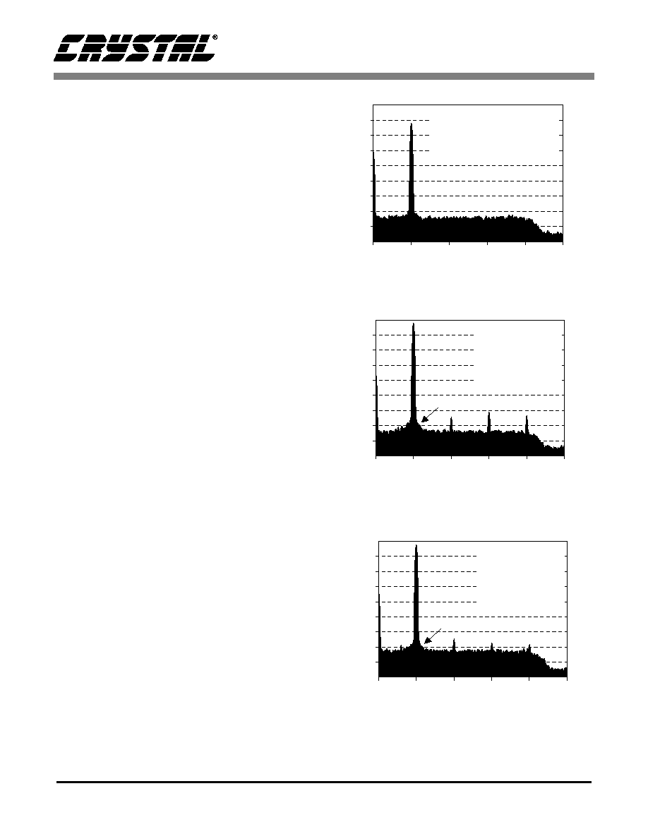
2.8 Performance
Figure 22, 23 and 24 illustrate the spectral perfor-
mance of the CS5321/22 and CS5320/22 chipsets
when operating from a 1.024 MHz master clock.
Ten 1024 point FFTs were averaged to produce the
plots.
Figure 22 illustrates the chip set with a 100 Hz,
-20 dB input signal. The sample rate was set at 1
kHz. Dynamic range is 122 dB.
The dynamic range calculated by the test soft-ware
is reduced somewhat in Figures 23 and 24 because
of jitter in the signal test oscillator. Jitter in the
100 Hz signal source is interpreted by the signal
processing software to be increased noise.
The choice of master clock frequency will affect
performance. The CS5320/21 will exhibit the best
Signal/ Distortion performance with slower modu-
lator sampling clock rates as slower sample rates
allow more time for amplifier settling.
For lowest offset drift, the CS5320/21 should be
operated with MCLK = 1.024 MHz and HBR = 1.
Slower modulator sampling clock rates will exhibit
more offset drift. Changing MCLK to 512 kHz
(HBR = 1) or changing HBR to zero (MCLK =
1.024 MHz) will cause the drift rate to double. Off-
set drift is not linear over temperature so it is diffi-
cult to specify an exact drift rate. Offset drift
characteristics vary from part to part and will vary
as the power supply voltages vary. Therefore, if the
CS5320/21 is to be used in precision dc measure-
ment applications where offset drift is to be mini-
mized, the power supplies should be well
regulated. The CS5320/21 will exhibit about
6 ppm/°C of offset drift with MCLK = 1 and HBR
= 1.
Gain drift of the CS5320/21 itself is about
5 ppm/°C and is not affected by either modulator
sample rate or by power supply variation.
Figure 22. 1024 Point FFT Plot with -20 dB Input, 100
Hz Input, ten averages
Dynamic Range = 122.0 dB
HBR = 1
OFST = 0
LPWR = 0
0
500
0
-20
-40
-60
-80
-100
-120
-140
-160
-180
Figure 23. 1024 Point FFT Plot with Full Scale Input,
100 Hz Input, HBR = 1, ten averages
S/D = 116.0 dB
S/N = 118.4 dB
S/N+D = 114.2 dB
HBR = 1
OFST = 0
LPWR = 0
0
500
0
-20
-40
-60
-80
-100
-120
-140
-160
-180
see text
Figure 24. 1024 Point FFT Plot with Full Scale Input,
100 Hz Input, HBR = 0, ten averages
0
500
0
-20
-40
-60
-80
-100
-120
-140
-160
-180
S/D = 122.7 dB
S/N = 117.1 dB
S/N+D = 116.4 dB
HBR = 0
OFST = 0
LPWR = 0
see text

CS5320/21/22
DS454PP1
23
2.9 Power Supply Considerations
The system connection diagram, Figure 20, illus-
trates the recommended power supply arrange-
ments. There are two positive power supply pins
for the CS5320/21 and two negative power supply
pins. Power must be supplied to all four pins and
each of the supply pins should be de-coupled with
a 0.1
µ
F capacitor to the nearest ground pin on the
device.
When used with the CS5322 digital filter, the max-
imum voltage differential between the positive sup-
plies of the CS5320/21 and the positive digital
supply of the CS5322 must be less than 0.25 V. Op-
eration beyond this constraint may result in loss of
analog performance in the CS5320/22 and
CS5321/22 system performance.
Many seismic or portable data acquisition systems
are battery powered and utilize dc-dc converters to
generate the necessary supply voltages for the sys-
tem. To minimize the effects of power supply inter-
ference, it is desirable to operate the dc-dc
converter at a frequency which is rejected by the
digital filter, or locked to the modulator sample
clock rate.
A synchronous dc-dc converter, whose operating
frequency is derived from the 1.024 MHz clock
used to drive the CS5322, will minimize the poten-
tial for "beat frequencies" appearing in the
pass-
band between dc and the corner frequency of the
digital filter.
2.10 Power Supply Rejection Ratio
The PSRR of the CS5320/21 is frequency depen-
dent. The CS5322 digital filter attenuation will aid
in rejection of power supply noise for frequencies
above the corner frequency setting of the CS5322.
For frequencies between dc and the corner frequen-
cy of the digital filter, the PSRR is nearly constant
at about 60 dB.
2.11 RESET Operation
The RESET pin puts the CS5322 into a known ini-
tialized state. RESET is recognized on the next
CLKIN rising edge after the RESET pin has been
brought high (RESET=1). All internal logic is ini-
tialized when RESET is active.
Normal device operation begins on the second
CLKIN rising edge after RESET is brought low.
The CS5322 will remain in an idle state, not per-
forming convolutions, until triggered by a SYNC
event.
A RESET operation clears memory, sets the data
output register, offset register, and status flags to all
zeroes, and sets the configuration register to the
state of the corresponding hardware pins (PWDN,
ORCAL, DECC, DECB, DECA, USEOR, and
CSEL). The reset state is entered on power on, in-
dependent of the RESET pin. If RESET is low, the
first CLKIN will exit the power on reset state.
2.12 Power-down Operation
The PWDN pin puts the CS5322 into the power-
down state. The power-down state is entered on the
first CLKIN rising edge after the PWDN pin is
brought high. While in the power-down state, the
MCLK and MSYNC signals to the CS5320/21 an-
alog modulator are held low. The loss of the MCLK
signal to the modulator causes it to power-down.
The signals on the MDATA and MFLG pins are ig-
nored. The serial interface of the CS5322 remains
active allowing read and write operations. Informa-
tion in the data register, offset register, configura-
tion register, and convolution data memory are
maintained during power-down. The internal con-
troller requires 64 clock cycles after PWDN is as-
serted before CLKIN stops.
The CS5322 exits the power-down state on the first
CLKIN rising edge after the PWDN pin is brought
low. The CS5322 then enters an idle state until trig-
gered by a SYNC event.

CS5320/21/22
24
DS454PP1
To avoid possible high current states while in the
power down state, the following conditions apply:
1) CLKIN must be active for at least 64 clock cy-
cles after PWDN entry.
2) CSEL and TDATA must not both be asserted
high.
2.13 SYNC Operation
The SYNC pin is used to start convolutions and
synchronize the CS5322 and CS5320/21 to an ex-
ternal sampling source or timing reference. The
SYNC event is recognized on the first CLKIN ris-
ing edge after the SYNC pin goes high. SYNC may
remain high indefinitely. Only the sequence of
SYNC rising followed by CLKIN rising generates
a SYNC event.
The SYNC event aligns the output sample and
causes the filter to begin convolutions. The first
SYNC event causes an immediate DRDY provided
DRDY is low. Subsequent data ready events will
occur at a rate determined by the decimation rate
inputs DECC, DECB, and DECA. Multiple SYNC
events can be applied with no effect on operation if
they are perfectly timed according to the decima-
tion rate. Any SYNC event not in step with the dec-
imation rate will cause a realignment and loss of
data.
2.14 Serial Read Operation
Serial read is used to obtain status or conversion
data. The CS, R/W, SCLK, RSEL, and SOD pins
control the read operation. The serial read opera-
tion is activated when CS goes low (CS=0) with the
R/W pin high (R/W=1). The RSEL pin selects be-
tween conversion data (data register) or status in-
formation (status register). The selected serial bit
stream is output on the SOD (Serial Output Data)
pin.
On read select, SCLK can either be high or low, the
first bit appears on the SOD pin and should be
latched on the falling edge of SCLK. After the first
SCLK falling edge, each SCLK rising edge shifts
out a new bit. Status reads are 16 bits, and data
reads are 24 bits. Both streams are supplied as MSB
first, LSB last.
In the event more SCLK pulses are supplied than
necessary to clock out the requested information,
trailing zeroes will be output for data reads and
trailing LSB's for status reads. If the read operation
is terminated before all the bits are read, the inter-
nal bit pointer is reset to the MSB so that a re-read
will give the same data as the first read, with one
exception. The status error flags are cleared on read
and will not be available on a re-read.
The status error flags must be read before entering
the power-down state. If an error has occurred be-
fore entering powerdown and the status bit (ER-
ROR) has not been read, the status bits (ER-ROR,
OVERWRITE, MFLG, ACC1 and ACC2) may not
be cleared on status reads. Upon exiting the power-
down state and entering normal operation, the user
may be flagged that an error is still present.
The SOD pin floats when read operation is deacti-
vated (R/W=1, CS=1). This enables the SID and
SOD pins to be tied together to form a bi-direction-
al serial data bus. There is an internal nominal
100 k
pull-up resistor on the SOD pin.
2.15 Serial Write Operation
Serial write is used to write data to the configura-
tion register. The CS, R/W, SCLK and SID pins
control the serial write operation. The serial write
operation is activated when CS goes low (CS=0)
with R/W pin low (R/W=0).
Serial input data on the SID pin is sampled on the
falling edge of SCLK. The input bits are stored in a
temporary buffer until either the write operation is
terminated or 8 bits have been received. The data is
then parallel loaded into the configuration register.
If fewer than 8 bits are input before the write termi-
nation, the other bits may be indeterminate.
CS5320/21/22
DS454PP1
25
Note that a write will occur when CS = 0 and R/W
= 0 even if SCLK is not toggled. Failure to clock in
data with the appropriate number of SCLKs can
leave the configuration register in an indeterminate
condition.
The serial bit stream is received MSB first, LSB
last. The order of the input control data is PWDN
first, followed by ORCAL, USEOR, CSEL, Re-
served, DECC, DECB, and DECA. The configura-
tion data bits are defined in Table 2. The
configuration data controls device operation only
when in the software mode, i.e., the H/S pin is low
(H/S = 0). The Reserved configuration data bit
must always be written low.
2.16 Offset Calibration Operation
The offset calibration routine computes the offset
produced by the CS5320/21 modulator and stores
this value in the offset register. The USEOR pin or
bit determines if the offset register data is to be
used to correct output words.
After power is applied to the chip set the CS5322
must be RESET. To begin an offset calibration, the
CS5320/21 analog input must represent the offset
value. Then in software mode (H/S = 0) the OR-
CAL bit must be toggled from a low to a high. In
hardware mode the ORCAL pin must be toggled
low for at least one CLKIN cycle, then taken high
(except when ORCAL = 1 and the CS5322 is RE-
SET as this toggles the ORCAL internally). After
ORCAL has been toggled, the SYNC signal must
be applied to the CS5322. The filter settles on the
input value in 56 output words. The output word
rate is determined by the state of the decimation
rate control pins, DECC, DECB, and DECA. On
the 57th output word, the CS5322 issues the OR-
CALD status flag, outputs the offset data sample,
and internally loads the offset register. During cal-
ibration, the offset register value is not used.
If USEOR is high (USEOR=1), subsequent sam-
ples will have the offset subtracted from the output.
The state of USEOR must remain high for the com-
plete duration of the convolution cycle. If USEOR
is low (USEOR=0), the output word is not correct-
ed, but the offset register retains its value for later
use. The results of the last calibration will be held
in the offset register until the end of a new calibra-
tion, or until the CS5322 is reset using the RESET
pin. USEOR does not alter the offset register value,
only its usage.
To restart a calibration, ORCAL and SYNC must
be taken low for at least one CLKIN cycle. OR-
CAL must then be taken high. The calibration will
restart on the next SYNC event. If the ORCAL pin
remains in a high state, only a single calibration
will start on the first SYNC signal.
Input Bit #
Equivalent Hardware
Function
Description
1 (MSB)
PWDN
Standby mode
2
ORCAL
Self-offset calibration
3
USEOR
Use Offset Register
4
CSEL
Channel Select
5
Reserved
Factory use only
6
DECC
Filter BW selection
7
DECB
Filter BW selection
8 (LSB)
DECA
Filter BW selection
Table 2. Configuration Data Bits
CS5320/21/22
26
DS454PP1
2.17 Status Bits
The Status Register is a 16-bit register which al-
lows the user to read the flags and configuration
settings of the CS5322. Table 3 documents the data
bits of the Status Register.
The ERROR flag, ERROR, is the OR'ed result of
OVERWRITE, MFLG, ACC1, and ACC2. The
ERROR bit is active high whenever any of the four
error bits are set due to a fault condition. The ER-
ROR output has a nominal 100 K
internal pull-up
resistor.
The OVERWRITE bit is set when new conversion
data is ready to be loaded into the data register, but
the previous data was not completely read out. This
can occur on either of two conditions: a read oper-
ation is in progress or a read operation was started,
then aborted, and not completed. These two condi-
tions are data read attempts. The attempt is identi-
fied by the first SCLK low edge (MSB read) of a
data register read. If a data register read is not at-
tempted, the CS5322 assumes that data is not want-
ed and does not assert OVERWRITE, and the old
data is over-written by the new data. On an OVER-
WRITE condition, the old partially read data is pre-
served, and the new data word is lost.
Status reads have no effect on OVERWRITE assert
operations. The OVERWRITE bit is cleared on a
status register read or RESET.
The MFLG error bit reflects the CS5320/21 MFLG
signal. Any high level on the CS5322 MFLG pin
will set the MFLG status bit. The bit is cleared on a
status register read or RESET operation, only if the
MFLG pin on the CS5322 has returned low. A in-
ternal nominal 100 K
pulldown resistor is on the
MFLG pin.
The accumulator error bits, ACC1 and ACC2, indi-
cate that an underflow or overflow has occurred in
the FIR1 filter for ACC1, or the FIR2 and FIR3 fil-
ters for ACC2. Both errors are cleared on a status
read, provided the error conditions are no longer
Output Bit #
Function
Description
1 (MSB)
Error
Detects one of the errors below
2
OVERWRITE Error
Overwrite Error
3
MFLG Error
Modulator Flag Error
4
ACC1 Error
Accumulator 1 Error
5
ACC2 Error
Accumulator Error
6
DRDY
Data Ready
7
1SYNC
First sample after SYNC
8
ORCALD
Offset calibration done
9
PWDN
Standby mode
10
ORCAL
Self-offset Calibration
11
USEOR
Use Offset Register
12
CSEL
Channel Select
13
Reserved
Factory use only
14
DECC
Bandwidth Selection Status
15
DECB
Bandwidth Selection Status
16
DECA
Bandwidth Selection Status
Table 3. Status Data (from the SOD Pin)
CS5320/21/22
DS454PP1
27
present. In normal operation the ACC1 error will
only occur when the input data stream to FIR1 is all
1's for more than 32 bits. The ACC2 error cannot
occur in normal operation.
The DRDY bit reflects the state of the DRDY pin.
DRDY rising edge indicates that a new data word
has been loaded into the data register and is avail-
able for reading. DRDY will fall after the SCLK
falling edge that reads the data register LSB. If no-
data read attempt is made, DRDY will pulse low
for 1/2 CLKIN cycle, providing a positive edge on
the new data availability. In the OVERWRITE
case, DRDY remains high because new data is not
loaded at the normal end of conversion time.
The 1SYNC status bit provides an indication of the
filter group delay. It goes high on the second output
sample after SYNC and is valid for only that sam-
ple. For repetitive SYNC operations, SYNC must
run at one fourth the output word rate or slower to
avoid interfering with the 1SYNC operation. With
these slower repetitive SYNC's or non-periodic
SYNC's separated by at least three output words,
1SYNC will occur on the second output sample af-
ter SYNC.
ORCALD indicates that calibration of the offset
register is complete and the offset sample is avail-
able in the output register. This flag is high only
during that sample and is otherwise low.
The remaining five status bits (PWDN, ORCAL,
USEOR, CSEL, Reserved, DECC, DECB, and DE-
CA) provide configuration readback for the user.
These bits echo the control source for the CS5322
such that in the hardware mode (H/S=1), they fol-
low the corresponding input pins. In host mode
(H/S=0) they follow the corresponding configura-
tion bits.
A brief explanation of the eight bits are as follows:
PWDN - When high, indicates that the CS5322 is in
the power-down state.
ORCAL - When high, indicates a potential calibra-
tion start.
USEOR - When high, indicates the Offset Register is
used. During calibration, this bit will read zero indi-
cating the offset register is not being used during cal-
ibration.
CSEL- When high, TDATA is selected as the filter
source. When low, the MDATA output signal from
the CS5320/21 is selected as the input source to the
filter.
Reserved - Always read low.
DECC, DECB, and DECA - Indicate the decimation
rate of the filter and are defined in Table 4.
DECC
DECB
DECA
Output Word Rate (Hz)
Clocks Filter Output
0
0
0
62.5
16384
0
0
1
125
8192
0
1
0
250
4096
0
1
1
500
2048
1
0
0
1000
1024
1
0
1
2000
512
1
1
0
4000
256
1
1
1
Reserved
-
Table 4. Bandwidth Selection: Truth Table

CS5320/21/22
28
DS454PP1
2.18 Board Layout Considerations
All of the 0.1
µ
F filter capacitors on the power sup-
plies, AIN+, and AINR, should be placed very
close to the chip and connect to the nearest ground
pin on the device. The capacitors between VREF+
and VREF- should be located as close to the chip as
possible. The 0.l
µ
F capacitors on the AIN+ and
AINR pins should be placed with their leads on the
same axis, not side-by-side. If these capacitors are
placed side-by-side their electric fields can interact
and cause increased distortion. The chip should be
surrounded with a ground plane. Trace fill should
be used around the analog input components.
See AN18: Layout and Design Rules for Data Con-
verters for further information.
CS5320/21/22
DS454PP1
29
3. CS5320/21 PIN DESCRIPTIONS
Power Supplies
V
dd1
Positive Power One, PIN 2
Positive supply voltage. Nominally +5 Volts.
V
dd2
Positive Power Two, PIN 22
Positive supply voltage. Nominally +5 Volts.
V
ss1
Negative Power One, PIN 3
Negative supply voltage. Nominally -5 Volts.
V
ss2
Negative Power Two, PIN 21
Negative supply voltage. Nominally -5 Volts.
GND1 through GND11 Ground, PINS 1, 4, 7, 11, 12, 13, 14, 15, 16, 19, 23.
Ground reference.
Analog Inputs
AIN+ - Positive Analog Input, PIN 9
Nominally
±
4.5V
AIN- - Negative Analog Input, PIN 8
This pin is tied to ground.

CS5320/21/22
30
DS454PP1
AINR - Analog Input Rough, PIN 10
Allows a non-linear current to bypass the main external anti-aliasing filter which if allowed to
happen, would cause harmonic distortion in the modulator. Please refer to the System
Connection Diagram and the Analog Input and Voltage Reference section of the data sheet for
recommended use of this pin.
VREF+ Positive Voltage Reference Input, PIN 5
This pin accepts an external +4.5 V voltage reference.
VREF- Negative Voltage Reference Input, PIN 6
This pin is tied to ground.
Digital Inputs
MCLK Clock Input, PIN 20
A CMOS-compatible clock input to this pin (nominally 1.024 MHz) provides the necessary
clock for operation of the modulator and data output portions of the A/D converter. MCLK is
normally supplied by the CS5322
MSYNC Modulator Sync, PIN 25
A transition from a low to high level on this input will re-initialize the CS5320/21. MSYNC
resets a divider-counter to align the MDATA output bit stream from the CS5320/21 with the
timing inside the CS5322.
OFST - Offset, PIN 28
When high, adds approximately 100 mV of input referred offset to guarantee that any zero
input limit cycles are out of band if present. When low, zero offset is added.
LPWR - Low Power Mode, PIN 27
The CS5320/21 power dissipation can be reduced from its nominal value of 55 mW to 30 mW
under the following conditions:
LPWR=1; MCLK = 512 kHz, HBR=1; or LPWR=1; MCLK = 1.024 MHz, HBR=0
HBR High Bit Rate, Pin 26
Selects either
1
/
4
MCLK (HBR=1) or
1
/
8
MCLK (HBR=0) for the modulator sampling clock.
Digital Outputs
MDATA Modulator Data Output, PIN 18
Data will be presented in a one-bit serial data stream at a bit rate of 256 kHz (HBR=1) or
128 kHz (HBR=0) with MCLK operating at 1.024 MHz.
MDATA Modulator Data Output, PIN 17
Inverse of the MDATA output.
MFLG Modulator Flag, PIN 24
A transition from a low to high level signals that the CS5320/21 modulator is unstable due to
an over-range on the analog input

CS5320/21/22
DS454PP1
31
4. CS5322 PIN DESCRIPTIONS
Power Supplies
VD+ Positive Digital Power, Pin 8, 21
Positive digital supply voltage. Nominally +5 volts.
DGND Digital Ground, Pin 9, 20
Digital ground reference.
Digital Outputs
MCLK Modulator Clock Output, Pin 7
A CMOS-compatible clock output (nominally 1.024 MHz) that provides the necessary clock for
operation of the modulator.
MSYNC Modulator Sync, Pin 5
The transition from a low to high level on this output will re-initialize the CS5320/21.
ERROR - Error Flag, Pin 23
This signal is the output of an open pull-up NOR gate with a nominal 100 k
pull-up resistor
to which the error status data (OVERWRITE error, MFLG error, ACC1 error and ACC2 error)
are inputs. When low, it notifies the host processor that an error condition exists. The ERROR
signal can be wire OR'd together with other filters' outputs. The value of the internal pull-up
resistor is 100 k
.
DRDY - Data Ready, Pin 22
When high, data is ready to be shifted out of the serial port data register.
TOP
VIEW
22
20
24
19
21
23
25
3
27
2
4
2 6
28
1
12
14
16
18
13
15
17
8
6
10
5
7
9
11
CHIP SELECT
CS
FRAME SYNC
SYNC
R/W
READ/WRITE
CLOCK INPUT
CLKIN
RSEL
REGISTER SELECT
RESET RESET
SCLK
SERIAL CLOCK
MODULATOR SYNC MSYNC
SID
SERIAL INPUT DATA
MODULATOR FLAG
MFLG
SOD
SERIAL OUTPUT DATA
MODULATOR CLOCK
MCLK
CS5322
ERROR ERROR FLAG
POSITIVE DIGITAL POWER
VD+
DRDY
DATA READY
DIGITAL GROUND
DGND
VD+
POSITIVE DIGITAL POWER
MODULATOR DATA MDATA
DGND
DIGITAL GROUND
TEST DATA TDATA
ORCAL OFFSET CALIBRATION
CHANNEL SELECT
CSEL
DECA
DECIMATION RATE CONTROL
HARDWARE/SOFTWARE MODE
H/S
DECIMATION RATE CONTROL
POWER DOWN PWDN
DECB
DECC
DECIMATION RATE CONTROL
USEOR USE OFFSET REGISTER

CS5320/21/22
32
DS454PP1
SOD - Serial Output Data, Pin 24
The output coding is 2's complement with the data bits presented MSB first, LSB last. Data
changes on the rising edge of SCLK. An internal nominal 100 k
pull-up resistor is included.
Digital Inputs
MDATA Modulator Data, Pin 10
Data will be presented in a one-bit serial data stream at a bit rate of 256 KHz; (CLKIN =
1.024 MHz).
TDATA - Test Data, Pin 11
Input for user test data.
MFLG Modulator Flag, Pin 6
A transition from a low to high level signals that the CS5320/21 modulator is unstable due to
an over-range on the analog input. A Status Bit will be set in the digital filter indicating an
error condition. An internal nominal 100 k
pull-down resistor included on the input pin.
RESET - Filter Reset, Pin 4
Performs a hard reset on the chip, all registers and accumulators are cleared. All signals to the
device are locked out except CLKIN. The error flags in the Status Register are set to zero and
the Data Register and Offset Register are set to zero. The configuration register is set to the
values of the corresponding input pins. SYNC must be applied to resume convolutions after
RESET deasserts.
CLKIN - Clock Input, Pin 3
A CMOS-Compatible clock input to this pin (nominally 1.024 MHz) provides the necessary
clock for operation the modulator and filter.
SYNC - Frame Sync, Pin 2
Conversion synchronization input. This signal synchronizes the start of the filter convolution.
More than one SYNC signal can occur with no effect on filter performance, providing the
SYNC signals are perfectly timed at intervals equal to the output sample period.
CSEL - Channel Select, Pin 12
When high, information on the TDATA pin is presented to the digital filter. A low causes data
on the MDATA input to be presented to the digital filter.
PWDN - Powerdown, Pin 14
Powers down the filter when taken high. Convolution cycles in the digital filter and the MCLK
signal are stopped. The registers maintain their data and the serial port remains active. SYNC
must be applied to resume convolutions after PWDN deasserts.
DECA - Decimation Rate Control, Pin 18
See Table 4.
DECB - Decimation Rate Control, Pin 17
See Table 4.

CS5320/21/22
DS454PP1
33
DECC - Decimation Rate Control, Pin 16
See Table 4.
H/S - Hardware/Software Mode Select, Pin 13
When high, the device pins control device operation; when low, the value entered by a prior
configuration write controls device operation.
CS - Chip Select, Pin 1
When high, all signal activity on the SID, R/W and SCLK pins is ignored. The DRDY and
ERROR signals indicate the status of the chip's internal operation.
R/W - Read/Write, Pin 28
Used in conjunction with CS such that when both signals are low, the filter inputs data from the
SID pin on the falling edge of SCLK. If CS is low and R/W is high, the filter outputs data on
the SOD pin on the rising edge of SCLK. R/W low floats the SOD pin allowing SID and SOD
to be tied together, forming a bidirectional serial data bus.
SCLK - Serial Clock, Pin 26
Clock signal generated by host processor to either input data on the SID input pin, or output
data on the SOD output pin. For write, data must be valid on the SID pin on the falling edge of
SCLK. Data changes on the SOD pin on the rising edge of SCLK.
SID - Serial Data Input, Pin 25
Data bits are presented MSB first, LSB last. Data is latched on the falling edge of SCLK.
RSEL - Register Select, Pin 27
Selects conversion data when high, or status data when low.
USEOR - Use Offset Register, Pin 15
Use offset register value to correct output words when high. Output words will not be offset
corrected when low.
ORCAL - Offset Register Calibrate, Pin 19
Initiates an offset calibration cycle when SYNC goes high after ORCAL has been toggled from
low to high. The offset value is output on the 57th word following SYNC. Subsequent words
will have their offset correction controlled by USEOR.

CS5320/21/22
34
DS454PP1
5. ORDERING INFORMATION
Kits
Analog Modulator
Digital Filter
Part Number
Part Number
Temperature
Package
Part Number
Temperature
Package
CK5320-KL1
CS5320-KL
0
o
to +70
o
C
28-pin PLCC
CS5322-KL
0
o
to +70
o
C
28-pin PLCC
CK5321-KL1
CS5321-BL
-55
o
to +85
o
C
28-pin PLCC
CS5322-KL
0
o
to +70
o
C
28-pin PLCC
CK5321-BL1
CS5321-BL
-55
o
to +85
o
C
28-pin PLCC
CS5322-BL
-40
o
to +85
o
C
28-pin PLCC
Table 5. Detailed Ordering Information

CS5320/21/22
DS454PP1
35
6. PARAMETER DEFINITIONS
Dynamic Range
The ratio of the full-scale (rms) signal to the broadband (rms) noise signal. Broadband noise is
measured with the input grounded within the bandwidth of 1 Hz to f
3
Hz (See "CS5322
FILTER CHARACTERISTICS" on page 8). Units in dB.
Signal-to-Distortion
The ratio of the full-scale (rms) signal to the rms sum of all harmonics up to f
3
Hz.
Units in dB.
Intermodulation Distortion
The ratio of the rms sum of the two test frequencies (30 and 50 Hz) which are each 6 dB down
from full-scale to the rms sum of all intermodulation components within the bandwidth of dc to
f
3
Hz. Units in dB.
Full Scale Error
The ratio of the difference between the value of the voltage reference and analog input voltage
to the full scale span (two times the voltage reference value). This ratio is calculated after the
effects of offset and the external bias components are removed and the analog input voltage is
adjusted. Measurement of this parameter uses the circuitry illustrated in the System Connection
Diagram. Units in %.
Full Scale Drift
The change in the Full Scale value with temperature. Units in %/
°
C.
Offset
The difference between the analog ground and the analog voltage necessary to yield an output
code from the CS5320/22 or CS5321/22 of 000000(H). Measurement of this parameter uses the
circuit configuration illustrated in the System Connection Diagram. Units in mV.
Offset Drift
The change in the Offset value with temperature. Measurement of this parameter uses the
circuit configuration illustrated in the System Connection Diagram. Units in
µ
V/
°
C.
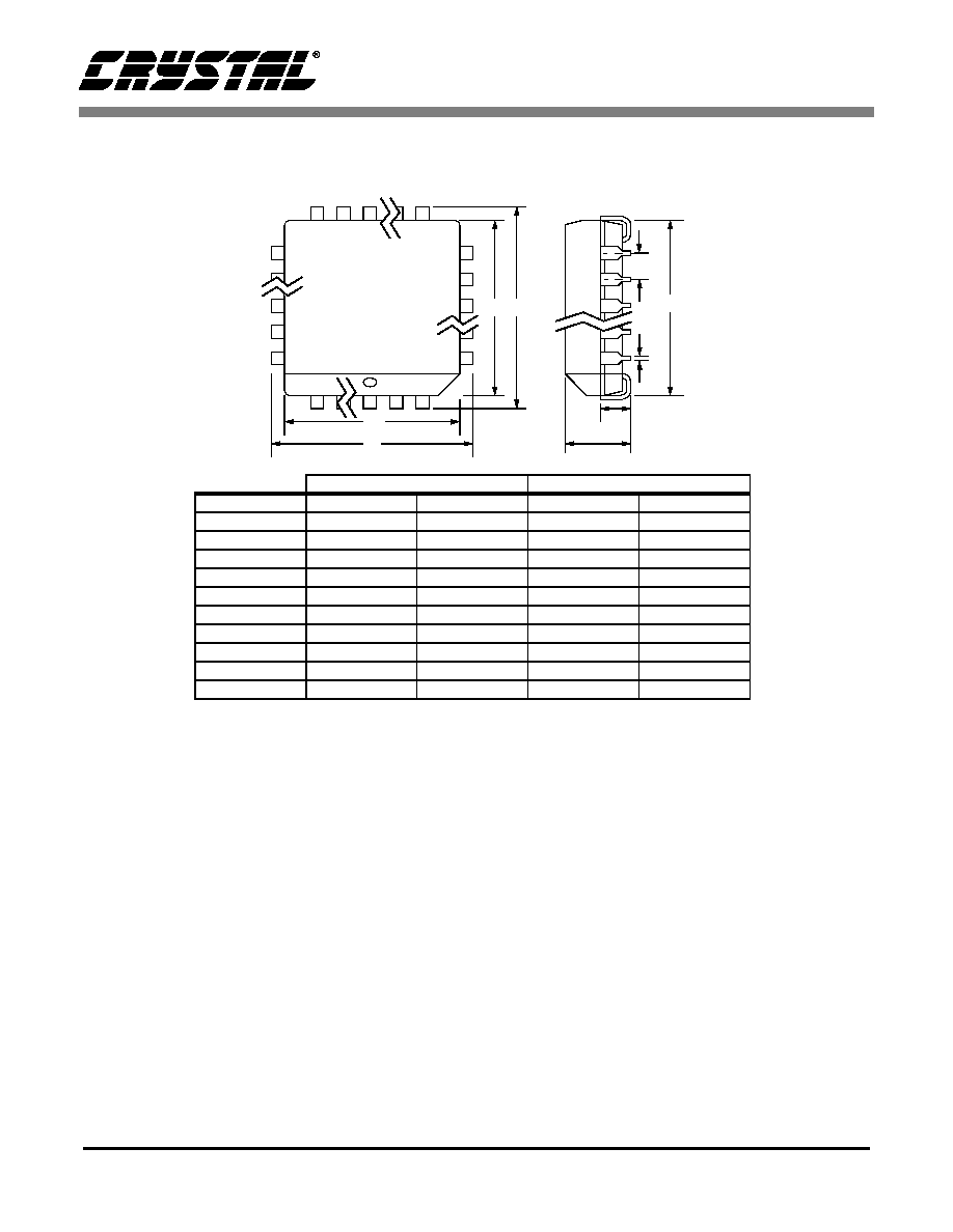
CS5320/21/22
36
DS454PP1
7. PACKAGE DIMENSIONS
INCHES
MILLIMETERS
DIM
MIN
MAX
MIN
MAX
A
0.165
0.180
4.043
4.572
A1
0.090
0.120
2.205
3.048
B
0.013
0.021
0.319
0.533
D
0.485
0.495
11.883
12.573
D1
0.450
0.456
11.025
11.582
D2
0.390
0.430
9.555
10.922
E
0.485
0.495
11.883
12.573
E1
0.450
0.456
11.025
11.582
E2
0.390
0.430
9.555
10.922
e
0.040
0.060
0.980
1.524
JEDEC #: MS-018
28L PLCC PACKAGE DRAWING
D1
D
E1 E
D2/E2
B
e
A1
A

· Notes ·
