
1
Features
s
Two Regulated Outputs
8V ±5%, 1A
5V ±5%, 250mA
s
Independent ENABLE for
each Output
s
Separate Sense Feedback
Lead for 8V Output
s
<10µA Sleep Mode Current
s
Fault Protection
Overvoltage Shutdown
+45V Peak Transient
Voltage
Short Circuit
Thermal Shutdown
s
CMOS Compatible, Low-
Current ENABLE Inputs
Package Options
TO-220 7 Lead
Tab (Gnd)
CS8371
8V/1A, 5V/250mA Dual Regulator with
Independent Output Enables and NoCapŞ
1
CS8371
Description
+
-
Pre-Regulator/
Bias Generator
Thermal
Shutdown
Trimmed Bandgap
Voltage Reference
ENABLE1
VCC
ENABLE2
Gnd
VOUT2
Sense
VOUT1
Overvoltage
Shutdown
-
+
+
-
Current Limit
+
-
VIA
Current Limit
1.2V
1.2V
Block Diagram
The CS8371 is a 8V/5V dual output
linear regulator. The 8V ±5% output
sources 1A, while the 5V ±5% out-
put sources 250mA. Each output is
controlled by its own ENABLE
lead. Setting the ENABLE input
high turns on the associated regula-
tor output. Holding both ENABLE
inputs low puts the IC into sleep
mode where current consumption
is less than 10µA.
The regulator is protected against
overvoltage, short-circuit and ther-
mal runaway conditions. The
device can withstand 45V load
dump transients making suitable
for use in automotive environ-
ments. CherryŐs proprietary
NoCapŞ solution is the first tech-
nology which allows the output to
be stable without the use of an
external capacitor.
The CS8371 is available in a 7 lead
TO-220 package with copper tab.
The tab can be connected to a
heatsink if necessary.
1 ENABLE
1
2 ENABLE
2
3 V
OUT2
4 Gnd
5 Sense
6 V
CC
7 V
OUT1
Rev. 6/9/99
Cherry Semiconductor Corporation
2000 South County Trail, East Greenwich, RI 02818
Tel: (401)885-3600 Fax: (401)885-5786
Email: info@cherry-semi.com
Web Site: www.cherry-semi.com
A Company
¨
NoCap is a trademark of Cherry Semiconductor Corporation, and is patented.

2
CS8371
PARAMETER
TEST CONDITIONS
MIN
TYP
MAX
UNIT
Electrical Characteristics: -40ˇC ˛ T
A
˛ +85ˇC, 10.5V ˛ V
CC
˛ 16.0V, ENABLE
1
= ENABLE
2
= 5.0V,
I
OUT1
= I
OUT2
= 5.0mA, unless otherwise stated.
s Primary Output (V
OUT1
)
Output Voltage
I
OUT1
= 1.0A
7.60
8.00
8.40
V
Line Regulation
10.5V ˛ V
CC
˛ 26V
50
mV
Load Regulation
5mA ˛ I
OUT1
˛ 1.0A
150
mV
Sleep Mode Quiescent
V
CC
= 14V, ENABLE
1
= ENABLE
2
= 0V
0
0.2
10.0
µA
Current
Quiescent Current
V
CC
= 14V, I
OUT1
= 1.0A, I
OUT2
= 250mA
30
mA
Dropout Voltage
I
OUT1
= 250mA
1.2
V
Dropout Voltage
I
OUT1
= 1.0A
1.5
V
Quiescent Bias Current
I
OUT1
= 5mA, ENABLE
2
= 0V, V
CC
= 14V
10
mA
I
Q
= I
CC
- I
OUT1
Quiescent Bias Current
I
OUT1
= 1.0A, ENABLE
2
= 0V, V
CC
= 14V
22
mA
I
Q
= I
CC
- I
OUT1
Ripple Rejection
f = 120Hz, V
CC
= 14V with 1.0V
PP
AC,
90
dB
C
OUT
= 0µF
f = 10kHz, V
CC
= 14V with 1.0V
PP
AC,
74
dB
C
OUT
= 0µF
f = 20kHz, V
CC
= 14V with 1.0V
PP
AC,
68
dB
C
OUT
= 0µF
Current Limit
V
CC
= 16V
1.1
2.5
A
Overshoot Voltage
5mA ˛ I
REG1
˛ 1.0A
6.0
V
Output Noise
10Hz-100kHz
300
µV
rms
s Secondary Output (V
OUT2
)
Output Voltage
I
OUT2
= 250mA
4.75
5.00
5.25
V
Line Regulation
7V ˛ V
CC
˛ 26V
40
mV
Load Regulation
5mA ˛ I
OUT2
˛ 250mA
100
mV
Dropout Voltage
I
OUT2
= 5.0mA
2.2
V
Dropout Voltage
I
OUT2
= 250mA
2.5
V
Quiescent Bias Current
I
OUT2
= 5mA, ENABLE
1
= 0V, V
CC
= 14V
7
mA
I
Q
= I
CC
- I
OUT2
Quiescent Bias Current
I
OUT2
= 250mA, ENABLE
1
= 0V, V
CC
= 14V
8
mA
I
Q
= I
CC
- I
OUT2
Ripple Rejection
f = 120Hz, V
CC
= 14V with 1.0 V
PP
AC,
90
dB
C
OUT
= 0µF
f= 10kHz, V
CC
= 14V with 1.0V
PP
AC,
75
dB
C
OUT
= 0µF
f = 20kHz, V
CC
= 14V with 1.0V
PP
AC,
67
dB
C
OUT
= 0µF
Absolute Maximum Ratings
Power Dissipation .............................................................................................................................................Internally Limited
ENABLE Input Voltage Range .............................................................................................................................-0.6V to +10.0V
Load Current (8V Regulator)...........................................................................................................................Internally Limited
Load Current (5V Regulator)...........................................................................................................................Internally Limited
Transient Peak Voltage (31V load dump @ 14V V
CC
) ...........................................................................................................45V
Storage Temperature Range ................................................................................................................................-65ˇC to +150ˇC
Junction Temperature Range...............................................................................................................................-40ˇC to +150ˇC
Lead Temperature Soldering: Wave Solder (through hole styles only) ..........................................10 sec. max, 260ˇC peak

3
Electrical Characteristics: -40ˇC ˛ T
A
˛ +85ˇC, 10.5V ˛ V
CC
˛ 16.0V, ENABLE
1
= ENABLE
2
= 5.0V,
I
OUT1
= I
OUT2
= 5.0mA, unless otherwise stated.
CS8371
Package Pin Description
PACKAGE PIN #
PIN SYMBOL
FUNCTION
7 Lead TO-220
1
ENABLE
1
ENABLE control for the 8V, 1A output
2
ENABLE
2
ENABLE control for the 5V, 250mA output
3
V
OUT2
5V ±5%, 250mA regulated output
4
Gnd
Ground
5
Sense
Sense feedback for the primary 8V output
6
V
CC
Supply voltage, usually from battery
7
V
OUT1
8V ±5%, 1A regulated output
PARAMETER
TEST CONDITIONS
MIN
TYP
MAX
UNIT
s Secondary Output (V
OUT2
): continued
Current Limit
V
CC
= 16V
270
600
mA
Overshoot Voltage
5mA ˛ I
REG2
˛ 250mA
4.3
V
Output Noise
10Hz-100kHz
170
µV
rms
s ENABLE Function (ENABLE)
Input Current
V
CC
= 14V, 0V ˛ ENABLE ˛ 5.5V
-150
150
µA
Input Voltage
Low
0
0.8
V
High
2.0
5.0
V
s Protection Circuitry
ESD Threshold
Human Body Model
±2.0
±4.0
kV
Overvoltage Shutdown
24
30
V
Thermal Shutdown
Guaranteed by Design
150
180
ˇC
Thermal Hysteresis
30
ˇC
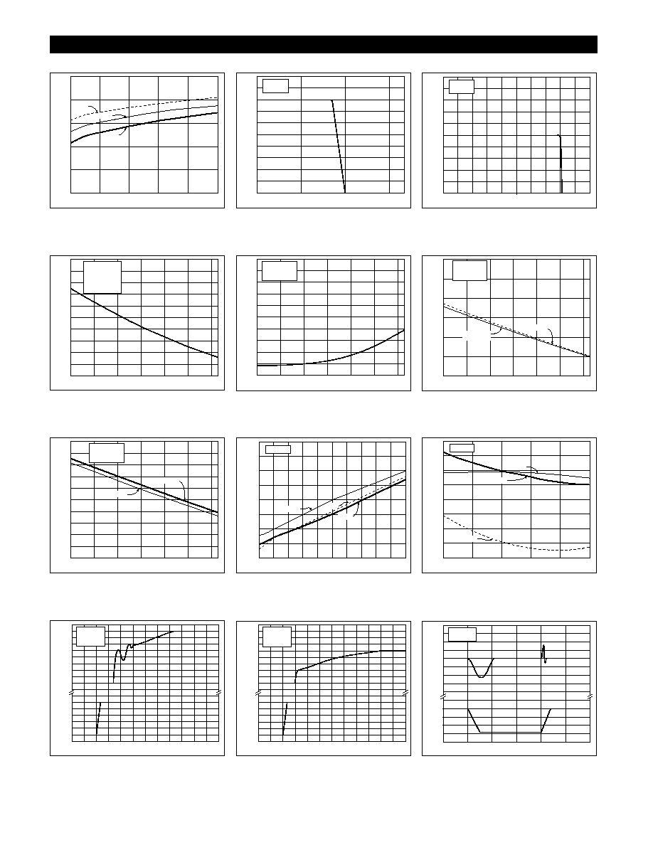
Typical Performance Characteristics
Output V
oltage (V)
8.05
8.04
8.03
8.02
8.01
8.00
7.99
7.98
7.97
7.96
7.95-40 -20
0
20
40
60
80
100
120
140
Ambient Temperature (
°C)
V
IN
= 14V
I
OUT
= 1A
Regulator 1 Output Voltage
Regulator 2 Output Voltage
Output V
oltage (V)
-40
-20
0
20
40
60
80
100
120
140
Ambient Temperature (
°C)
5.00
4.95
4.90
4.85
V
IN
= 14V
I
OUT
= 250A
Dropout V
oltage (V)
2.0
1.8
1.6
1.4
1.2
1.0
0.8
0.6
0.4
0.2
0
0
100
200
300
400
500
600
700
800
900
Output Current (mA)
1000
-40°C
25
°C
85
°C
Regulator 1 Dropout Voltage
4
CS8371
Typical Performance Characteristics: continued
Dropout V
oltage (V)
2.5
2.0
1.5
1.0
0.5
0
0
50
100
150
200
Output Current (mA)
250
-40°C
25
°C
85
°C
Regulator 2 Dropout Voltage
Regulator 1 Current Limit
Reg 1 Output V
oltage (V)
10
9
8
7
6
5
4
3
2
0 0
1
2
Reg 1 Output Current (A)
1
3
V
IN
= 14V
T
A
= 25
°C
Reg 2 Output V
oltage (V)
10
9
8
7
6
5
4
3
2
0
0
100
200
Reg 2 Output Current (mA)
1
300
V
IN
= 14V
T
A
= 25
°C
400
500
Regulator 2 Current Limit
Quiescent Current (mA)
9.0
8.5
8.0
7.5
7.0
6.5
6.0
5.5
5.0
4.5
4.0-40
-20
0
20
40
60
80
Ambient Temperature (
°C)
Enable 1 = 5V
Enable 2 = 5V
V
IN
= 14V
I
OUT
1 = 1A
I
OUT
2 = 250mA
Quiescent Current
Quiescent Current
Quiescent Current (
m
A)
1.0
0.9
0.8
0.7
0.6
0.5
0.4
0.3
0.2
0.1
0-40
-20
0
20
40
60
80
Ambient Temperature (
°C)
Enable 1 = 0V
Enable 2 = 0V
V
IN
= 14V
Quiescent Current (mA)
6.0
5.5
5.0
4.5
4.0
3.5
3.0-40
-20
0
20
40
60
80
Ambient Temperature (
°C)
I
OUT
= 5mA
I
OUT
= 1A
Enable 1 = 5V
Enable 2 = 0V
V
IN
= 14V
Regulator 1 Quiescent Current
Quiescent Current (mA)
4.0
3.8
3.6
3.4
3.2
3.0
2.8
2.6
2.4
2.2
2.0-40
-20
0
20
40
60
80
Ambient Temperature (
°C)
I
OUT
= 5mA
I
OUT
= 250mA
Enable 1 = 0V
Enable 2 = 5V
V
IN
= 14V
Regulator 2 Quiescent Current
Regulator 1 Load Regulation
Output V
oltage (V)
8.020
8.015
8.010
8.005
8.000
7.995
7.990
7.985
7.980
0
100
200
300
400
500
600
700
800
900
Output Current (mA)
1000
85
°C
25
°C
-40°C
V
IN
= 14V
Output V
oltage (V)
5.02
5.01
5.00
4.99
4.98
4.97
4.96
4.95
4.94
0
50
100
150
200
Output Current (mA)
250
-40°C
25
°C
85
°C
V
IN
= 14V
Regulator 2 Load Regulation
Enable 1 (V)
0
1
Time (
ms)
2
3
4
5
6
7
8
9
10
11
12
0
1
2
3
4
5
0
1
2
3
4
5
6
7
8
Reg 1 Output V
oltage (V)
C
OUT
= 0
mF
T
A
= 25
°C
I
OUT
= 5mA
Regulator 1 Startup
Regulator 2 Startup
Enable 2 (V)
0
1
Time (
ms)
2
3
4
5
6
7
8
9
10
11
12
0
1
2
3
4
5
0
1
2
3
4
5
6
7
8
Reg 2 Output V
oltage (V)
C
OUT
= 0
mF
T
A
= 25
°C
I
OUT
= 5mA
Output V
oltage Deviation (V)
2
1
0
-1
-2
16
14
12
10
0
100
200
300
400
500
Time (ns)
600
Input V
oltage (V)
C
OUT
= 0
mF
T
A
= 25
°C
Regulator 1 Line Transient Response

5
Typical Performance Characteristics: continued
CS8371
Output V
oltage Deviation (V)
0.4
0.2
0
-0.2
-0.4
16
14
12
10
0
100
200
300
400
500
Time (ns)
600
Input V
oltage (V)
-0.6
0.6
C
OUT
= 0
mF
T
A
= 25
°C
Regulator 2 Line Transient Response
Regulator 1 Load Transient Response
Output V
oltage Deviation (V)
2
1
0
-1
-2
1000
5
0
5
10
15
20
25
Time (
ms)
30
Load Current (mA)
-3
3
V
IN
= 14V
C
OUT
= 0
mF
T
A
= 25
°C
Output V
oltage Deviation (mV)
+500
0
-500
250
5
0
5
10
15
20
25
Time (
ms)
30
Load Current (mA)
V
IN
= 14V
C
OUT
= 0
mF
T
A
= 25
°C
Regulator 2 Load Transient Response
Ripple Rejection (dB)
100
80
60
40
20
1
10
100
1k
10k
100k
Frequency (Hz)
1M
T
A
= 25
°C
V
IN
= 14V
C
OUT
= 0
mF
Regulator 1 Ripple Rejection
Regulator 2 Ripple Rejection
Ripple Rejection (dB)
100
80
60
40
20
1
10
100
1k
10k
100k
Frequency (Hz)
1M
T
A
= 25
°C
V
IN
= 14V
C
OUT
= 0
mF
Output Capacitor ESR (
W
)
5
1
0.1
.01
0.1
1
10
100
1000
Output Capacitor Size (
mF)
Unstable
Region
T
A
= 25
°C
V
IN
= 14V
R
ESR
Ł 1.6W
I
OUT
= 5ma to 1A
Regulator 1 Stability
Definition of Terms
Dropout Voltage:
The input-output voltage differential at
which the circuit ceases to regulate against further
reduction in input voltage. Measured when the output
voltage has dropped 100mV from the nominal value
obtained at 14V input, dropout voltage is dependent
upon load current and junction temperature.
Current Limit:
Peak current that can be delivered to the output.
Input Voltage:
The DC voltage applied to the input terminals
with respect to ground.
Input Output Differential:
The voltage difference between the
unregulated input voltage and the regulated output
voltage for which the regulator will operate.
Line Regulation:
The change in output voltage for a change in
the input voltage. The measurement is made under
conditions of low dissipation or by using pulse tech-
niques such that the average chip temperature is not
significantly affected.
Load Regulation:
The change in output voltage for a change in
load current at constant chip temperature.
Long Term Stability:
Output voltage stability under accelerat-
ed life-test conditions after 1000 hours with maximum
rated voltage and junction temperature.
Output Noise Voltage:
The rms AC voltage at the output, with
constant load and no input ripple, measured over a
specified frequency range.
Quiescent Current:
The part of the positive input current that
does not contribute to the positive load current. The
regulator ground lead current.
Ripple Rejection:
The ratio of the peak-to-peak input ripple
voltage to the peak-to-peak output ripple voltage.
Temperature Stability of V
OUT
:
The percentage change in out-
put voltage for a thermal variation from room temper-
ature to either temperature extreme.