
PS9121
NEC's HIGH CMR, 15Mbps
OPEN COLLECTOR OUTPUT TYPE
5-PIN SOP 3.3V OPTOCOUPLER
California Eastern Laboratories
· LOW POWER CONSUMPTION:
V
CC
= 3.3 V
·
PULSE WIDTH DISTORTION:
|t
PHL
- t
PLH
| = 35 ns MAX.
· HIGH COMMON MODE TRANSIENT IMMUNITY:
CM
H
, CM
L
= ±15 kV/s MIN.
·
SMALL PACKAGE:
5-Pin SOP
·
HIGH SPEED:
15 Mbps
·
HIGH ISOLATION VOLTAGE:
BV = 2 500 V
r.m.s.
·
OPEN COLLECTOR OUTPUT
·
ORDERING NUMBER OF TAPING PRODUCT:
PS9121-1-F3, F4: 2 500 pcs/reel
·
Pb-Free Product
·
SAFETY STANDARDS:
UL approved: File No. E72422
DIN EN60747-5-2 (VDE0884 Part2) approved No. 40008902 (option)
FEATURES
DATA SHEET
NEC's PS9121 is an optically coupled high-speed, ac-
tive low type isolator containing a GaAlAs LED on the
input side and a photodiode and a signal processing
circuit on the output side on one chip.
NEC's PS9121 is designed specifically for high com-
mon mode transient immunity (CMR) and low pulse
width distortion. The PS9121 is suitable for high
density application.
DESCRIPTION
·
Measurement Equipment
·
PDP
·
FA Network
APPLICATION
TRUTH TABLE
LED
OUTPUT
ON
L
OFF
H
5
3
1
2
4
1. Anode
2. Cathode
3. GND
4. V
O
5. V
CC
PIN CONNECTION
(Top View)

PS9121
PACKAGE DIMENSIONS (UNIT: mm)
MARKING EXAMPLE
1.27
0.4
+0.10
-0.05
0.25 M
0.1±0.1
2.6±0.2
4.4
7.0±0.3
0.5±0.3
0.15
+0.10 -0.0
5
3.4
+0.3
-0.1
5
3
1
2
4
No. 1 pin Mark
Initial of NEC
(Engraved mark)
Rank Code
Year Assembled
(Last 1 Digit)
Week Assembled
N 3 45
Assembly Lot
9121
N 345
N
*1
*1 Bar : Pb-Free

PS9121
ORDERING INFORMATION
*1 For the application of the Safety Standard, following part number should be used.
*2 With regards to terminal solder (the solder contains lead) plated products (conventionally plated), contact your
nearby sales office.
ABSOLUTE MAXIMUM RATINGS
(T
A
=25şC, unless otherwise specified)
PART NUMBER
ORDER NUMBER
SOLDER PLATING
SPECIFICATION
PACKING STYLE
SAFETY STANDARDS
APPROVAL
APPLICATION
PART NUMBER
*1
PS9121
PS9121-A
Pb-Free*2
20 pcs (Tape 20 pcs cut) Standard products
(UL approved)
PS9121
PS9121-F3
PS9121-F3-A
Embossed Tape 2 500
pcs/reel
PS9121-F4
PS9121-F4-A
PS9121-V
PS9121-V-A
20 pcs (Tape 20 pcs cut) DIN EN60747-5-2
(VDE0884 Part2)
approved (Option)
PS9121-V-F3
PS9121-V-F3-A
Embossed Tape 2 500
pcs/reel
PS9121-V-F4
PS9121-V-F4-A
PARAMETER
SYMBOL
RATINGS
UNIT
Diode
Forward Current*1
I
F
30
mA
Reverse Voltage
V
R
5
V
Detector
Supply Voltage
V
CC
7
V
Output Voltage
V
O
7
V
Output Current
I
O
25
mA
Power Dissipation*2
P
C
40
mW
Isolation Voltage*3
BV
2 500
Vr.m.s.
Operating Ambient Temperature
T
A
-40 to +85
şC
Storage Temperature
T
stg
-55 to +125
şC
*1 Reduced to 0.3 mA/°C at T
A
= 25°C or more.
*2 Applies to output pin V
O
(collector pin). Reduced to 1.5 mW/°C at T
A
= 65°C or more.
*3 AC voltage for 1 minute at T
A
= 25°C, RH = 60% between input and output.
RECOMMENDED OPERATING CONDITIONS
PARAMETER
SYMBOL
MIN.
TYP.
MAX.
UNIT
Low Level Input Voltage
V
FL
0
0.8
V
High Level Input Current
I
FH
6.3
10
12.5
mA
Supply Voltage
V
CC
2.7
3.3
3.6
V
TTL (R
L
= 1 k, loads)
N
5
Pull-up Resistance
R
L
330
4 k

PS9121
ELECTRICAL CHARACTERISTICS
(T
A
= -40 to 85şC, unless otherwise specified)
PARAMETER
SYMBOL
CONDITIONS
MIN.
TYP.
*1
MAX.
UNIT
Diode
Forward Voltage
V
F
I
F
= 10 mA, T
A
= 25°C
1.4
1.65
1.8
V
Reverse Current
I
R
V
R
= 3 V, T
A
= 25°C
10
A
Terminal Capacitance
C
t
V = 0 V, f = 1 MHz, T
A
= 25°C
30
pF
Detector High Level Output Current
I
OH
V
CC
= V
O
= 3.3 V, V
F
= 0.8 V
1
80
A
V
CC
= V
O
= 5.5 V, V
F
= 0.8 V
1
*2
Low Level Output Voltage
*3
V
OL
V
CC
= 3.3 V, I
F
= 5 mA, I
OL
= 13 mA
0.2
0.6
V
V
CC
= 5.5 V, I
F
= 5 mA, I
OL
= 13 mA
0.2
*2
High Level Supply Current
I
CCH
V
CC
= 3.3 V, I
F
= 0 mA, V
O
= Open
4
7
mA
V
CC
= 5.5 V, I
F
= 0 mA, V
O
= Open
5
*2
Low Level Supply Current
I
CCL
V
CC
= 3.3 V, I
F
= 10 mA, V
O
= Open
7
10
V
CC
= 5.5 V, I
F
= 10 mA, V
O
= Open
9
*2
Coupled Threshold Input Current
(H L)
I
FHL
V
CC
= 3.3 V, V
O
= 0.8 V, R
L
= 350
2.5
5
V
CC
= 5 V, V
O
= 0.8 V, R
L
= 350
2.5
*2
Isolation Resistance
R
I-O
V
I-O
= 1 kV
DC
, RH = 40 to 60%,
T
A
= 25°C
10
11
Isolation Capacitance
C
I-O
V = 0 V, f = 1 MHz, T
A
= 25°C
0.6
pF
Propagation Delay Time
(H L)
*4
t
PHL
T
A
= 25°C
40
75
ns
V
CC
= 3.3 V, R
L
= 350 , I
F
= 7.5 mA
100
V
CC
= 5 V, R
L
= 350 , I
F
= 7.5 mA
37
*2
Propagation Delay Time
(L H)
*4
t
PLH
T
A
= 25°C
45
75
V
CC
= 3.3 V, R
L
= 350 , I
F
= 7.5 mA
100
V
CC
= 5 V, R
L
= 350 , I
F
= 7.5 mA
40
*2
Rise Time
t
r
V
CC
= 3.3 V, R
L
= 350 , I
F
= 7.5 mA
20
V
CC
= 5 V, R
L
= 350 , I
F
= 7.5 mA
20
*2
Fall Time
t
f
V
CC
= 3.3 V, R
L
= 350 , I
F
= 7.5 mA
5
V
CC
= 5 V, R
L
= 350 , I
F
= 7.5 mA
5
*2
Pulse Width Distortion
(PWD)
*4
| t
PHL-
t
PLH
|
V
CC
= 3.3 V, R
L
= 350 , I
F
= 7.5 mA
5
35
V
CC
= 5 V, R
L
= 350 , I
F
= 7.5 mA
3
*2
Propagation Delay Skew
t
PSK
V
CC
= 3.3 V, R
L
= 350 , I
F
= 7.5 mA
40
Common Mode
Transient Immunity at High
Level Output
*5
CM
H
V
CC
= 3.3 V, R
L
= 350 , T
A
= 25°C,
I
F
= 0 mA, V
O
> 2 V, V
CM
= 1 kV
15
20
kV/s
V
CC
= 5 V, R
L
= 350 , T
A
= 25°C,
I
F
= 0 mA, V
O
> 2 V, V
CM
= 1 kV
20
*2
Common Mode
Transient Immunity at Low
Level Output
*5
CM
L
V
CC
= 3.3 V, R
L
= 350 , T
A
= 25°C,
I
F
= 7.5 mA, V
O
< 0.8 V, V
CM
= 1 kV
15
20
V
CC
= 5 V, R
L
= 350 , T
A
= 25°C,
I
F
= 7.5 mA, V
O
< 0.8 V, V
CM
= 1 kV
20
*2

PS9121
*1 Typical values at T
A
= 25°C
*2 These values are reference values.
*3 Because V
OL
of 2 V or more may be output when LED current input and when output supply of V
CC
= 2.6 V or less, it is
important to confirm the characteristics (operation with the power supply on and off) during design, before using this device.
*4 Test circuit for propagation delay time
Remark C
L
includes probe and stray wiring capacitance.
*5 Test circuit for common mode transient immunity
Remark C
L
includes probe and stray wiring capacitance.
USAGE CAUTIONS
1. This product is weak for static electricity by designed with high-speed integrated circuit so protect against static electricity
when handling.
2. By-pass capacitor of 0.1 F is used between V
CC
and GND near device. Also, ensure that the distance between the leads of
the photocoupler and capacitor is no more than 10 mm.
Input
Output
1.5 V
V
OL
t
PHL
t
PLH
(I
F
= 7.5 mA)
50%
47
Pulse input (I
F
)
V
O
(monitor)
V
CC
= 3.3 V
Input
(monitor)
0.1 F
µ
C
L
= 15 pF
R
L
= 350
(PW = 1 s,
Duty cycle = 1/10)
µ
90%
10%
1 kV
0 V
V
OH
2 V
0.8 V
V
OL
V
CM
V
O
(I
F
= 0 mA)
V
O
(I
F
= 7.5 mA)
t
r
t
f
V
O
(monitor)
V
CC
= 3.3 V
0.1 F
µ
C
L
= 15 pF
SW
V
CM
I
F
R
L
= 350
PS9121
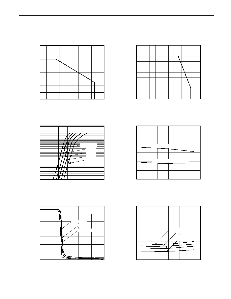
Remark The graphs indicate nominal characteristics.
TYPICAL CHARACTERISTICS
(T
A
= 25şC, unless otherwise specified)
20
40
60
80
100
0
85
10
20
30
40
1.0
0.01
0.1
1
10
100
1.2
1.4
1.6
1.8
2.0
2.2
2.4
T
A
= +85şC
+50şC
+25şC
0şC
-25şC
-50
-25
0
25
50
75
100
0
12
10
8
6
4
2
1
2
3
4
5
6
-50
-25
0
25
50
75
100
3.5
3
2.5
2
1.5
1
0.5
0
0.6
0.5
0.4
0.3
0.2
0.1
0
Ambient Temperature T
A
(şC)
Maximum Forward Current
I
F
(mA)
MAXIMUM FORWARD CURRENT
vs. AMBIENT TEMPERATURE
Forward Voltage V
F
(V)
Forward Current
I
F
(mA)
FORWARD CURRENT vs.
FORWARD VOLTAGE
Ambient Temperature T
A
(şC)
High Level Supply Current
I
CCH
(mA)
Low Level Supply Current
I
CCL
(mA)
SUPPLY CURRENT vs.
AMBIENT TEMPERATURE
Input Current I
F
(mA)
Output V
oltage
V
O
(V)
OUTPUT VOLTAGE vs. INPUT CURRENT
Ambient Temperature T
A
(şC)
Low Level Output V
oltage
V
OL
(V)
LOW LEVEL OUTPUT VOLTAGE vs.
AMBIENT TEMPERATURE
V
CC
= 3.3 V
4.0 k, 4.7 k
1.0 k
R
L
= 350
I
F
= 5.0 mA,
V
CC
= 3.3 V
13.0 mA
10.0 mA
6.0 mA
I
OL
= 16.0 mA
I
CCL
(V
CC
= 3.3 V, I
F
= 10 mA)
I
CCH
(V
CC
= 3.3 V, I
F
= 0 mA)
DETECTOR POWER DISSIPATION
vs. AMBIENT TEMPERATURE
Ambient Temperature T
A
(şC)
Detector Power Dissipation
P
C
(mW)
20
40
60
80
85
100
0
20
10
30
50
40

PS9121
5.0
4.0
3.0
2.0
1.0
0
100
80
60
40
20
0
120
100
80
60
40
20
0
-50
-25
0
25
50
75
100
-50
-25
0
25
50
75
100
-50
-25
0
25
50
75
100
15
13
11
9
7
5
-50
-25
0
25
50
75
100
300
250
200
150
100
50
0
120
100
80
60
40
20
0
THRESHOLD INPUT CURRENT vs.
AMBIENT TEMPERATURE
Ambient Temperature T
A
(şC)
Threshold Input Current
I
FHL
(mA)
Ambient Temperature T
A
(şC)
Propagation Delay T
ime
t
PHL
,
t
PLH
(ns)
PROPAGATION DELAY TIME vs.
AMBIENT TEMPERATURE
Ambient Temperature T
A
(şC)
Pulse Width Distortion
t
PHL
t
PLH
(ns)
PULSE WIDTH DISTORTION vs.
AMBIENT TEMPERATURE
Ambient Temperature T
A
(şC)
Switching T
ime
t
r
,
t
f
(ns)
SWITCHING TIME vs.
AMBIENT TEMPERATURE
Input Current I
F
(mA)
Propagation Delay T
ime
t
PHL
,
t
PLH
(ns)
PROPAGATION DELAY TIME vs.
INPUT CURRENT
1.0 k
R
L
= 350
4.0 k
V
CC
= 3.3 V,
V
O
= 0.6 V
R
L
= 4.7 k
R
L
= 4.0 k
R
L
= 350
R
L
= 1.0 k
I
F
= 7.5 mA,
V
CC
= 3.3 V
t
PLH
: R
L
= 4.0 k
t
PLH
: R
L
= 4.7 k
t
PLH
: R
L
= 1.0 k
t
PLH
: R
L
= 350
V
CC
= 3.3 V
t
PHL
: R
L
= 350 , 1.0 k, 4.0 k, 4.7 k
t
PHL
: R
L
= 350 , 1.0 k, 4.0 k, 4.7 k
t
PLH
: R
L
= 1.0 k
t
PLH
: R
L
= 350
t
PLH
: R
L
= 4.7 k
t
PLH
: R
L
= 4.0 k
I
F
= 7.5 mA,
V
CC
= 3.3 V
t
f
: R
L
= 350 , 1.0 k, 4.0 k, 4.7 k
t
r
: R
L
= 350
t
r
: R
L
= 1.0 k
t
r
: R
L
= 4.7 k
t
r
: R
L
= 4.0 k
I
F
= 7.5 mA,
V
CC
= 3.3 V
Remark The graphs indicate nominal characteristics.

PS9121
TAPING SPECIFICATIONS
(UNIT:mm)
Outline and Dimensions (Tape)
Tape Direction
PS9121-F3
PS9121-F4
Outline and Dimensions (Reel)
Packing: 2 500 pcs/reel
100±1.0
13.0±0.2
330±2.0
2.0±0.5
11.9 to 15.4
Outer edge of
flange
17.5±1.0
13.5±1.0
2.0±0.5
13.0±0.2
R 1.0
21.0±0.8
1.55±0.1
2.0±0.05
4.0±0.1
1.75±0.1
3.9±0.1
3.45 MAX.
7.4±0.1
0.3±0.05
8.0±0.1
1.5
+0.1
-0
5.5±0.1
12.0±0.2
3.0±0.1

PS9121
NOTES ON HANDLING
1. Recommended soldering conditions
(1) Infrared reflow soldering
· Peak reflow temperature
260°C or below (package surface temperature)
· Time of peak reflow temperature
10 seconds or less
· Time of temperature higher than 220°C
60 seconds or less
· Time to preheat temperature from 120 to 180°C 120±30 s
· Number of reflows
Three
· Flux
Rosin flux containing small amount of chlorine (The flux with a maximum
chlorine content of 0.2 Wt% is recommended.)
(2) Wave soldering
· Temperature
260°C or below (molten solder temperature)
· Time
10 seconds or less
· Preheating conditions 120°C or below (package surface temperature)
· Number of times
One (Allowed to be dipped in solder including plastic mold portion.)
· Flux
Rosin flux containing small amount of chlorine (The flux with a maximum chlorine content of 0.2
Wt% is recommended.)
(3) Soldering by Soldering Iron
· Peak Temperature (lead part temperature) 350°C or below
· Time (each pins)
3 seconds or less
· Flux
Rosin flux containing small amount of chlorine (The flux with a maximum
chlorine content of 0.2 Wt% is recommended.)
(a) Soldering of leads should be made at the point 1.5 to 2.0 mm from the root of the lead
(b) Please be sure that the temperature of the package would not be heated over 100°C
120±30 s
(preheating)
220şC
180şC
Package Surface T
emperature T
(şC)
Time (s)
Recommended Temperature Profile of Infrared Reflow
(heating)
to 10 s
to 60 s
260şC MAX.
120şC

PS9121
(4) Cautions
· Fluxes
Avoid removing the residual flux with freon-based and chlorine-based cleaning solvent.
2. Cautions regarding noise
Be aware that when voltage is applied suddenly between the photocoupler's input and output or between collector-emitters at
startup, the output transistor may enter the on state, even if the voltage is within the absolute maximum ratings.
USAGE CAUTIONS
1. Protect against static electricity when handling.
2. Avoid storage at a high temperature and high humidity.
Life Support Applications
These NEC products are not intended for use in life support devices, appliances, or systems where the malfunction of these products can reasonably
be expected to result in personal injury. The customers of CEL using or selling these products for use in such applications do so at their own risk and
agree to fully indemnify CEL for all damages resulting from such improper use or sale.
A Business Partner of NEC Compound Semiconductor Devices, Ltd.
04/05/2005