
® 2006 California Micro Devices Corp. All rights reserved.
03/15/06
490 N. McCarthy Blvd., Milpitas, CA 95035-5112
Tel: 408.263.3214
Fax: 408.263.7846
www.cmd.com
1
CM1470
PRELIMINARY
Praetorian
TM
4-, 6- and 8-Channel Series Inductor Networks
Features
Ę
Ultra-low capacitance filter results in excellent sig-
nal integrity
Ę
4, 6 and 8 channels of EMI filtering
Ę
0.4mm pitch Chip Scale Package (CSP)
Ę
▒2kV HBM Ł MIL-STD883 (Method 3015)
Ę
10 bump, 2.030mm x 0.836mm footprint CSP for
CM1470-04
Ę
14 bump, 2.830mm x 0.836mm footprint CSP for
CM1470-06
Ę
18 bump, 3.630mm x 0.836mm footprint CSP for
CM1470-08
Ę
OptiGuard
TM Coating for improved reliability at
assembly
Ę
Lead-free finishing
Applications
Ę
Data and control lines for high resolution camera
modules in phones
Ę
LCD modules
Ę
Mobile handsets
Ę
High-speed data I/O lines
Product Description
CMD's CM1470 is a family of series inductor networks
providing EMI filtering for applications that are
sensitive to signal integrity such as high-resolution
camera interfaces. The CM1470 is configured in 4, 6
and 8 channel formats. Each channel is implemented
as a single inductor element where the component
value is 17nH. The CM1470 will help suppress EMI
radiation to the external environment. The parts
integrate ESD diodes on every pin to provide
protection during the manufacturing process when the
device is placed on the PCB from a pick-and-place
machine. The ESD protection diodes safely dissipate
ESD strikes of
▒
2kV, per the MIL-STD-883 (Method
3015) specification for Human Body Model (HBM)
ESD.
This device is particularly well suited for portable
electronics (e.g. wireless handsets, PDAs) because of
its small package format and easy-to-use pin
assignments. In particular, the CM1470 is ideal for EMI
filtering data and control lines in camera modules
where it is placed near the transmission source on a
flexible PCB. The CM1470 level of performance (i.e.
cutoff frequency and attenuation level) can be tuned
with external signal trace capacitance.
The CM1470 incorporates OptiGuard
TM
which results in
improved reliability at assembly. The CM1470 is avail-
able in a space-saving, low-profile Chip Scale Package
with lead-free finishing
.
Electrical Schematic
1 of n Channels (n = 4, 6, 8)
17nH
3.2pF
3.2pF
B2 - B(n+1)
A(n+1)
B1
A1 - An

® 2006 California Micro Devices Corp. All rights reserved.
2
490 N. McCarthy Blvd., Milpitas, CA 95035-5112
Tel: 408.263.3214
Fax: 408.263.7846
www.cmd.com
03/15/06
CM1470
PRELIMINARY
PIN DESCRIPTIONS
PIN NUMBER
PIN
DESCRIPTION
PIN NUMBER
PIN
DESCRIPTION
-04
-06
-08
-04
-06
-08
A1
A1
A1
Inductor Input #1
B1
B1
B1
GND
A2
A2
A2
Inductor Input #2
B2
B2
B2
Inductor Input #1
A3
A3
A3
Inductor Input #3
B3
B3
B3
Inductor Input #2
A4
A4
A4
Inductor Input #4
B4
B4
B4
Inductor Input #3
A5
A5
Inductor Input #5
B5
B5
B5
Inductor Input #4
A6
A6
Inductor Input #6
B6
B6
Inductor Input #5
A7
Inductor Input #7
B7
B7
Inductor Input #6
A8
Inductor Input #8
B8
Inductor Input #7
A5
A7
A9
GND
B9
Inductor Input #8
147008
3
2
5
4
7
6
9
8
1
B
A
Orientation
Marking
N706
3
2
5
4
7
6
1
B
A
Orientation
Marking
N704
3
2
5
4
1
B
A
Orientation
Marking
A3
B3
A2
A1
B2
A5
B5
A4
B4
A7
B7
A6
B6
A9
B9
A8
B8
B1
A1
Orientation
Marking
A3
B3
A2
A1
B2
A5
B5
A4
B4
B1
A1
Orientation
Marking
A3
B3
A2
A1
B2
A5
B5
A4
B4
A7
B7
A6
B6
B1
A1
Orientation
Marking
CM1470-08CP
18-bump CSP
PACKAGE / PINOUT DIAGRAMS
Notes:
TOP VIEW
BOTTOM VIEW
(Bumps Down View)
(Bumps Up View)
1) These drawings are not to scale.
CM1470-04CP
10-bump CSP
CM1470-06CP
14-bump CSP
® 2006 California Micro Devices Corp. All rights reserved.
03/15/06
490 N. McCarthy Blvd., Milpitas, CA 95035-5112
Tel: 408.263.3214
Fax: 408.263.7846
www.cmd.com
3
CM1470
PRELIMINARY
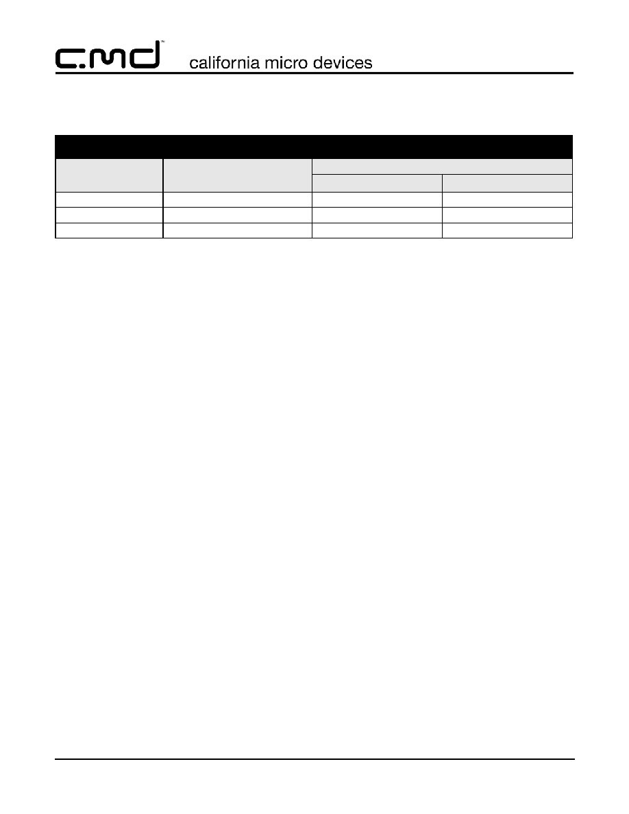
Ordering Information
Note 1: Parts are shipped in Tape & Reel form unless otherwise specified.
PART NUMBERING INFORMATION
Bumps
Package
Lead-free Finish
Ordering Part Number
1
Part Marking
10
CSP
CM1470-04CP
N704
14
CSP
CM1470-06CP
N706
18
CSP
CM1470-08CP
147008

® 2006 California Micro Devices Corp. All rights reserved.
4
490 N. McCarthy Blvd., Milpitas, CA 95035-5112
Tel: 408.263.3214
Fax: 408.263.7846
www.cmd.com
03/15/06
CM1470
PRELIMINARY
Specifications
Note 1: T
A
=25
░
C unless otherwise specified.
Note 2: ESD applied to input and output pins with respect to GND, one at a time.
Note 3: Clamping voltage is measured at the opposite side of the EMI filter to the ESD pin. For example, if ESD is applied to Pin A1,
then clamping voltage is measured at Pin B2.
Note 4: Unused pins are left open.
Note 5: These parameters are guaranteed by design and characterization.
ABSOLUTE MAXIMUM RATINGS
PARAMETER
RATING
UNITS
Storage Temperature Range
-65 to +150
░C
DC current per Inductor
30
mA
STANDARD OPERATING CONDITIONS
PARAMETER
RATING
UNITS
Operating Temperature Range
-40 to +85
░C
ELECTRICAL OPERATING CHARACTERISTICS
(NOTE 1
)
SYMBOL
PARAMETER
CONDITIONS
MIN
TYP
MAX
UNITS
L
TOT
Total Channel Inductance
17
nH
R
DC Channel Resistance
10
C
TOT
Total Channel Capacitance (C
1
x 2)
2.5V dc; 1MHz, 30mV ac
6.4
pF
C
1
Capacitance
2.5V dc; 1MHz, 30mV ac
3.2
pF
V
SIG
Signal Voltage
Positive Clamp
Negative Clamp
I
LOAD
= 10mA
5
-15
7
-10
15
-5
V
V
V
ST
Stand-off Voltage
I
= 10
A
6.0
V
I
LEAK
Diode Leakage Current
V
IN
=
+
3.3V
0.1
1.0
A
V
SIG
Signal Clamp Voltage
Positive Clamp
Negative Clamp
I
LOAD
= 10mA
I
LOAD
= -10mA
5.6
-1.5
6.8
-0.8
9.0
-0.4
V
V
V
ESD
In-system ESD Withstand Voltage
a) Human Body Model, MIL-STD-883,
Method 3015
b) Contact Discharge per IEC 61000-4-2
Level 4
Notes 2, 3, 4 and 5
▒4
▒2
kV
kV
f
C
Cut-off frequency
Z
SOURCE
= 50
, Z
LOAD
= 50
850
MHz

® 2006 California Micro Devices Corp. All rights reserved.
03/15/06
490 N. McCarthy Blvd., Milpitas, CA 95035-5112
Tel: 408.263.3214
Fax: 408.263.7846
www.cmd.com
5
CM1470
PRELIMINARY
Performance Information
Typical Filter Performance (nominal conditions unless specified otherwise, 50 Ohm Environment)
Figure 1. Insertion Loss VS. Frequency (A1-B2 to GND)
Figure 2. Typical Diode Capacitance vs. Input Voltage
(normalized to 2.5V d.c)

® 2006 California Micro Devices Corp. All rights reserved.
6
490 N. McCarthy Blvd., Milpitas, CA 95035-5112
Tel: 408.263.3214
Fax: 408.263.7846
www.cmd.com
03/15/06
CM1470
PRELIMINARY
Performance Information (cont'd)
Typical Filter Performance (nominal conditions unless specified otherwise, 50 Ohm Environment)
Figure 3. 2ns Rise and Fall Times of Clocked Signals at 25MHz, 50MHz and 100MHz
through CM1470 Inductor Array (Simulation)
25MHz
50MHz
75MHz

® 2006 California Micro Devices Corp. All rights reserved.
03/15/06
490 N. McCarthy Blvd., Milpitas, CA 95035-5112
Tel: 408.263.3214
Fax: 408.263.7846
www.cmd.com
7
CM1470
PRELIMINARY
Application Information
Refer to Application Note AP-217, "The Chip Scale Package", for a detailed description of Chip Scale Packages
offered by California Micro Devices.
Figure 4. Recommended Non-Solder Mask Defined Pad Illustration
Figure 5. Eutectic (SnPb) Solder
Ball Reflow Profile
Figure 6. Lead-free (SnAgCu) Solder
Ball Reflow Profile
PRINTED CIRCUIT BOARD RECOMMENDATIONS
PARAMETER
VALUE
Pad Size on PCB
0.240mm
Pad Shape
Round
Pad Definition
Non-Solder Mask defined pads
Solder Mask Opening
0.290mm Round
Solder Stencil Thickness
0.125 - 0.150mm
Solder Stencil Aperture Opening (laser cut, 5% tapered walls)
0.300mm Round
Solder Flux Ratio
50/50 by volume
Solder Paste Type
No Clean
Pad Protective Finish
OSP (Entek Cu Plus 106A)
Tolerance -- Edge To Corner Ball
+50
m
Solder Ball Side Coplanarity
+20
m
Maximum Dwell Time Above Liquidous
60 seconds
Maximum Soldering Temperature for Eutectic Devices using a Eutectic Solder Paste
240░C
Maximum Soldering Temperature for Lead-free Devices using a Lead-free Solder Paste
260░C
Solder Mask Opening
0.290mm DIA.
Non-Solder Mask Defined Pad
0.240mm DIA.
Solder Stencil Opening
0.300mm DIA.
200
250
150
100
50
0
1:00.0
2:00.0
3:00.0
4:00.0
Time (minutes)
T
emperature
(░
C)

® 2006 California Micro Devices Corp. All rights reserved.
8
490 N. McCarthy Blvd., Milpitas, CA 95035-5112
Tel: 408.263.3214
Fax: 408.263.7846
www.cmd.com
03/15/06
CM1470
PRELIMINARY
Mechanical Details
CM1470-04CP Mechanical Specifications
Dimensions for the CM1470-04CP supplied in a 10-
bump, 0.4mm pitch chip scale package (CSP) are pre-
sented below.
For complete information on the CSP-10, see the Cali-
fornia Micro Devices CSP Package Information docu-
ment.
Package Dimensions for
CM1470-04CP Chip Scale Package
PACKAGE DIMENSIONS
Package
Custom CSP
Bumps
10
Dim
Millimeters
Inches
Min
Nom
Max
Min
Nom
Max
A1
0.791 0.836 0.881 0.0311 0.0329 0.0347
A2
1.985 2.030 2.075 0.0781 0.0799 0.0817
B1
0.395 0.400 0.405 0.0156 0.0157 0.0159
B2
0.395 0.400 0.405 0.0156 0.0157 0.0159
C1
0.168 0.218 0.268 0.0066 0.0086 0.0106
C2
0.165 0.215 0.265 0.0065 0.0085 0.0104
D1
0.537 0.607 0.676 0.0211 0.0239 0.0266
D2
0.368 0.419 0.470 0.0145 0.0165 0.0185
# per tape and
reel
3500 pieces
Controlling dimension: millimeters
Mechanical Package Diagrams
0.25 DIA.
NOTE: DIMENSIONS IN MILLIMETERS
63/37 Sn/Pb (Eutectic) or
SOLDER BUMPS
96.8/2.6/0.6 Sn/Ag/Cu (Lead-free)
OptiGuard
TM
Coating
4
5
B
C1
B1
A1
B2
C2
D1
D2
A2
BOTTOM VIEW
SIDE
VIEW
A
1
2
3
A
B
OptiGuard
TM
Coated CSP

® 2006 California Micro Devices Corp. All rights reserved.
03/15/06
490 N. McCarthy Blvd., Milpitas, CA 95035-5112
Tel: 408.263.3214
Fax: 408.263.7846
www.cmd.com
9
CM1470
PRELIMINARY
Mechanical Details
CM1470-06CP Mechanical Specifications
Dimensions for the CM1470-04CP supplied in a 14-
bump, 0.4mm pitch chip scale package (CSP) are pre-
sented below.
For complete information on the CSP-14, see the Cali-
fornia Micro Devices CSP Package Information docu-
ment.
Package Dimensions for
CM1470-06CP Chip Scale Package
PACKAGE DIMENSIONS
Package
Custom CSP
Bumps
14
Dim
Millimeters
Inches
Min
Nom
Max
Min
Nom
Max
A1
0.791 0.836 0.881 0.0311 0.0329 0.0347
A2
2.785 2.830 2.875 0.1096 0.1114 0.1132
B1
0.395 0.400 0.405 0.0156 0.0157 0.0159
B2
0.395 0.400 0.405 0.0156 0.0157 0.0159
C1
0.168 0.218 0.268 0.0066 0.0086 0.0106
C2
0.165 0.215 0.265 0.0065 0.0085 0.0104
D1
0.537 0.607 0.676 0.0211 0.0239 0.0266
D2
0.368 0.419 0.470 0.0145 0.0165 0.0185
# per tape and
reel
3500 pieces
Controlling dimension: millimeters
Mechanical Package Diagrams
NOTE: DIMENSIONS IN MILLIMETERS
OptiGuard
TM
Coated CSP
0.25 DIA.
63/37 Sn/Pb (Eutectic) or
SOLDER BUMPS
96.8/2.6/0.6 Sn/Ag/Cu (Lead-free)
OptiGuard
TM
Coating
4
5
B
C1
B1
A1
B2
C2
D1
D2
A2
BOTTOM VIEW
SIDE
VIEW
A
1
2
3
A
B
A
B
6
7

® 2006 California Micro Devices Corp. All rights reserved.
10
490 N. McCarthy Blvd., Milpitas, CA 95035-5112
Tel: 408.263.3214
Fax: 408.263.7846
www.cmd.com
03/15/06
CM1470
PRELIMINARY
Mechanical Details
CM1470-08CP Mechanical Specifications
Dimensions for the CM1470-08CP supplied in an 18-
bump, 0.4mm pitch chip scale package (CSP) are pre-
sented below.
For complete information on the CSP-18, see the Cali-
fornia Micro Devices CSP Package Information docu-
ment.
Package Dimensions for
CM1470-08CP Chip Scale Package
PACKAGE DIMENSIONS
Package
Custom CSP
Bumps
18
Dim
Millimeters
Inches
Min
Nom
Max
Min
Nom
Max
A1
0.791 0.836 0.881 0.0311 0.0329 0.0347
A2
3.585 3.630 3.675 0.1411 0.1429 0.1447
B1
0.395 0.400 0.405 0.0156 0.0157 0.0159
B2
0.395 0.400 0.405 0.0156 0.0157 0.0159
C1
0.168 0.218 0.268 0.0066 0.0086 0.0106
C2
0.165 0.215 0.265 0.0065 0.0085 0.0104
D1
0.537 0.607 0.676 0.0211 0.0239 0.0266
D2
0.368 0.419 0.470 0.0145 0.0165 0.0185
# per tape and
reel
3500 pieces
Controlling dimension: millimeters
Mechanical Package Diagrams
NOTE: DIMENSIONS IN MILLIMETERS
OptiGuard
TM
Coated CSP
0.25 DIA.
63/37 Sn/Pb (Eutectic) or
SOLDER BUMPS
96.8/2.6/0.6 Sn/Ag/Cu (Lead-free)
OptiGuard
TM
Coating
4
5
B
C1
B1
A1
B2
C2
D1
D2
A2
BOTTOM VIEW
SIDE
VIEW
A
1
2
3
A
B
A
B
6
7
8
9

® 2006 California Micro Devices Corp. All rights reserved.
03/15/06
490 N. McCarthy Blvd., Milpitas, CA 95035-5112
Tel: 408.263.3214
Fax: 408.263.7846
www.cmd.com
11
CM1470
PRELIMINARY
CSP Tape and Reel Specifications
Figure 7. Tape and Reel Mechanical Data
PART NUMBER
CHIP SIZE (mm)
POCKET SIZE (mm)
B
0
X A
0
X K
0
TAPE WIDTH
W
REEL
DIAMETER
QTY PER
REEL
P
0
P
1
CM1470-04CP
2.03 X 0.836 X 0.644
2.17 x 1.12 x 0.71
8mm
178mm (7")
3500
4mm
4mm
CM1470-06CP
2.83 X 0.836 X 0.644
2.97 x 0.97 x 0.74
8mm
178mm (7")
3500
4mm
4mm
CM1470-08CP
3.63 X 0.836 X 0.644
3.76 x 0.97 x 0.74
8mm
178mm (7")
3500
4mm
4mm
Top
For Tape Feeder Reference
Cover
Tape
P
1
Only including Draft.
Concentric Around B.
K
o
Embossment
User Direction of Feed
▒
0.2 mm
P
o
Center Lines
of Cavity
W
10 Pitches Cumulative
Tolerance On Tape
A
o
B
o