Äîêóìåíòàöèÿ è îïèñàíèÿ www.docs.chipfind.ru
®
MPY634
1
FEATURES
q
WIDE BANDWIDTH: 10MHz typ
q
±
0.5% MAX FOUR-QUADRANT
ACCURACY
q
INTERNAL WIDE-BANDWIDTH OP AMP
q
EASY TO USE
q
LOW COST
APPLICATIONS
q
PRECISION ANALOG SIGNAL
PROCESSING
q
MODULATION AND DEMODULATION
q
VOLTAGE-CONTROLLED AMPLIFIERS
q
VIDEO SIGNAL PROCESSING
q
VOLTAGE-CONTROLLED FILTERS AND
OSCILLATORS
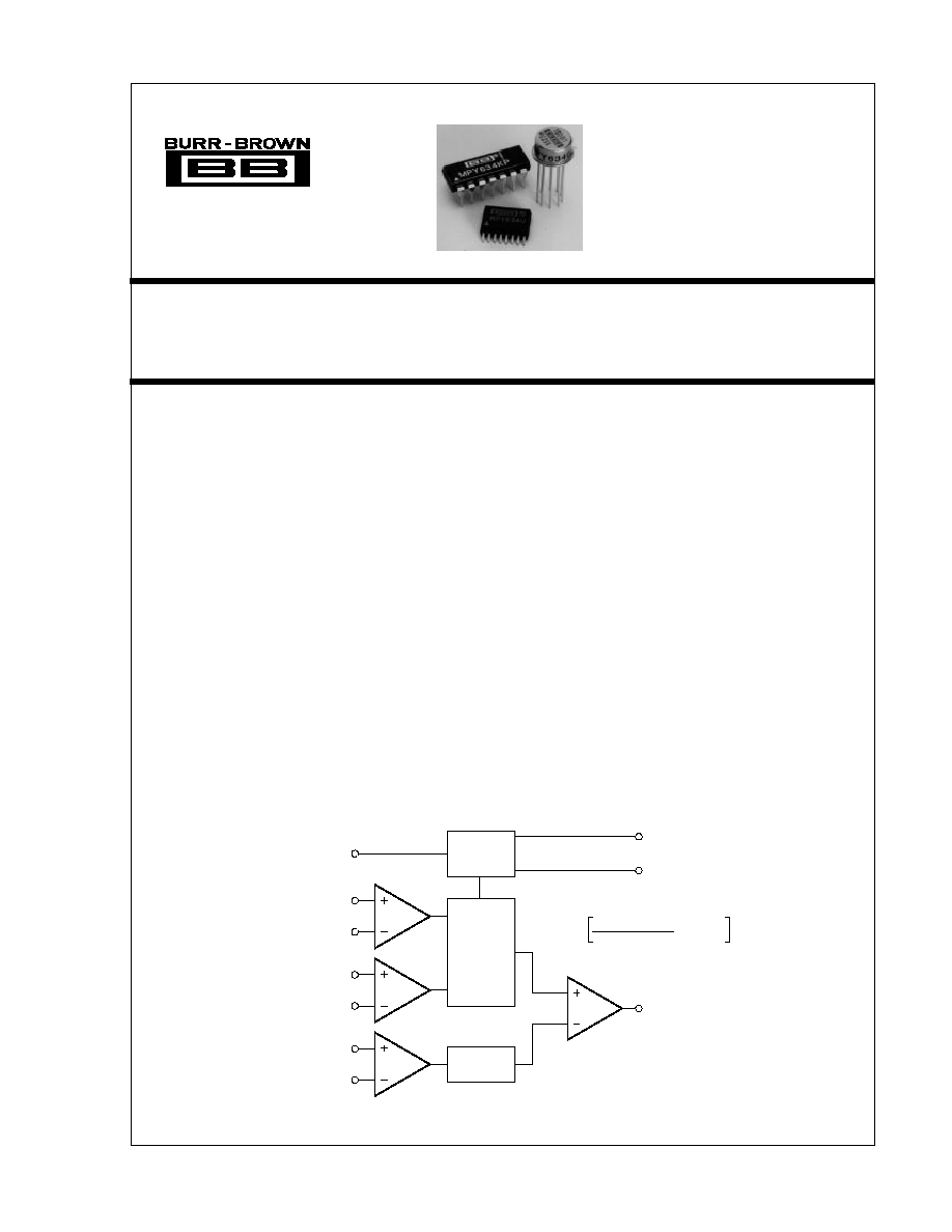
DESCRIPTION
The MPY634 is a wide bandwidth, high accuracy,
four-quadrant analog multiplier. Its accurately laser-
trimmed multiplier characteristics make it easy to use
in a wide variety of applications with a minimum of
external parts, often eliminating all external trimming.
Its differential X, Y, and Z inputs allow configuration
as a multiplier, squarer, divider, square-rooter, and
other functions while maintaining high accuracy.
The wide bandwidth of this new design allows signal
processing at IF, RF, and video frequencies. The
internal output amplifier of the MPY634 reduces
design complexity compared to other high frequency
multipliers and balanced modulator circuits. It is
capable of performing frequency mixing, balanced
modulation, and demodulation with excellent carrier
rejection.
An accurate internal voltage reference provides
precise setting of the scale factor. The differential Z
input allows user-selected scale factors from 0.1 to 10
using external feedback resistors.
V-I
X
1
X
2
Y
1
Y
2
Z
1
Z
2
V-I
V-I
SF
Multiplier
Core
Voltage
Reference
and Bias
0.75 Atten
A
V
OUT
V
S
+V
S
(X
1
X
2
)(Y
1
Y
2
)
SF
V
OUT
= A (Z
1
Z
2
)
Transfer Function
Precision
Output
Op Amp
MPY634
International Airport Industrial Park · Mailing Address: PO Box 11400 · Tucson, AZ 85734 · Street Address: 6730 S. Tucson Blvd. · Tucson, AZ 85706
Tel: (520) 746-1111 · Twx: 910-952-1111 · Cable: BBRCORP · Telex: 066-6491 · FAX: (520) 889-1510 · Immediate Product Info: (800) 548-6132
©
1985 Burr-Brown Corporation
PDS-636D
Printed in U.S.A. December, 1995
®
Wide Bandwidth
PRECISION ANALOG MULTIPLIER
®
MPY634
2
SPECIFICATIONS
ELECTRICAL
At T
A
= +25
°
C and V
S
=
±
15VDC, unless otherwise noted.
MPY634KP/KU
MPY634AM
MPY634BM
MPY634SM
(Z
2
Z
1
)
(X
1
X
2
)
10V + Y
1
(X
1
X
2
) (Y
1
Y
2
)
10V
+ Z
2
(X
1
X
2
)
2
+ Z
2
10V
MODEL
MIN
TYP
MAX
MIN
TYP
MAX
MIN
TYP
MAX
MIN
TYP
MAX
UNITS
MULTIPLIER
PERFORMANCE
Transfer Function
*
*
*
Total Error
(1)
(10V
X, Y
+10V)
±
2.0
±
1.0
±
0.5
*
%
T
A
= min to max
±
2.5
±
1.5
±
1.0
±
2.0
%
Total Error vs Temperature
±
0.03
±
0.022
±
0.015
±
0.02
%/
°
C
Scale Factor Error
(SF = 10.000V Nominal)
(2)
±
0.25
±
0.1
*
*
%
Temperature Coefficient of
Scaling Voltage
±
0.02
±
0.01
±
0.01
*
%/
°
C
Supply Rejection (
±
15V
±
1V)
*
±
0.01
*
*
%
Nonlinearity
X (X = 20Vp-p, Y = 10V)
*
±
0.4
0.2
±
0.3
*
%
Y (Y = 20Vp-p, X = 10V)
*
±
0.01
*
±
0.1
*
%
Feedthrough
(3)
X (Y Nulled, X = 20Vp-p, 50Hz)
*
±
0.3
±
0.15
±
0.3
*
%
Y (X Nulled, Y = 20Vp-p, 50Hz)
*
±
0.01
*
±
0.1
*
%
Both Inputs (500kHz, 1Vrms)
Unnulled
40
(4)
50
45
55
*
60
*
*
dB
Nulled
55
(4)
60
55
65
60
70
*
*
dB
Output Offset Voltage
±
50
±
100
±
5
±
30
*
±
15
*
*
mV
Output Offset Voltage Drift
*
±
200
±
100
*
±
500
µ
V/
°
C
DYNAMICS
Small Signal BW,
(V
OUT
= 0.1Vrms)
6
(4)
*
8
10
*
*
6
*
MHz
1% Amplitude Error
(C
LOAD
= 1000pF)
*
100
*
*
kHz
Slew Rate (V
OUT
= 20Vp-p)
*
20
*
*
V/
µ
s
Settling Time
(to 1%,
V
OUT
= 20V)
*
2
*
*
µ
s
NOISE
Noise Spectral Density:
SF = 10V
*
0.8
*
*
µ
V/
Hz
Wideband Noise:
f = 10Hz to 5MHz
*
1
*
*
mVrms
f = 10Hz to 10kHz
*
90
*
*
µ
Vrms
OUTPUT
Output Voltage Swing
*
±
11
*
*
V
Output Impedance (f
1kHz)
*
0.1
*
*
Output Short Circuit Current
(R
L
= 0, T
A
= min to max)
*
30
*
*
mA
Amplifier Open Loop Gain
(f = 50Hz)
*
85
*
*
dB
INPUT AMPLIFIERS (X, Y and Z)
Input Voltage Range
Differential V
IN
(V
CM
= 0)
*
±
12
*
*
V
Common-Mode V
IN
(V
DIFF
= 0)
*
±
10
*
*
V
(see Typical Performance Curves)
Offset Voltage X, Y
±
25
±
100
±
5
±
20
±
2
±
10
*
*
mV
Offset Voltage Drift X, Y
200
100
50
*
µ
V/
°
C
Offset Voltage Z
±
25
±
100
±
5
±
30
±
2
±
15
*
*
mV
Offset Voltage Drift Z
*
200
100
500
µ
V/
°
C
CMRR
*
*
60
80
70
90
*
*
dB
Bias Current
*
*
0.8
2.0
*
*
*
*
µ
A
Offset Current
*
0.1
*
*
2.0
µ
A
Differential Resistance
*
10
*
*
M
DIVIDER PERFORMANCE
Transfer Function (X
1
> X
2
)
*
*
*
Total Error
(1)
untrimmed
(X = 10V, 10V
Z
+10V)
1.5
±
0.75
±
0.35
±
0.75
%
(X = 1V, 1V
Z
+1V)
4.0
±
2.0
±
1.0
*
%
(0.1V
X
10V, 10V
Z
10V)
5.0
±
2.5
±
1.0
*
%
SQUARE PERFORMANCE
Transfer Function
*
*
*
Total Error (10V
X
10V)
±
1.2
±
0.6
±
0.3
*
%
®
MPY634
3
SQUARE-ROOTER
PERFORMANCE
Transfer Function (Z
1
Z
2
)
*
*
*
Total Error
(1)
(1V
Z
10V)
±
2.0
±
1.0
±
0.5
*
%
POWER SUPPLY
Supply Voltage:
Rated Performance
*
±
15
*
*
VDC
Operating
*
*
±
8
±
18
*
*
*
±
20
VDC
Supply Current, Quiescent
*
*
4
6
*
*
*
*
mA
TEMPERATURE RANGE
Specification
*
(5)
*
(5)
25
+85
*
*
55
+125
°
C
Storage
40
+85
65
+150
*
*
*
*
°
C
10
1
5
3
4
X
1
V
S
Y
2
Y
1
SF
X
2
2
SOIC: MPY634KU
DIP: MPY634KP
TO-100: MPY634AM/BM/SM
9
8
7
6
Z
2
Z
1
Out
+V
S
1
2
3
4
5
6
7
14
13
12
11
10
9
8
X
1
Input
X
2
Input
NC
Scale Factor
NC
Y
1
Input
Y
2
Input
+V
S
NC
Output
Z
1
Input
Z
2
Input
NC
V
S
1
2
3
4
5
6
7
8
16
15
14
13
12
11
10
9
X
1
Input
X
2
Input
NC
Scale Factor
NC
Y
1
Input
Y
2
Input
NC
+V
S
NC
Output
Z
1
Input
Z
2
Input
NC
V
S
NC
SPECIFICATIONS
(
CONT
)
ELECTRICAL
At T
A
= +25
°
C and V
S
=
±
15VDC, unless otherwise noted.
MPY634KP/KU
MPY634AM
MPY634BM
MPY634SM
MODEL
MIN
TYP
MAX
MIN
TYP
MAX
MIN
TYP
MAX
MIN
TYP
MAX
UNITS
10V (Z
2
Z
1
) +X
2
* Specification same as for MPY634AM.
NOTES: (1) Figures given are percent of full scale,
±
10V (i.e., 0.01% = 1mV). (2) May be reduced to 3V using external resistor between V
S
and SF. (3) Irreducible
component due to nonlinearity; excludes effect of offsets. (4) KP grade only. (5) KP grade only. 0
°
C to +70
°
C for KU grade.
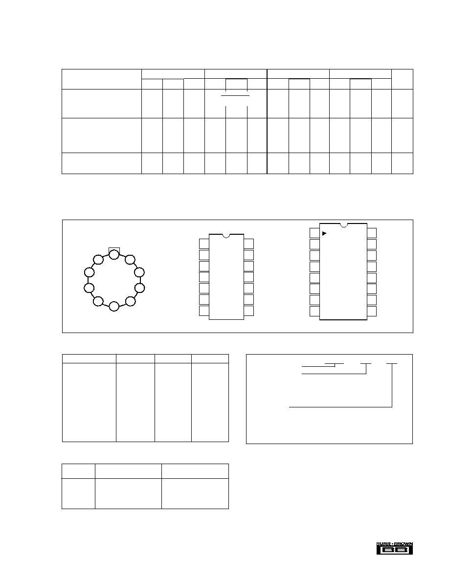
PIN CONFIGURATIONS
ABSOLUTE MAXIMUM RATINGS
PARAMETER
MPY634AM/BM MPY634KP/KU
MPY634SM
Power Supply Voltage
±
18
*
±
20
Power Dissipation
500mW
*
*
Output Short-Circuit
to Ground
Indefinite
*
*
Input Voltage ( all X,
Y and Z)
±
V
S
*
*
Temperature Range:
Operating
25
°
C/+85
°
C
*
55
°
C/+125
°
C
Storage
65
°
C/+150
°
C
40
°
C/+85
°
C
*
Lead Temperature
(soldering, 10s)
+300
°
C
*
*
SOIC `KU' Package
+260
°
C
* Specification same as for MPY634AM/BM.
Basic Model Number
Performance Grade
(1)
K: 25
°
C to +85
°
C (`U' package 0
°
C to +70
°
C)
A: 25
°
C to +85
°
C
B: 25
°
C to +85
°
C
S: 55
°
C to +125
°
C
Package Code
M: TO-100 Metal
P: Plastic 14-pin DIP
U: 16-pin SOIC
NOTE: (1) Performance grade identifier may not be marked on the SOIC
package; a blank denotes "K" grade.
ORDERING INFORMATION
MPY634
( )
( )
Top View
PACKAGE DRAWING
MODEL
PACKAGE
NUMBER
(1)
MPY634KP
14-Pin PDIP
010
MPY634KU
16-Pin SOIC
211
MPY634AM
TO-100
007
MPY634BM
TO-100
007
MPY634SM
TO-100
007
NOTE: (1) For detailed drawing and dimension table, please see end of data
sheet, or Appendix D of Burr-Brown IC Data Book.
PACKAGE INFORMATION
®
MPY634
4
TYPICAL PERFORMANCE CURVES
T
A
= +25
°
C, V
S
=
±
15VDC, unless otherwise noted.
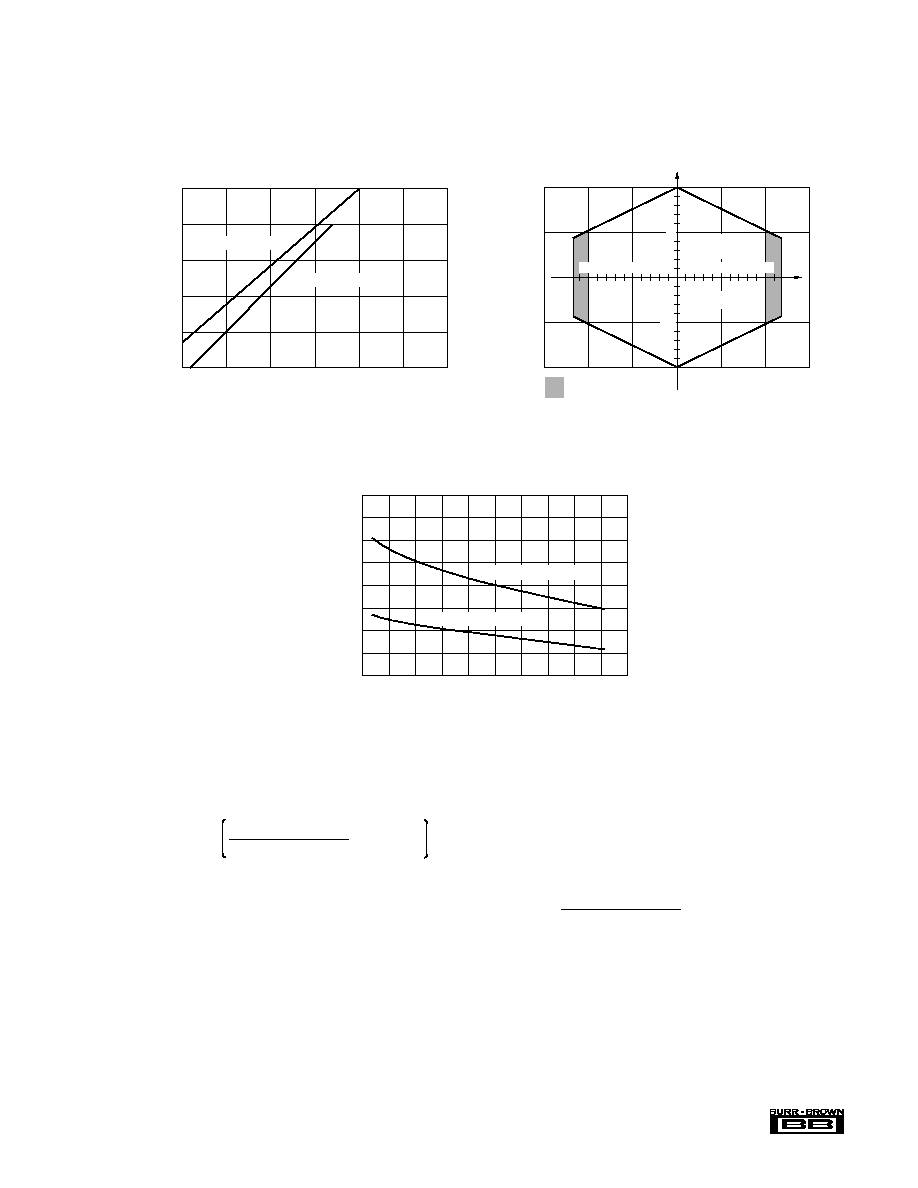
20
40
60
80
100
100
1k
10k
1M
10M
100M
Frequency (Hz)
FEEDTHROUGH vs FREQUENCY
Feedthrough Attenuation (dB)
100k
X Feedthrough
Y Feedthrough
10
0
10
20
30
1k
10k
100k
1M
10M
100M
Frequency (Hz)
FREQUENCY RESPONSE AS A MULTIPLIER
Output Response (dB)
C
L
= 0pF
C
L
= 1000pF
Normal Connection
With
X
10 Feedback
Attenuator
90
80
70
60
50
40
30
20
10
0
10k
1M
10M
Frequency (Hz)
COMMON-MODE REJECTION RATIO vs FREQUENCY
CMRR (dB)
100
100M
Typical for all inputs
50
60
70
80
Temperature (°C)
FEEDTHROUGH vs TEMPERATURE
Feedthrough Attenuation (dB)
20
20
60
100
140
40
0
40
80
120
f
Y
= 500kHz
V
X
= nulled
nulled at 25°C
60
1.5
1.25
1
0.75
0.5
10
100
10k
100k
Frequency (Hz)
NOISE SPECTRAL DENSITY
vs FREQUENCY
Noise Spectral Density (
µ
V/
Hz)
1k
60
40
20
0
20
1k
10k
100k
1M
10M
100M
Frequency (Hz)
FREQUENCY RESPONSE AS A DIVIDER
Output, V
0
/V
2
(dB)
V
X
= 100mVDC
V
Z
= 10mVrms
V
X
= 1VDC
V
Z
= 100mVrms
V
X
= 10VDC
V
Z
= 100mVrms
The information provided herein is believed to be reliable; however, BURR-BROWN assumes no responsibility for inaccuracies or omissions. BURR-BROWN
assumes no responsibility for the use of this information, and all use of such information shall be entirely at the user's own risk. Prices and specifications are subject
to change without notice. No patent rights or licenses to any of the circuits described herein are implied or granted to any third party. BURR-BROWN does not
authorize or warrant any BURR-BROWN product for use in life support devices and/or systems.
®
MPY634
5
inspection of the transfer function reveals that any V
OUT
can
be created with an infinitesimally small quantity within the
brackets. Then, an application circuit can be analyzed by
assigning circuit voltages for all X, Y and Z inputs and
setting the bracketed quantity equal to zero. For example,
the basic multiplier connection in Figure 1, Z
1
= V
OUT
and
Z
2
= 0. The quantity within the brackets then reduces to:
(V
OUT
0) = 0
This approach leads to a simple relationship which can be
solved for V
OUT
to provide the closed-loop transfer function.
The scale factor is accurately factory adjusted to 10V and is
typically accurate to within 0.1% or less. The scale factor
may be adjusted by connecting a resistor or potentiometer
between pin SF and the V
S
power supply. The value of the
external resistor can be approximated by:
TYPICAL PERFORMANCE CURVES
(CONT)
T
A
= +25
°
C, V
S
=
±
15VDC, unless otherwise noted.
THEORY OF OPERATION
The transfer function for the MPY634 is:
V
OUT
= A (Z
1
Z
2
)
where:
A = open-loop gain of the output amplifier (typically
85dB at DC).
SF = Scale Factor. Laser-trimmed to 10V but adjustable
over a 3V to 10V range using external resistors.
X, Y, Z are input voltages. Full-scale input voltage
is equal to the selected SF. (Max input voltage =
±
1.25 SF).
An intuitive understanding of transfer function can be gained
by analogy to the op amp. By assuming that the open-loop
gain, A, of the output operational amplifier is infinite,
(X
1
X
2
) (Y
1
Y
2
)
SF
(X
1
X
2
) (Y
1
Y
2
)
SF
10
INPUT DIFFERENTIAL-MODE/
COMMON-MODE VOLTAGE
12
12
10
5
5
5
5
10
10
Specified
Accuracy
V
S
= ±15V
Functional
Derated Accuracy
V
CM
V
DIFF
14
12
10
8
6
4
8
10
12
16
18
20
Positive or Negative Supply (V)
INPUT/OUTPUT SIGNAL RANGE
vs SUPPLY VOLTAGES
Peak Positive or Negative Signal (V)
14
Output, R
L
2k
All inputs, SF = 10V
800
700
600
500
400
300
200
100
0
20
0
60
100
140
Temperature (°C)
BIAS CURRENTS vs TEMPERATURE
(X,Y or Z Inputs)
Bias Current (nA)
20
40
40
80
120
Scaling Voltage = 10V
Scaling Voltage = 3V
60