Äîêóìåíòàöèÿ è îïèñàíèÿ www.docs.chipfind.ru
ISO485
ISO485
Isolated RS-485
DIFFERENTIAL BUS TRANSCEIVER
International Airport Industrial Park · Mailing Address: PO Box 11400 · Tucson, AZ 85734 · Street Address: 6730 S. Tucson Blvd. · Tucson, AZ 85706
Tel: (520) 746-1111 · Twx: 910-952-1111 · Cable: BBRCORP · Telex: 066-6491 · FAX: (520) 889-1510 · Immediate Product Info: (800) 548-6132
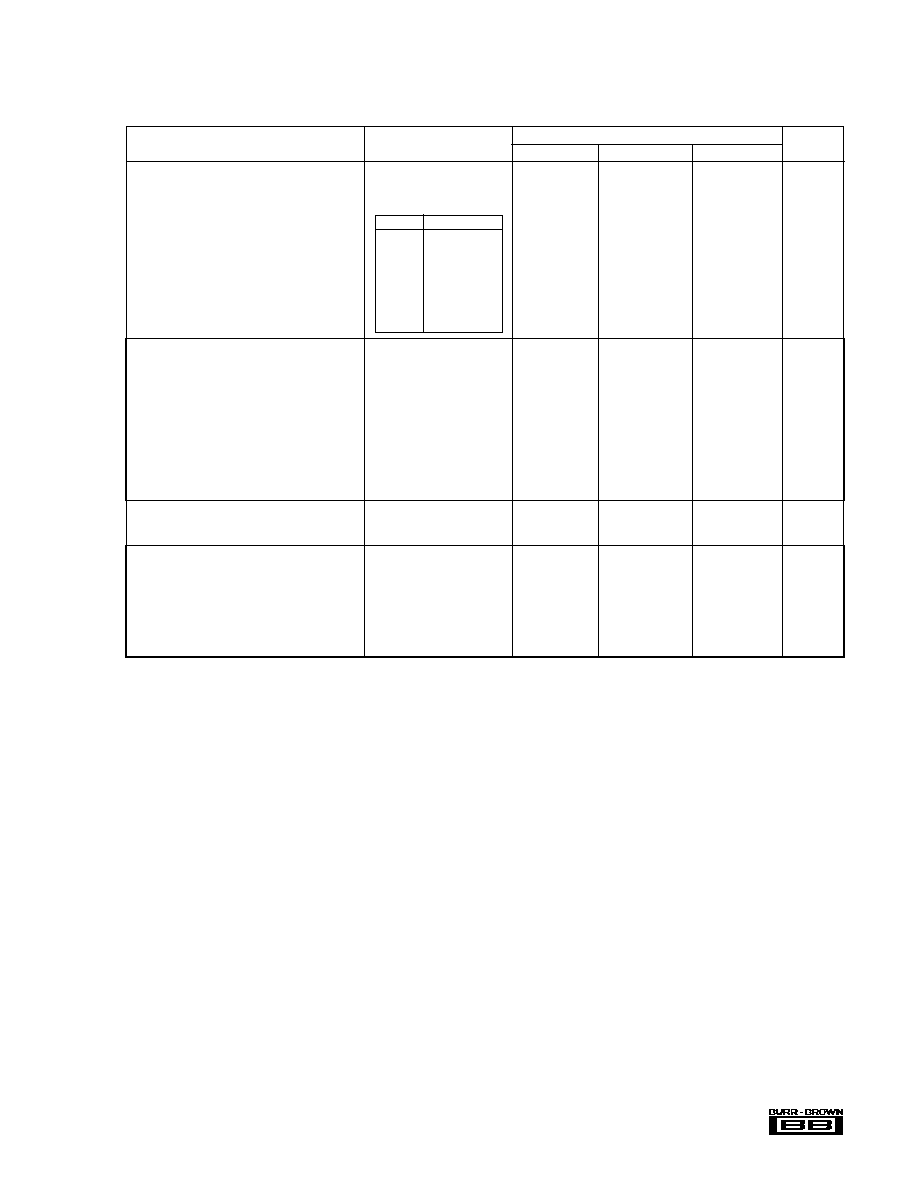
TRUTH TABLE
RS-485
DE
RE
BUS
0
0
R
X
0
1
HIGH Z
1
0
HIGH Z
1
1
T
X
FEATURES
q
RS-485 AND RS-422 COMPATIBLE
q
100% TESTED FOR HIGH-VOLTAGE
BREAKDOWN
q
RATED 1500Vrms
q
SINGLE-WIDE 24-PIN PLASTIC DIP
q
EASY TO USE
q
LOW POWER: 180mW typ at 5Mbit/s
APPLICATIONS
q
MULTIPOINT DATA TRANSMISSION
ON LONG BUS LINES IN NOISY
ENVIRONMENTS
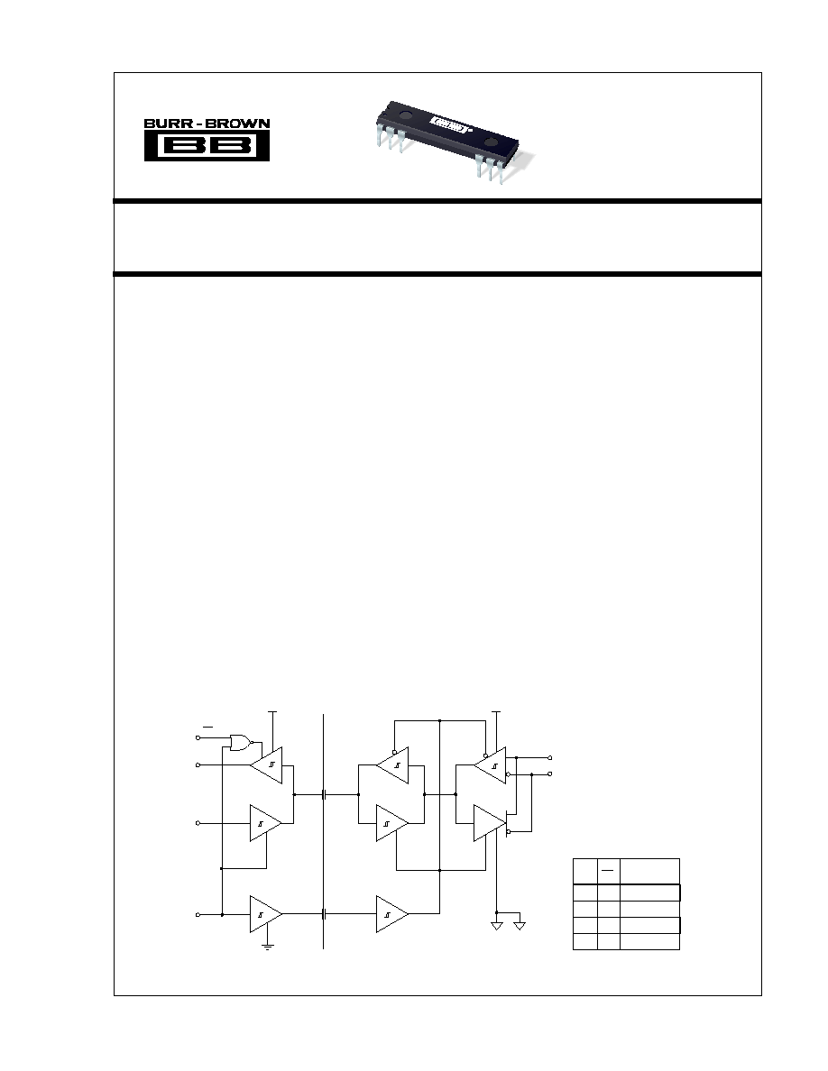
DESCRIPTION
The ISO485 differential, isolated bus transceiver uses
Burr-Brown's capacitively coupled isolation technol-
ogy to provide high-speed, low cost bus isolation.
The ISO485 is designed for bi-directional data com-
munication on multipoint bus transmission lines and
meets EIA Standard RS-485 as well as EIA Standard
RS-422A requirements.
The ISO485 uses high voltage 0.4pF capacitors in-
stead of the LED and photodetector which are used in
equivalent optocoupler solutions. As a consequence
the part count of the isolated RS-485 channel is
reduced from multiple optocoupler channels, an RS-
485 transceiver chip and supporting circuitry to one
ISO485. The capacitors in the ISO485 provide a high
voltage barrier, 1500Vrms and greatly reduce current
spikes on the power line.
The ISO485 combines a 3-state differential line driver
and a differential-input line receiver both of which
operate from a single 5V power supply. The driver
differential outputs and the receiver differential input/
output bus ports are designed to offer minimum load-
ing to the bus whenever the driver is disabled or
V
S
= 0V.
RE
A
B
D
R
DE
V
SA
22
23
24
11
14
3
2
1
V
SB
15
12
13
GND
B
GND
A
®
©1994 Burr-Brown Corporation
PDS-1280C
Printed in U.S.A. May, 1995

2
®
ISO485
SPECIFICATIONS
At T
A
= +25
°
C, V
S
= 5V, unless otherwise specified.
PARAMETER
CONDITION
MIN
TYP
MAX
UNITS
DRIVER DC CHARACTERISTICS
Input Voltage
High MIN
2
V
Low MAX
0.8
V
Input Current
High-Level
V
IN
= 2.4V
±
1
µ
A
Low-Level
V
IN
= 0.4V
±
1
µ
A
Output Voltage
I
OUT
= 0
0
5
V
Differential Output Voltage
I
OA
I
OB
= 0
1.5
5
V
R
LOAD
= 100
2
2.5
5
V
R
LOAD
= 54
1.5
2.5
5
V
Change In Magnitude of Differential
Output Voltage
R
LOAD
= 54
or 100
±
0.5
V
Common-Mode Output Voltage
R
LOAD
= 54
or 100
3
V
Change in Magnitude of Common-Mode
Output Voltage
R
LOAD
= 54
or 100
±
0.2
V
Output Current
V
OUT
= 7V, output disabled
1
mA
V
OUT
= 7V, output disabled
0.8
mA
Short-Circuit Output Current (1 sec max)
V
OUT
= 7V
250
mA
V
OUT
= 0V
150
mA
V
OUT
= V
S
250
mA
V
OUT
= 12V
250
mA
DRIVER SWITCHING CHARACTERISTICS
Propagation Delay Time,
Low-to-High Level Output
R
LOAD
= 54
60
ns
Propagation Delay Time,
High-to-Low Level Output
R
LOAD
= 54
60
ns
Input to Output Propagation Delay Skew
R
LOAD
= 54
10
ns
Output Rise Time
R
LOAD
= 54
10
ns
Output Fall Time
R
LOAD
= 54
10
ns
RECEIVER DC CHARACTERISTICS
Differential-Input-Threshold Voltage
High
V
OUT
= 2.7V, I
OUT
= 0.4mA
0.2
V
Low
V
OUT
= 0.5V, I
OUT
= 8mA
0.2
V
Hysteresis
70
mV
High-Level Output Voltage
V
ID
= 200mV, I
OH
= 400
µ
A
2.4
V
Low-Level Output Voltage
V
ID
= 200mV, I
OL
= 8mA
0.4
V
High-Impedance-State Output Current
V
OUT
= 1.4V
±
1
µ
A
Line Input Current
V
IN
= 12V, other output = 0V
0.7
mA
V
IN
= 7V, other output = 0V
0.6
mA
Enable-Input Current
High
V
IH
= 2.7V
1
µ
A
Low
V
IL
= 0.4V
1
µ
A
Input Resistance
12
k
Short-Circuit Output Current
1 sec max
40
mA
RECEIVER SWITCHING CHARACTERISTICS
Propagation Delay Time,
Low-to-High Level Output
V
ID
= 1.5V to 1.5V, C
L
= 15pF
35
60
ns
High-to-Low Level Output
V
ID
= 1.5V to 1.5V, C
L
= 15pF
30
60
ns
Input to Output Propagation Delay Skew
10
ns
Output Rise Time
R
L
= 54
8
ns
Output Fall Time
R
L
= 54
8
ns
TRANSCEIVER SPECIFICATIONS
Maximum Data Rate
20
35
Mbits/s
Propagation Delay Driver to Receiver
75
ns
Driver Output Enable Time
R
L
= 110
155
200
ns
Driver Output Disable Time
R
L
= 110
185
280
ns
Propagation Delay Receiver to Driver
13
ns
Receiver Output Enable Time
C
L
= 15pF
110
180
ns
Receiver Output Disable Time
C
L
= 15pF
120
185
ns
ISO485P
3
®
ISO485
SPECIFICATIONS
(CONT)
At T
A
= +25
°
C, V
S
= 5V, unless otherwise specified.
PARAMETER
CONDITION
MIN
TYP
MAX
UNITS
TRANSCEIVER SPECIFICATIONS (CONT)
Supply Voltage
V
S
A
3
5
5.5
V
V
S
B
4.75
5
5.25
V
Supply Current
DE RE
RS-485 BUS
V
S
A
0
0
Rx
5
mA
V
S
A
0
1
HIGH Z
0.4
mA
V
S
A
1
0
HIGH Z
0.4
mA
V
S
A
1
1
Tx
0.4
mA
V
S
B
0
0
Rx
55
mA
V
S
B
0
1
HIGH Z
55
mA
V
S
B
1
0
HIGH Z
51
mA
V
S
B
1
1
Tx
51
mA
RECOMMENDED OPERATING
CONDITIONS
Voltage at Any Bus Terminal
(separately or common-mode)
7
12
V
High-Level Driver Input Voltage
2
V
Low-Level Driver Input Voltage
0.8
V
Differential Receiver Input Voltage
±
12
V
Output Current High-Level
Driver
60
mA
Receiver
400
µ
A
Output Current Low-Level
Driver
60
mA
Receiver
8
mA
TEMPERATURE RANGE
Operating
40
85
°
C
Storage
40
125
°
C
ISOLATION PARAMETERS
Rated Voltage, Continuous
50Hz
1500
Vrms
Partial Discharge, 100% Test
(1)
1s, 5pC
2400
Vrms
Creepage Distance (External) DIP = "P" Package
16
mm
Internal Isolation Distance
0.10
mm
Isolation Voltage Transient Immunity
(2)
1.6
kV/
µ
s
Barrier Impedance
> 10
14
|| 7
|| pF
Leakage Current
240Vrms, 60Hz
0.6
µ
Arms
ISO485P
NOTES: (1) All devices receive a 1s test. Failure criterion is
5 pulses of
5pC. (2) The voltage rate-of-change across the isolation barrier that can be sustained
without data errors.
The information provided herein is believed to be reliable; however, BURR-BROWN assumes no responsibility for inaccuracies or omissions. BURR-BROWN assumes
no responsibility for the use of this information, and all use of such information shall be entirely at the user's own risk. Prices and specifications are subject to change
without notice. No patent rights or licenses to any of the circuits described herein are implied or granted to any third party. BURR-BROWN does not authorize or warrant
any BURR-BROWN product for use in life support devices and/or systems.
4
®
ISO485
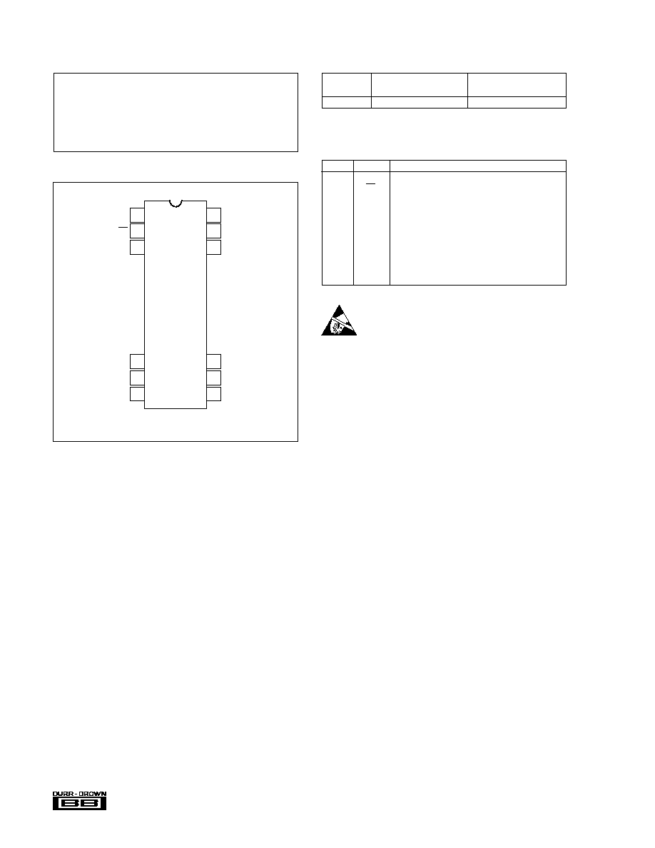
PIN #
NAME
DESCRIPTION
1
R
Data Received From Transmission Line
2
RE
Receive Switch Controlling Receiving Of Data
3
V
SA
+5V Supply Pin For Side A
10
NC
This Pin MUST Be Left Unconnected
11
GND
B
Ground Pin For Side B. Also Connected To Pin 14
12
A
Data, Driver Out/Receiver In
13
B
Data, Driver Out/Receiver In
14
GND
B
Ground Pin For Side B. Also Connected To Pin 11
15
V
SB
+5V Supply Pin For Side B
22
GND
A
Ground Pin For Side A
23
DE
Driver Switch Controlling Output Of Data
24
D
Data To Be Transmitted
Top View
DIP
ABSOLUTE MAXIMUM RATINGS
Supply Voltages, V
S
.............................................................................. 5.5V
Voltage at any bus terminal ......................................................... 10 to 15V
Enable Input Voltage ............................................................ 0 to V
CC
+ 0.5V
Continuous total dissipation at 25
°
C free-air temp. .......................... 750mW
Lead solder temperature, 260
°
C for 10s,
1.6mm below seating plane ............................................................... 300
°
C
Junction Temperature .......................................................................... 150
°
C
Package thermal transfer,
JA
........................................................... 75
°
C/W
PIN CONFIGURATION
NOTE: (1) Pin 10 must be left unconnected.
PACKAGE INFORMATION
PACKAGE DRAWING
MODEL
PACKAGE
NUMBER
(1)
ISO485P
24-Pin Single-Wide DIP
243-1
NOTE: (1) For detailed drawing and dimension table, please see end of data
sheet, or Appendix D of Burr-Brown IC Data Book.
PIN ASSIGNMENTS
24
23
22
15
14
13
1
2
3
10
11
12
R
RE
V
SA
NC
(1)
GND
B
A
D
DE
GND
A
V
SB
GND
B
B
ELECTROSTATIC
DISCHARGE SENSITIVITY
This integrated circuit can be damaged by ESD. Burr-Brown
recommends that all integrated circuits be handled with ap-
propriate precautions. Failure to observe proper handling and
installation procedures can cause damage.
ESD damage can range from subtle performance degradation
to complete device failure. Precision integrated circuits may
be more susceptible to damage because very small parametric
changes could cause the device not to meet its published
specifications.
5
®
ISO485
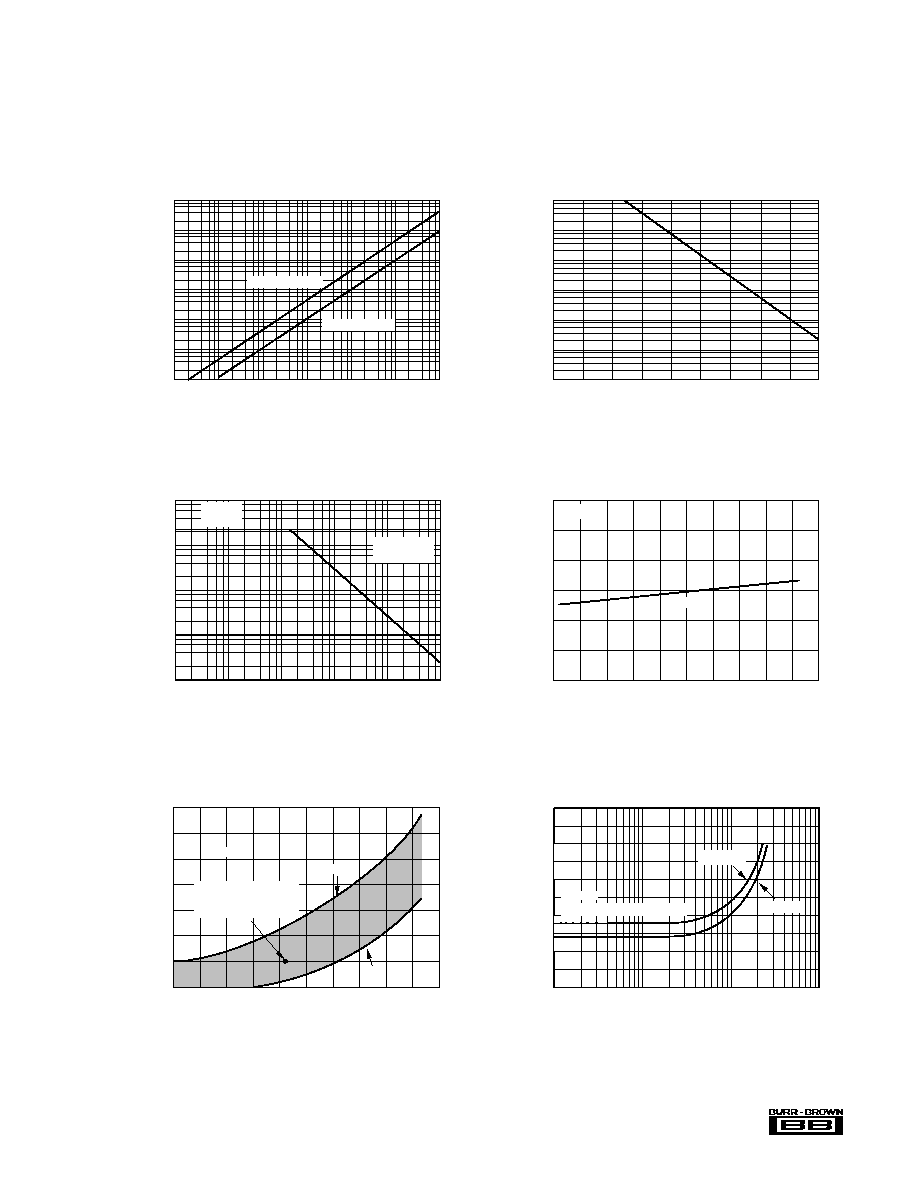
TYPICAL POWER DISSIPATION vs DATA RATE
500
400
300
200
100
0
100k
1M
10M
100M
Data Rate (Mbit/s)
Total Power (mW)
Transmit
Receive
NOTE:
Baud Rate = 2 · Frequency
NORMALIZED RISE/FALL TIME vs TEMPERATURE
1.6
1.5
1.4
1.3
1.2
1.1
1.0
0.9
60
40
20
0
20
40
60
80
100
120
140
Temperature (°C)
Relative t
r
, t
f
C
L
= 50pF
Normalized to Average
of Many Devices
at 25°C
+1
1
PROPAGATION DELAY vs TEMPERATURE
60
50
40
30
20
10
0
60
40
20
0
20
40
60
80
100 120
140
Temperature (°C)
Propagation Delay, t
PD
(ns)
V
S
= 5.0V
C
L
= 50pF
ISOLATION VOLTAGE vs FREQUENCY
10k
2.1k
1k
100
10
1
1k
10k
100k
1M
10M
100M
Frequency (Hz)
Peak Isolation Voltage (V)
Max DC
Rating
Degraded
Performance
TYPICAL INSULATION RESISTANCE vs TEMPERATURE
10
16
10
15
10
14
10
13
10
12
10
11
10
10
0
20
40
60
80
100
120
140
160
180
Temperature (°C)
Isolation Resistance (
)
ISOLATION LEAKAGE CURRENT vs FREQUENCY
100m
10m
1m
100µ
10µ
1µ
100n
1
10
100
1k
10k
100k
1M
Frequency (Hz)
Leakage Current (Arms)
V
ISO
= 240Vrms
V
ISO
= 1500Vrms
TYPICAL PERFORMANCE CURVES
At T
A
= +25
°
C, V
S
= +5V, unless otherwise noted.