ISO422
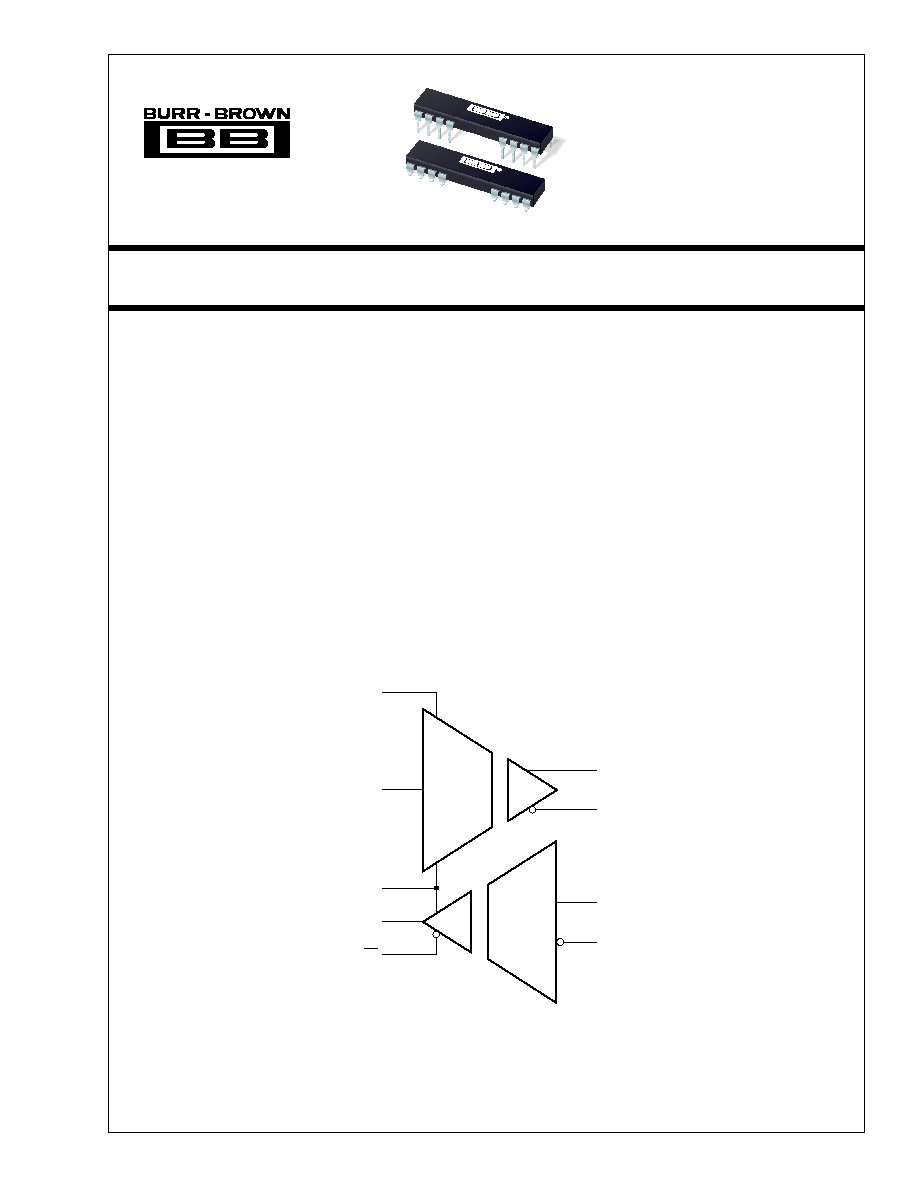
DIFFERENTIAL BUS TRANSCEIVER
FEATURES
q
FULL-/HALF-DUPLEX OPERATION
q
1500Vrms ISOLATION (cont)
q
2500Vrms ISOLATION (1 min)
q
2.5Mbps PERFORMANCE
q
LOOP-TEST FACILITY
APPLICATIONS
q
BUS TRANSMISSION SYSTEMS
q
GROUND LOOP ISOLATION
ISO422
®
©
1998 Burr-Brown Corporation
PDS-1503A
Printed in U.S.A. December, 1998
DESCRIPTION
ISO422 provides 1500Vrms isolation for industrial
bus transmission systems. ISO422 may be configured
in full or half duplex modes providing the user with
best flexibility for the application. Transmission rates
of 2.5Mbps can be obtained covering most require-
ments. A loop-back test facility is included. LBE
allows data on the D input to be routed to the R output
for test purposes.
ISO422 is available in 24-pin PDIP and 24-pin Gull
Wing
(1)
packages and is specified over the temperature
range 40
°
C to +85
°
C.
International Airport Industrial Park · Mailing Address: PO Box 11400, Tucson, AZ 85734 · Street Address: 6730 S. Tucson Blvd., Tucson, AZ 85706 · Tel: (520) 746-1111
Twx: 910-952-1111 · Internet: http://www.burr-brown.com/ · Cable: BBRCORP · Telex: 066-6491 · FAX: (520) 889-1510 · Immediate Product Info: (800) 548-6132
ISO422
ISO422
D
LBE
R
DE
Y
Z
A
B
RE
NOTE: (1) Gull Wing version available Q1'99.
2
®
ISO422
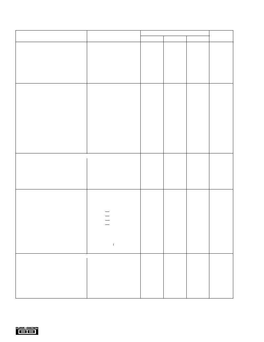
SPECIFICATIONS
At T
A
= +25
°
C, and V
S
= +5V, unless otherwise noted.
ISO422P, P-U
(1)
PARAMETER
CONDITIONS
MIN
TYP
MAX
UNITS
ISOLATION
Rated Continuous Isolation
V
ISO
50Hz, 60Hz
1500
V
Partial Discharge Voltage
1s, 5 x 5pC/per cycle
(2)
2500
V
Barrier Impedance
> 10
14
|| 10
|| pF
Leakage Current
240V, 60Hz
1
µ
A
2500V, 50Hz
10
µ
A
Creepage Distance
8.6
mm
Internal Isolation Distance
0.1
mm
Transient Recovery Time
5kV/
µ
s Edge
1
µ
s
DRIVER DC CHARACTERISTICS
High Level Input Voltage
V
IH
D and DE Inputs
(3)
2
V
Low Level Input Voltage
V
IL
D and DE Inputs
(3)
0.8
V
Input Leakage Current
I
L
D and DE Inputs
(3)
5
nA
Input Capacitance
C
IN
D and DE Inputs
(3)
5
pF
Output Voltage
V
O
V
Y
or V
Z
0
5
V
Differential Output Voltage
V
OD
I
OY
or I
OZ
= 0
1.5
5
V
R
L
= 100
2
3.6
5
V
R
L
= 54
1.5
2.8
5
V
Change in Mag Diff Out Voltage
|V
OD
|
R
L
= 100
or 54
(4)
±
40
±
200
mV
Common-Mode Output Voltage
V
OC
R
L
= 100
or 54
3
V
Change in Mag CM Out Voltage
|V
OC
|
R
L
= 100
or 54
(4)
±
40
±
200
mV
Output Current
I
O
V
O
= V
CC2
, Output Disabled
±
10
±
1000
nA
V
O
= 0V, Output Disabled
±
10
±
1000
nA
Short-Circuit Output Current
V
O
= V
CC2
, Continuous
100
mA
V
O
= 0V, Continuous
110
mA
DRIVER SWITCHING CHARACTERISTICS (Figure 6)
Differential Output Delay Time
t
DD
R
L
= 54
120
150
ns
Skew |t
DDH
- t
DDL
|
R
L
= 54
25
50
ns
Differential Output Transition Time
t
DT
R
L
= 54
100
ns
Output Enable Time to HIGH
t
DZH
R
L
= 100
120
150
ns
Output Enable Time to LOW
t
DZL
R
L
= 100
120
150
ns
Output Disable Time from HIGH
t
DHZ
R
L
= 100
120
150
ns
Output Disable Time from LOW
t
DLZ
R
L
= 100
120
150
ns
RECEIVER DC CHARACTERISTICS
High Level Output Voltage
V
OH
I
OH
= 6mA
V
CC
1
V
Low Level Output Voltage
V
OL
I
OL
= 6mA
0.4
V
Output Short-Circuit Current
I
OS
1s max
30
mA
Output HI-Z Leakage
I
OZ
V
OUT
= 0V
to V
CC1
±
10
±
1000
nA
Enable Input HIGH Threshold
V
IH
RE Input
(3)
2
V
Enable Input LOW Threshold
V
IL
RE Input
(3)
0.8
V
Input Leakage Current
I
L
RE Input
(3)
5
nA
Input Capacitance
C
IN
RE Input
(3)
5
pF
Differential Input HIGH Threshold
V
TH
V
O
= 2.8V
100
200
mV
Differential Input LOW Threshold
V
TL
V
O
= 0.4V
200
100
mV
Input Hysteresis
See Note 5
60
mV
Line Input Current
I
BI
Power On (GND
B
< V
BI
< V
SB
)
±
10
±
1000
nA
Line Voltage
V
BI
Power Off (I
BI
±
10mA max)
±
12
V
Input Resistance
R
IN
1
M
RECEIVER SWITCHING CHARACTERISTICS (Figure 7)
Propagation Delay L to H
t
RLH
V
ID
= 1.5V
to 1.5V, C
L
= 10pF
120
150
ns
Propagation Delay H to L
t
RHL
V
ID
= 1.5V
to 1.5V, C
L
= 10pF
120
150
ns
Skew |t
RLH
- t
RHL
|
40
ns
Output Rise Time
t
R
C
L
= 10pF
10
ns
Output Fall Time
t
F
C
L
= 10pF
10
ns
Output Enable Time to HIGH
t
RZH
C
L
= 10pF
15
25
ns
Output Enable Time to LOW
t
RZL
C
L
= 10pF
15
25
ns
Output Disable Time from HIGH
t
RHZ
C
L
= 10pF
15
25
ns
Output Disable Time from LOW
t
RLZ
C
L
= 10pF
15
25
ns
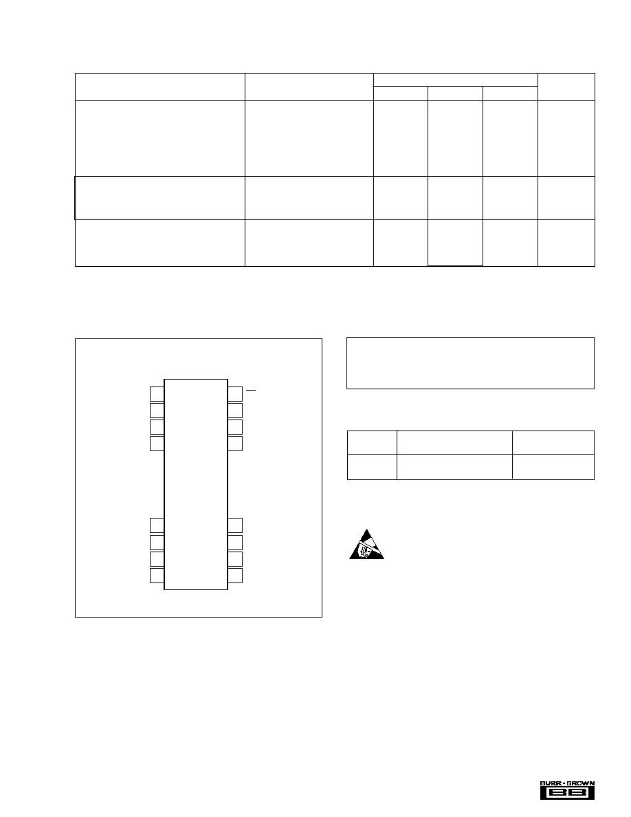
3
®
ISO422
POWER
Supply Voltage--Data Side
V
SA
4.5
5.5
V
Supply Current--Data Side
I
SA
Output Unloaded, dc
10
13
mA
Supply Current--Data Side
I
SA
Output Unloaded, max Rate
20
mA
Supply Voltage--Bus Side
V
SB
4.5
5.5
V
Supply Voltage--Bus Side
I
SB
Output Unloaded, dc
12
20
mA
Output Unloaded, max Rate
20
mA
BUS LIMITS
Input Current
±
10
mA
Maximum Differential Input
±
5
V
Maximum Data Rate
2.5
Mbps
TEMPERATURE RANGE
Operating
40
+85
°
C
Storage
40
+125
°
C
Thermal Resistance
JA
75
°
C/W
NOTES: (1) Gull Wing version available Q1'99. (2) All devices receive a 1s test. Failure criterion is > 5 pulses of > 5pC per cycle. (3) Logic inputs are HCT-type
and thresholds are a function of power supply voltage with approximately 100mV hysteresis. (4) Change in magnitude when the input is changed from HIGH to
LOW. (5) The difference between the differential low to high and high to low transition points.
The information provided herein is believed to be reliable; however, BURR-BROWN assumes no responsibility for inaccuracies or omissions. BURR-BROWN
assumes no responsibility for the use of this information, and all use of such information shall be entirely at the user's own risk. Prices and specifications are subject
to change without notice. No patent rights or licenses to any of the circuits described herein are implied or granted to any third party. BURR-BROWN does not
authorize or warrant any BURR-BROWN product for use in life support devices and/or systems.
SPECIFICATIONS
(CONT)
At T
A
= +25
°
C, and V
S
= +5V, unless otherwise noted.
ISO422P, P-U
(1)
PARAMETER
CONDITIONS
MIN
TYP
MAX
UNITS
PACKAGE DRAWING
PRODUCT
PACKAGE
NUMBER
(1)
ISO422P
24-Pin Plastic DIP
243-4
ISO422P-U
24-Pin Gull Wing Surface Mount
243-5
NOTE: (1) For detailed drawing and dimension table, please see end of data
sheet, or Appendix C of Burr-Brown IC Data Book.
PIN CONFIGURATION
Top View
DIP
ABSOLUTE MAXIMUM RATINGS
Supply Voltage: V
SA
............................................................. 0.5V to +6V
V
SB
............................................................. 0.5V to +6V
Continuous Isolation Voltage ..................................................... 1500Vrms
Storage Temperature ...................................................... 40
°
C to +125
°
C
Lead Temperature (soldering, 10s) ............................................... +300
°
C
PACKAGE INFORMATION
ELECTROSTATIC
DISCHARGE SENSITIVITY
Electrostatic discharge can cause damage ranging from per-
formance degradation to complete device failure. Burr-
Brown Corporation recommends that all integrated circuits
be handled and stored using appropriate ESD protection
methods.
ESD damage can range from subtle performance degrada-
tion to complete device failure. Precision integrated circuits
may be more susceptible to damage because very small
parametric changes could cause the device not to meet
published specifications.
24
23
22
21
16
15
14
13
1
2
3
4
9
10
11
12
DE
D
NC
V
SA
GND
B
GND
B
Y
Z
RE
R
LBE
GND
A
V
SB
V
SB
A
B
4
®
ISO422
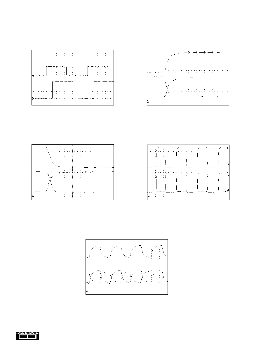
TYPICAL PERFORMANCE CURVES
At T
A
= +25
°
C, and V
S
= +5V, unless otherwise noted.
2
µ
s/div
BUS 0 TO 1 TRANSITION
BUS 1 TO 0 TRANSITION
TERMINATED 200m CABLE
2k
RESISTORS INSERTED IN TERMINATED CABLE
PROPAGATION DELAY
20ns/div
20ns/div
50ns/div
200ns/div
Y-Z
D
Y-Z
Z
Y
Y-Z
Y
Z
Y
Z
Y-Z
Y-Z
Y
Z
5
®
ISO422
OPERATION
ISO422 is an isolated, full-duplex bus transceiver which is
compatible with three-wire data bus systems using EIA
standards RS-422-A and RS-485. It is based on Burr-Brown's
capacitive barrier technology. The data bus input is designed
to present a very high impedance to the data bus, thus
allowing a virtually unlimited number of receivers on any
data bus section. To allow this feature, the data bus input is
limited to a common-mode range within the magnitude of
the supplies. This limitation requires that all nodes on the
bus are referenced to a common ground. However, systems
attached to the bus through ISO422, are isolated up to
1500Vrms and may, therefore, have local floating ground
potentials up to this isolation voltage. The circuit encodes all
data passed across the barrier to ensure that the input values
and control signals are correctly passed across the barrier
under all power up conditions. The ISO422 also allows data
recovery to the current input state, after any transient upset.
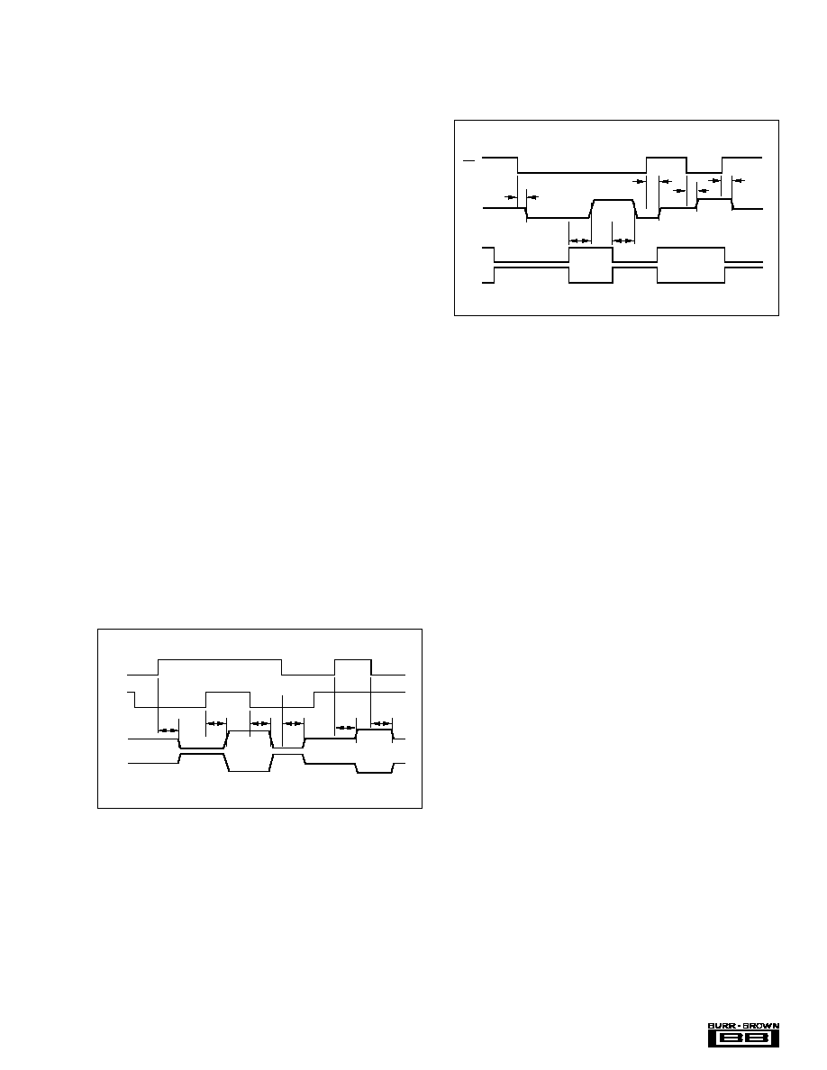
TRANSMIT
Data is passed from the D input to the data bus outputs after
a barrier transmission delay (t
DD
) when the DE input is
HIGH. When DE is LOW, the data bus drivers are switched
off, and assume the high impedance state. When enabling
the data bus output, i.e., switching DE from LOW to HIGH,
the enable signal is passed directly across the barrier and
enables the output, after a barrier transmission delay and
output enable time (t
DLZ
/t
DHZ
). Similarly, when disabling the
data bus output, i.e., switching DE from HIGH to LOW, the
disable signal is passed directly across the barrier and
disables the output after a barrier transmission delay and
output disable time (t
DLZ
/t
DHZ
).
active. The receive enable/disable time is simply the time to
enable/disable the R output (t
RLZ
) and does not require any
additional barrier transmission time.
FIGURE 1. ISO422 Data Transmit.
FIGURE 2. ISO422 Data Receive.
DATA CORRUPTION
If, due to transient upset, the data passed across the barrier
is corrupted, the data will be restored within 100ns from the
end of the corrupting signal.
SYNCHRONIZATION
The data transmitted across the barrier is coded using an
internal clock. This clock also captures the incoming asyn-
chronous data and synchronizes it to the clock edges. This
will give rise to an rms propagation delay jitter of approxi-
mately 50ns.
LOOPBACK
A loopback function is provided by the LBE input. If this
input is HIGH, then enabling both the transmitter and the
receiver will cause the device to route the D input to the R
output, in addition to the data bus outputs. Data on the
incoming bus is ignored. This feature allows a simple con-
nection test to be performed during any application. When
LBE is LOW, transmit and receive will operate in the normal
full-duplex mode.
DATA BUS CONNECTION
ISO422 can be used in half duplex, or full duplex data
communication bus systems. It is capable of continuously
driving a 54
load, equivalent to a double-terminated trans-
mission line, at the fully specified data rate. When connect-
ing to the data bus, the voltage on the A and B input lines
must remain between V
SB
and GND
B
. This can be achieved
by using a common bus ground connection, such as GND
B
,
as shown in Figures 5 and 6.
For any system connected to the bus, the isolation provided
by ISO422 allows the independent local ground potential to
be as high as 1500Vrms with respect to the date bus ground
reference. This feature replaces the limited +12V to 7V
range of the RS-485 standard with the full-isolation voltage
capability of the ISO422.
RECIEVE
The receive data is determined by the data bus differential
signal after a barrier transmission delay (t
RZL
). When the
difference between the A input and the B input (A-B) is
greater than +200mV, the R output will be HIGH. If A-B is
more negative than 200mV, the R output is undefined.
Since the reciver has a high impedance input, no disable
signal is required for the data bus input, which is always
DE
D
Y
Z
t
DZL
t
DD
t
DLZ
t
DZH
t
DHZ
t
DD
t
RZL
t
RLZ
t
RZH
t
RZH
t
RLH
t
RHL
A
B
R
RE