
DSP101
DSP102
FEATURES
q
ZERO-CHIP INTERFACE TO STANDARD
DSP ICs: AD, AT&T, MOTOROLA, TI
q
SINGLE CHANNEL: DSP101
q
DUAL CHANNEL: DSP102
Two Serial Outputs or Cascade to Single
32-Bit Word
q
SAMPLING RATE TO 200kHz
q
DYNAMIC SPECIFICATIONS:
Signal/(Noise + Distortion) = 88dB;
Spurious-Free Dynamic Range = 94dB;
THD = 91dB
q
SERIAL OUTPUT DATA COMPATIBLE
WITH 16-, 24-, AND 32-BIT DSP IC
FORMATS
DESCRIPTION
The DSP101 and DSP102 are high performance sam-
pling analog-to-digital converters designed for sim-
plicity of use with modern digital signal processing
ICs. Both are complete with all interface logic for use
directly with DSP ICs, and provide full sampling and
conversion at rates up to 200kHz.
The DSP101 offers a single conversion channel, with
18 bits of serial data output, allowing the user to drive
16-bit, 24-bit, or 32-bit DSP ports. The DSP102 offers
two complete conversion channels, with either two
full 18-bit output ports, or a mode to cascade two
16-bit conversions into a 32-bit port as one word.
Both the DSP101 and DSP102 are packaged in stan-
dard, low-cost 28-pin plastic DIP packages. Each is
offered in two performance grades to match applica-
tion requirements.
18-Bit Sampling ADC
18-Bit Sampling ADC
Reference
Convert
Command
Analog
Input
Channel A
Analog
Input
Channel B
Channel B on DSP102 Only
Control
Logic
Select Sync Format
Channel A User Tag In
Sync
Bit Clock
Channel A Data/
Cascaded Data
Channel B Data
Channel B User Tag In
Cascade
International Airport Industrial Park · Mailing Address: PO Box 11400 · Tucson, AZ 85734 · Street Address: 6730 S. Tucson Blvd. · Tucson, AZ 85706
Tel: (520) 746-1111 · Twx: 910-952-1111 · Cable: BBRCORP · Telex: 066-6491 · FAX: (520) 889-1510 · Immediate Product Info: (800) 548-6132
®
DSP-Compatible Sampling Single/Dual
ANALOG-TO-DIGITAL CONVERTERS
©
1990 Burr-Brown Corporation
PDS-1068C
Printed in U.S.A. October. 1993
®
DSP101/102
2
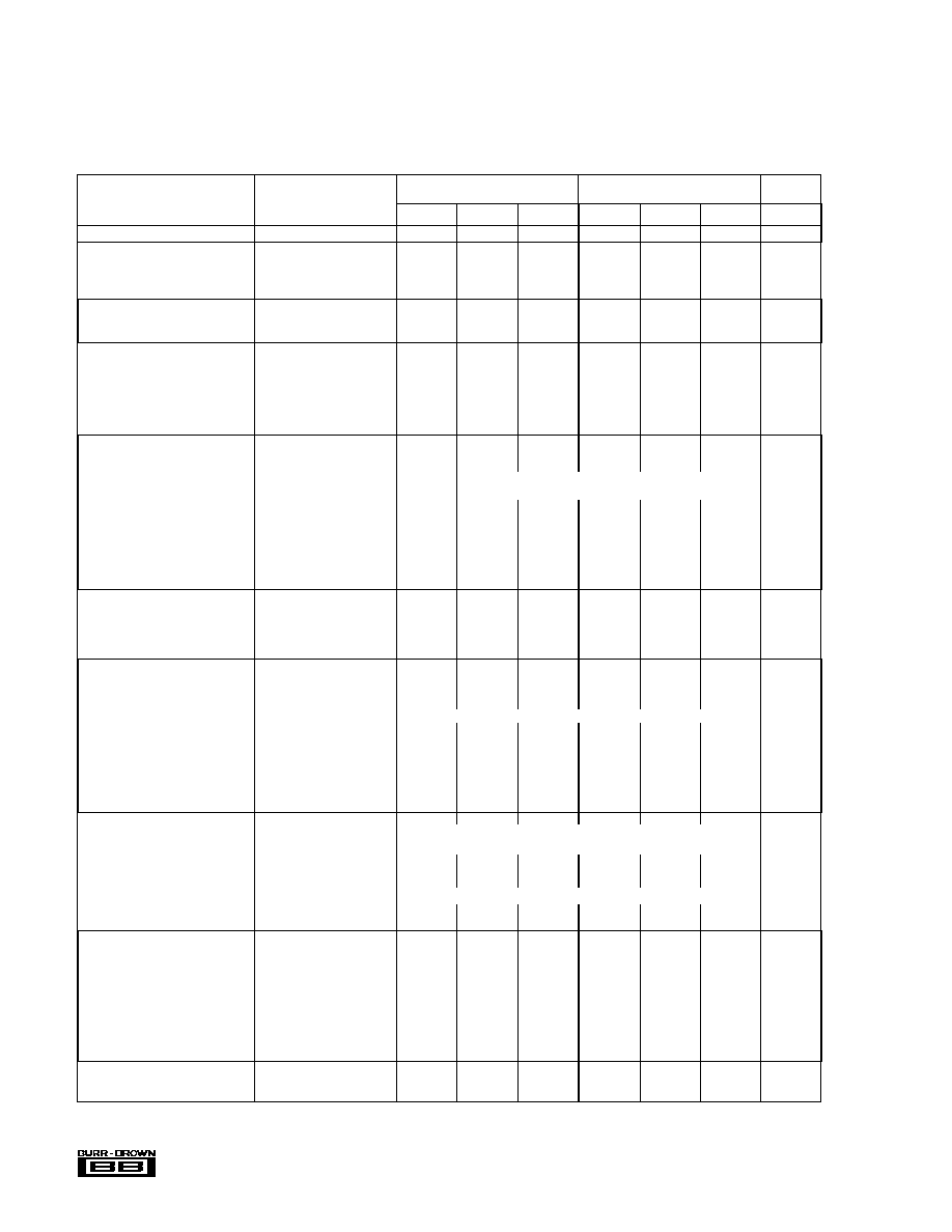
SPECIFICATIONS
ELECTRICAL
At T
A
= 0
°
C to 70
°
C,
±
2.75V input signal, sampling frequency (f
S
) = 200kHz, V
A
+ = V
D
= +5V, V
A
= 5V, 16MHz external clock on OSC1, CLKOUT tied to CLKIN,
8MHzdata transfer clock on XCLK, data analysis band-limited to 20kHz, unless otherwise specified.
Sufficient to meet AC Accuracy Specifications
Sufficient to meet AC Accuracy Specifications
DSP101JP
DSP101KP
DSP102JP
DSP102KP
PARAMETER
CONDITIONS
MIN
TYP
MAX
MIN
TYP
MAX
UNITS
RESOLUTION
18
*
Bits
ANALOG INPUT
Voltage Range
±
2.75V
*
V
Impedance
1
*
k
Capacitance
20
*
pF
THROUGHPUT SPEED
Complete Cycle
Acquisition + Conversion
5
*
µ
s
Throughput Rate
200
*
kHz
AC ACCURACY
(1)
Signal-to-(Noise + Distortion) Ratio
f
IN
= 1kHz
83
86
86
88
dB
(2)
f
IN
= 1kHz (60dB)
32
*
dB
f
IN
= 25kHz
82
*
dB
Total Harmonic Distortion
f
IN
= 1kHz
90
86
91
89
dB
Spurious-Free Dynamic Range
f
IN
= 1kHz
89
92
92
94
dB
Signal-to-Noise Ratio (SNR)
f
IN
= 1kHz
84
88
87
89
dB
DC ACCURACY
Gain Error
±
5
*
%
Gain Error Mismatch
DSP102 Channels
±
2
*
%
Integral Linearity
±
2.75V Input Range
Differential Linearity
±
2.75V Input Range
Integral Linearity Error
±
0.7V Input Range
±
0.003
*
%
Differential Linearity Error
±
0.7V Input Range
±
0.002
*
%
No Missing Codes
±
0.7V Input Range
14
*
Bits
Bipolar Zero Error
(3)
±
2
mV
Bipolar Zero Mismatch
(3)
DSP102 Channels
±
2
mV
Power Supply Sensitivity
5.25V < V
A
< 4.75V
60
*
dB
+4.75V < V
A
+, V
D
+ < +5.25V
60
*
dB
SAMPLING DYNAMICS
Aperture Delay
30
*
ns
Aperture Jitter
100
*
ps, rms
Transient Response
1
*
µ
s
Overvoltage Recovery
5
*
µ
s
DIGITAL INPUTS
Logic Levels (Except OSC1)
V
IL
I
L
=
±
10
µ
A
0
+0.8
*
*
V
V
IH
I
H
=
±
10
µ
A
+2.4
+5
*
*
V
OSC1 Clock
74HC Compatible
Frequency
16
MHz
Data Transfer Clock (XCLK)
Frequency
0.1
12
*
*
MHz
Duty Cycle
40
50
60
*
*
%
Conversion Clock (CLKIN)
Frequency
0.5
5.33
*
*
MHz
Duty Cycle
25
33
55
*
*
*
%
DIGITAL OUTPUTS
Format
Serial; MSB first; 16/18-bit and Cascaded 32-bit Mode
Coding
Binary Two's Complement
Logic Levels (Except OSC2)
V
OL
I
SINK
= 4mA
0
+0.4
*
*
V
V
OH
I
SOURCE
= 4mA
+2.4
+5
*
*
V
OSC2
Can only be used to drive crystal oscillator.
Conversion Clock (CLKOUT)
Drive Capability
±
2mA
*
mA
POWER SUPPLIES
Rated Voltage
V
A
+
+4.75
+5
+5.25
*
*
*
V
V
A
5.25
5
4.75
*
*
*
V
V
D
+4.75
+5
+5.25
*
*
*
V
Power Consumption
XCLK = OSC1 = 12MHz
250
425
*
*
mW
Supply Current
XCLK = OSC1 = 12MHz
I
A
+
30
45
*
*
mA
I
A
18
25
*
*
mA
I
D
5
15
*
*
mA
TEMPERATURE RANGE
Specification
0
+70
*
*
o
C
Storage
65
+125
*
*
o
C
NOTES: (1) All dynamic specifications are based on 2048-point FFTs, using four-term Blackman-Harris window. (2) All specifications in dB are referred to a full-
scale input,
±
2.75Vp-p. (3) Adjustable to zero with external potentiometer.

®
DSP101/102
3
DSP102 CHANNEL SEPARATION ON CHANNEL B WITH
±2.75V, 1kHz INPUT ON CHANNEL A
Frequency (kHz)
0
0
Magnitude (dB)
20
40
60
80
100
120
25
50
75
100
FREQUENCY SPECTRUM of ±2.75V, 451kHz INPUT
(Using Four-Term Blackman-Harris Window)
Frequency (kHz)
0
0
Magnitude (dB)
20
40
60
80
100
120
25
50
75
100
Undersampling
SINAD means Signal-to-(Noise + Distortion) Ratio.
THD means Total Harmonic Distortion thru 8th harmonic.
SNR means Signal-to-Noise Ratio excluding harmonics
SFDR means Spurious Free Dynamic Range, including
thru the 8th.
harmonics.
TYPICAL PERFORMANCE CURVES
At T
A
= +25
°
C, V
A
+ = V
D
+ = +5V, V
A
= V
D
= 5V, Sampling Frequency f
S
= 200kHz; External Clock Input at OSC1 = 80f
S
= 16MHz, XCLK = 40f
S
= 8MHz; Using
2048 Point FFT; Data analysis limited to 0 to 20kHz band; Unless otherwise specified.
55 40 25
0
25
70
85
125
Ambient Temperature (°C)
DYNAMIC PERFORMANCE vs TEMPERATURE
SINAD, SNR and SFDR (dB)
THD (dB)
80
85
90
95
80
85
90
95
100
100
f
IN
= 1kHz, ±2.75V
SINAD
THD
SNR
SFDR
FREQUENCY SPECTRUM of ±2.75V, 1kHz INPUT
(Average of 12 FFTs, No Window Used)
Frequency (kHz)
0
0
25
50
75
100
Magnitude (dB)
30
60
90
120
FREQUENCY SPECTRUM of ±2.75V, 20kHz INPUT
(Using Four-Term Blackman-Harris Window)
Frequency (kHz)
0
0
Magnitude (dB)
20
40
60
80
100
120
25
50
75
100
INTERMODULATION DISTORTION WITH 1kHz AND 3kHz INPUTS
(Using Four-Term Blackman-Harris Window)
Frequency (kHz)
0
0
Magnitude (dB)
20
40
60
80
100
120
25
50
75
100

®
DSP101/102
4
55 40 25
0
25
70
85
125
Ambient Temperature (°C)
DYNAMIC PERFORMANCE vs TEMPERATURE
(Data Analysis Over Full 0 to 100kHz Band)
SINAD, SNR and SFDR (dB)
THD (dB)
75
80
85
90
95
75
80
85
90
95
100
100
f
IN
= 1kHz, ±2.75V
SINAD
THD
SFDR
SNR
TYPICAL PERFORMANCE CURVES
(CONT)
At T
A
= +25
°
C, V
A
+ = V
D
+ = +5V, V
A
= V
D
= 5V, Sampling Frequency f
S
= 200kHz; External Clock Input at OSC1 = 80f
S
= 16MHz, XCLK = 40f
S
= 8MHz; Using
2048 Point FFT; Data analysis limited to 0 to 20kHz band; Unless otherwise specified.
000E
Output Code and Equivalent Voltage
(Binned at 16-bit level)
HISTOGRAM OF 5k CONVERSION RESULTS ON DSP102
(Both Inputs Grounded)
Number of Conversions Yielding This Code
2500
2000
1500
1000
500
0
Channel A
Channel B
1.17mV
0000
0V
FFF7
FFF1
1.26mV
Code
Voltage
70
75
80
85
90
95
70
75
80
85
90
95
100
100
30
0
60
90
120
150
180
Conversion Rate (kHz)
SINAD, SNR and SFDR (dB)
THD (dB)
DYNAMIC PERFORMANCE vs CONVERSION RATE
(Data Analysis over Full 0 to f
S
/2 Band,
OSC1 = 12.288MHz, XCLK = 3.072MHz)
SINAD
SNR
THD
SFDR
f
IN
= 1kHz, ±2.75V (0dB)
60
70
80
90
1
10
100
1000
Input Frequency (kHz)
Total Harmonic Distortion (dB)
TOTAL HARMONIC DISTORTION
vs INPUT FREQUENCY
100
±2.75V Input (0dB)
55 40 25
0
25
70
85
125
Ambient Temperature (°C)
DYNAMIC PERFORMANCE vs TEMPERATURE
(f
S
= 180kHz Asychronous to 12.288MHz
Crystal Between OSC1 and OSC2)
SINAD, SNR and SFDR (dB)
THD (dB)
70
75
80
85
90
95
70
75
80
85
90
95
100
100
Ambient Temperature (°C)
f
IN
= 1kHz, ±2.75V
THD
SFDR
SNR
SINAD
100
90
80
70
60
50
40
30
20
10
0.1
1
10
100
Input Frequency (kHz)
SINAD (dB)
SINAD vs INPUT FREQUENCY
(Data Analysis over Full 0 to 100kHz Band)
0
±2.75V Input (0dB)
±0.275V Input (20dB)
±2.75mV Input (60dB)

®
DSP101/102
5
TYPICAL DSP102 FFT SETUP
REF
VINB
VPOTB
Burr-Brown
ZPB34
DSP
Processor
CASC
SSF
OSC1
CLKOUT
CLKIN
CONV
XCLK
SYNC
SOUTA
DSP102
22
12
11
15
20
200kHz
150
16MHz TTL Oscillator
FFT
Software
÷80
÷2
+5V
10
13
21
16
8MHz
27
26
25
0.1µF
1
10µF
+
10µF
+
220pF
150
220pF
Brüel & Kjaer
Model 1049
Digital Signal
Generator
6 Pole,
150kHz
Low-Pass
Filter
1kHz
1/2
OPA2604
1/2
OPA2604
2
VPOTA
±2.75V
VINA
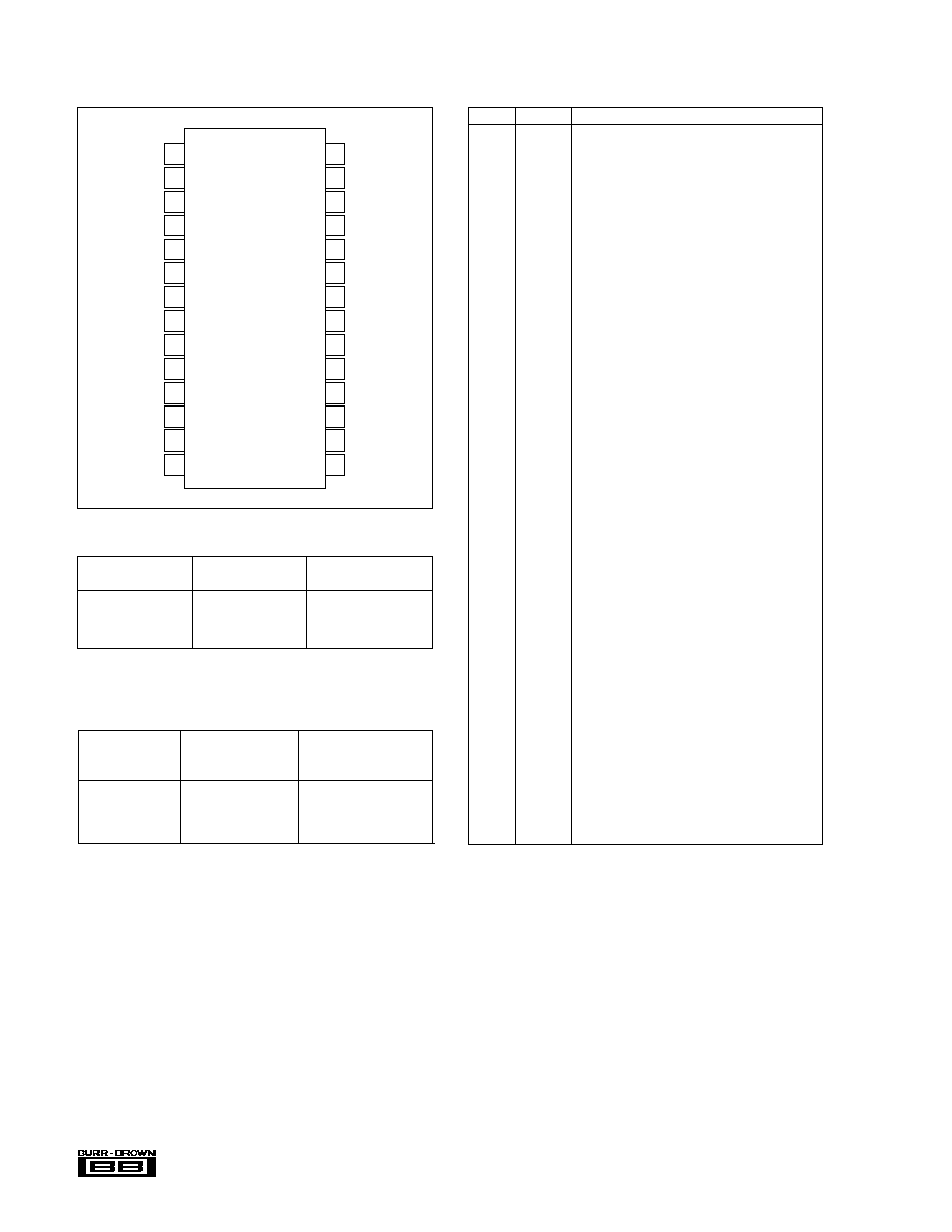
DSP101 PIN ASSIGNMENTS
PIN #
NAME
DESCRIPTION
1
VPOT
Trim Reference Out. 10
µ
F Tantalum to AGND.
Voltage on this pin is approximately 2.75V.
2
VIN
Analog In.
3
MSB
MSB Adjust In.
4
VOS
VOS Adjust In.
5
V
A
5V Analog Power.
6
V
A
+
+5V Analog Power.
7
DGND
Digital Ground.
8
DGND
Digital Ground.
9
V
D
+5V Digital Power.
10
CLKIN
Conversion Clock In.
11
CLKOUT
Conversion Clock Out. Can drive multiple
DSP101/DSP102s to synchronize conversion.
12
SSF
Select Synch Format In. If HIGH, SYNC will be
active High. If LOW, SYNC will be active Low.
See timing diagram (Figure 1).
13
OSC1
Oscillator Point 1 Input/External Clock In. If using
external clock, drive with 74HC logic levels.
Connect to DGND if not used.
14
OSC2
Oscillator Point 2 Output. Provides drive for
crystal oscillator. Make no electrical connection if
using external clock.
15
SYNC
Data Synchronization Out. Active High when SSF
is HIGH; active Low when SSF is LOW.
16
XCLK
Data Transfer Clock In.
17
No Internal Connection.
18
TAG
User Tag In. Data clocked into this pin is
appended to the conversion results on SOUT.
See timing diagram (Figure 1).
19
No Internal Connection.
20
SOUT
Serial Data Out. MSB first, Binary Two's
Complement format.
21
CONV
Convert Command In. Falling edge puts converter
into hold state, initiates conversion, and transmits
previous conversion results to DSP IC with
appropriate SYNC pulse.
22
DGND
Digital Ground.
23
No Internal Connection.
24
No Internal Connection.
25
No Internal Connection.
26
CAP
Bypass Capacitor. 10
µ
F Tantalum to AGND.
Voltage on this pin is approximately 2.7V.
27
REF
Reference Bypass. 0.1
µ
F Ceramic to AGND.
Voltage on this pin is approximately 3.8V.
28
AGND
Analog Ground.
DSP101 PIN CONFIGURATION
ABSOLUTE MAXIMUM RATINGS
V
A
+ to Analog Common .................................................................... +7V
V
A
to Analog Common .................................................................... 7V
V
D
to Digital Common ........................................................................ +7V
Analog Common to Digital Common ...................................................
±
1V
Control Inputs to Digital Common ............................... 0.5 to V
D
+ 0.5V
Analog Input Voltage ..........................................................................
±
5V
Maximum Junction Temperature .................................................... 150
o
C
Internal Power Dissipation ............................................................. 825mW
Lead Temperature (soldering, 10s) ............................................... +300
o
C
Thermal Resistance,
JA
, Plastic DIP ............................................ 50
o
C/W
1
2
3
4
5
6
7
8
9
10
11
12
13
14
28
27
26
25
24
23
22
21
20
19
18
17
16
15
VPOT
VIN
MSB
VOS
V
V +
DGND
DGND
V
D
CLKIN
CLKOUT
SSF
OSC1
OSC2
A
A
AGND
REF
CAP
DGND
CONV
SOUT
TAG
XCLK
SYNC
DSP101
Top View
DIP
®
DSP101/102
6
DSP102 PIN ASSIGNMENTS
PIN #
NAME
DESCRIPTION
1
VPOTA
Channel A Trim Reference Out. 10
µ
F Tantalum to
AGND. Voltage on this pin is approximately 2.75V.
2
VINA
Channel A Analog In.
3
MSBA
Channel A MSB Adjust In.
4
VOSA
Channel A VOS Adjust In.
5
V
A
5V Analog Power.
6
V
A
+
+5V Analog Power.
7
DGND
Digital Ground.
8
DGND
Digital Ground.
9
V
D
+5V Digital Power.
10
CLKIN
Conversion Clock In.
11
CLKOUT
Conversion Clock Out. Can drive multiple DSP101/
DSP102s to synchronize conversion.
12
SSF
Select Synch Format In. If HIGH, SYNC will be
active High. If LOW, SYNC will be active Low. See
timing diagram (Figure 1).
13
OSC1
Oscillator Point 1 Input / External Clock In. If using
external clock, drive with 74HC logic levels.
Connect to DGND if not used.
14
OSC2
Oscillator Point 2 Output. Provides drive for crystal
oscillator. Make no electrical connection if using
external clock.
15
SYNC
Data Synchronization Out. Active High when SSF
is HIGH; active Low when SSF is LOW.
16
XCLK
Data Transfer Clock In.
17
SOUTB
Channel B Serial Data Out. MSB first, Binary
Two's Complement format.
18
TAGA
Channel A User Tag In. Data clocked into this pin
is appended to the conversion results of SOUTA.
See timing diagram (Figure 1).
19
TAGB
Channel B User Tag In. Data clocked into this pin
is appended to the conversion results of SOUTB.
See timing diagram (Figure 1).
20
SOUTA
Channel A Serial Data Out. MSB first, Binary
Two's Complement format. If CASC is HIGH, 32
bits of data output, with first 16 bits being Channel
A data.
21
CONV
Convert Command In. Falling edge puts converter
into hold state, initiates conversion, and transmits
previous conversion results to DSP IC with
appropriate SYNC pulse.
22
CASC
Select Cascade Mode In. If HIGH, DSP102
transmits a 32-bit word on SOUTA, with the first 16
bits being data on Channel A. If LOW, DSP102
transmits data for both channels simultaneously.
23
VOSB
Channel B VOS Adjust In.
24
MSBB
Channel B MSB Adjust In.
25
VINB
Channel B Analog In.
26
VPOTB
Channel B Trim Reference Out. 10
µ
F Tantalum to
AGND. Voltage on this pin is approximately 2.75V.
27
REF
Reference Bypass. 0.1
µ
F Ceramic to AGND.
Voltage on this pin is approximately 3.8V.
28
AGND
Analog Ground.
DSP102 PIN CONFIGURATION
The information provided herein is believed to be reliable; however, BURR-BROWN assumes no responsibility for inaccuracies or omissions. BURR-BROWN assumes
no responsibility for the use of this information, and all use of such information shall be entirely at the user's own risk. Prices and specifications are subject to change
without notice. No patent rights or licenses to any of the circuits described herein are implied or granted to any third party. BURR-BROWN does not authorize or warrant
any BURR-BROWN product for use in life support devices and/or systems.
Top View
DIP
1
2
3
4
5
6
7
8
9
10
11
12
13
14
28
27
26
25
24
23
22
21
20
19
18
17
16
15
VPOTA
VINA
MSBA
VOSA
V
A
V
A
+
DGND
DGND
V
D
CLKIN
CLKOUT
SSF
OSC1
OSC2
AGND
REF
VPOTB
VINB
MSBB
VOSB
CASC
CONV
SOUTA
TAGB
TAGA
SOUTB
XCLK
SYNC
DSP102
ORDERING INFORMATION
NUMBER
SIGNAL-TO-
OF
(NOISE + DIST.) RATIO
MODEL
CHANNELS
dB min
DSP101JP
1
83
DSP101KP
1
86
DSP102JP
2
83
DSP102KP
2
86
PACKAGE INFORMATION
PACKAGE DRAWING
MODEL
PACKAGE
NUMBER
(1)
DSP101JP
28-Pin Plastic DIP
215
DSP101KP
28-Pin Plastic DIP
215
DSP102JP
28-Pin Plastic DIP
215
DSP102KP
28-Pin Plastic DIP
215
NOTE: (1) For detailed drawing and dimension table, please see end of data
sheet, or Appendix D of Burr-Brown IC Data Book.

®
DSP101/102
7
FIGURE 1. DSP101 and DSP102 Timing.
NOTES: (1) When using a DSP IC in a 16-bit mode, these data bits will be ignored by the processor. (2) f
OSC1
must be at least 72 times faster than the conversion rate. (t
3
, t
4
72 t
12
)
SYMBOL
DESCRIPTION (C
L
= 50pF)
MIN
MAX
UNITS
t
1
XCLK period. Duty Cycle 50%
±
10%
83
ns
t
2
Convert Command LOW Time
50
ns
t
3
Convert Period (CASC = LOW on DSP102)
24
t
1
t
4
Convert Period (CASC = HIGH on DSP102)
40
t
1
t
5
SYNC Active Delay after Convert Falling Edge
t
1
+40
2 t
1
ns
t
6
SYNC LOW to HIGH Delay from XCLK Rising
15
ns
t
7
SYNC HIGH to LOW Delay from XCLK Rising
15
ns
t
8
SOUTA/B Data Valid Delay from XCLK Rising
15
ns
t
9
SOUTA/B Data Valid After from XCLK Rising
10
ns
t
10
TAGA/B Data Setup before XCLK Rising
20
ns
t
11
TAGA/B Data Hold after XCLK Rising
0
n
s
t
12
OSC1 Period.
(2)
Duty Cycle 50%
±
10%
62
667
ns
t
13
CLKOUT Period. Duty Cycle 33%
±
1
0
%
3
t
12
ns
t
14
CLKIN Period. Duty Cycle 33%
±
20%
186
2000
ns
t
15
CLKIN HIGH
62
1050
t
16
CLKIN LOW
84
1340
t
12
t
13
t
14
OSC1
CLKOUT
CLKIN
Conversion Clock Timing
(2)
t
15
t
16
XCLK
CONV
SYNC (SSF = HIGH)
SYNC (SSF = LOW)
XCLK
CONV
SOUTA (CASC = HIGH)
Bit 1 (MSB)
t
2
t
5
t
3
t
2
t
6
t
7
t
6
t
7
t
4
t
9
Bit 1 (MSB)
Bit 2
Bit 16 (LSB)
t
2
t
1
t
1
t
2
Bit 16
DSP102 Cascade Mode (CASC = HIGH)
Channel A Data
Channel B Data
SOUTA/B (CASC = LOW on DSP102)
t
9
Bit 1 (MSB)
Bit 2
Bit 16
Bit 17
Bit 18 (LSB)
(1)
(2)
t
8
TAG Bit 1
TAG Bit 2
TAGA/B
t
11
TAG Bit 1
TAG Bit 2
t
10
t
8

®
DSP101/102
8
THEORY OF OPERATION
The DSP101 and DSP102 are sampling analog-to-digital
converters optimized for handling dynamic signals. They
have complete logic interface circuitry for ease of use with
standard digital signal processing ICs, and transmit data
words in a serial stream. The successive approximation
conversion architecture is combined with an inherently sam-
pling switched capacitor array to provide maximum user
flexibility over sampling and conversion timing.
The DSP101 and DSP102 are pipelined internally. When the
user gives a convert command at time (t), two actions are
initiated. First, the internal sample/holds are switched to the
hold state, and a conversion cycle is initiated. At the same
time, the DSP101 or DSP102 transmits a synchronization
pulse and starts shifting out the conversion results from the
previous convert command at (t-1) using the system bit
clock. The data from the conversion at time (t) is shifted out
of the converter after the next convert command is received.
Both the DSP101 and the DSP102 are 18-bit A/Ds inter-
nally. When the DSP IC is programmed to accept 16-bit
word lengths, the processor will ignore the last two data bits
transmitted from the DSP101 or DSP102. A Cascade Mode
on the DSP102 can be invoked to transmit data for both
conversion channels over a single serial line as a 32-bit
word. In this mode, the first 16 bits of data transmitted after
the Sync pulse contain data from channel A, followed by 16
bits of information from channel B, allowing a single 32-bit
word to contain data for both channels.
A unique Tag feature allows additional digital data to be
appended to the conversion results, so that a single data
word contains conversion results plus other signal informa-
tion, such as gain settings or multiplexer channel settings in
front of the converter.
The DSP101 and DSP102 are high-resolution A/D convert-
ers complete with sampling capability and on-board refer-
ences. They can acquire and convert analog signals at up to
a 200kHz sampling rate. Both operate from
±
5V supplies,
and have full-scale analog input ranges of
±
2.75V.
BASIC OPERATION
Figure 2 shows the minimum connections required to oper-
ate the DSP101. The falling edge of a convert command on
pin 21 puts the internal sampling capacitor array into the
hold state. The falling edge on pin 21 also starts the process
to initiate a conversion and transmit data from the previous
conversion, synchronizing both appropriately to the 10MHz
clock input on pin 13. Figure 1 shows the timing relationship
between the convert command, the output data, and the
synchronization pulse.
In this basic system, the 10MHz clock is used both to
generate a 3.33MHz conversion clock and as the data trans-
fer bit clock for outputting data. Per Figure 1, there must be
at least 72 clock pulses on pin 13 between convert com-
mands, so that this circuit can sample and convert at up to
138kHz.
FIGURE 2. DSP101 Basic Operation.
1
2
3
4
5
6
7
8
9
10
11
12
13
14
28
27
26
25
24
23
22
21
20
19
18
17
16
15
10µF
10µF
0.1µF
AGND
REF
CAP
NC
NC
NC
DGND
CONV
SOUT
NC
TAG
NC
XCLK
SYNC
DSP101
+
+
10µF
5V
+5V
NOTES: (1) Leave Unconnected.
(2) Protection from power supply momentary overrange.
VPOT
VIN
MSB
VOS
VA
VA+
DGND
DGND
VD
CLKIN
CLKOUT
SSF
OSC1
OSC2
(1)
(1)
(1)
(1)
(1)
= Analog Ground
= Digital Ground
Convert Command
Serial Data Output
Synch
Pulse
Bit Clock
10µF
+5V
10MHz, 50%
(±10%) 74HC
Logic Level Clock Input
±2.75 Analog Input
10µF
+
+
5V
+
(1)
(1)
(1)
10
(
2)

®
DSP101/102
9
The convert command at pin 21 causes a Sync pulse to be
output on pin 15, followed by the data from the previous
conversion output on pin 20. The Sync pulse will be HIGH
for one bit clock cycle, since pin 12 is tied HIGH. (A LOW
Sync pulse will be output on pin 15 if pin 12 is tied LOW.)
Data is serially transmitted in an MSB-first data stream, in
Binary Two's Complement format. Both the Sync pulse (pin
15) and the data stream (pin 20) are synchronized to the bit
clock (at pins 13 and 16), with the timing relationships
shown in Figure 1.
After the 18 bits of data from the previous conversion have
been transmitted, pin 20 will continue to clock out LOWs
until a new convert command restarts the process, since pin
18 (the Tag input) is grounded. If pin 18 is tied HIGH, pin
20 will clock out HIGHs between conversion cycles.
CONVERSION
A falling edge on pin 21 (CONV) puts the internal sampling
capacitors in the hold state with minimum aperture jitter,
initiates a conversion synchronized to the conversion clock,
and outputs the data from the previous conversion with an
appropriate Sync pulse. On the DSP102, a single convert
command simultaneously samples both channels. The tim-
ing relationship between the convert command, Sync and
the output data is shown in Figure 1. Both Sync and the
output data are synchronized to XCLK, the system bit clock.
Following a convert command falling edge, pin 21 must be
held LOW at least 50ns.
Convert commands can be sent to the DSP101 and DSP102
completely asynchronous to other clocks in the system. This
allows external events to be used to trigger conversions.
From Figure 1, it can be seen that two different clocking
conditions must be considered in determining the minimum
acceptable time between convert commands. First, there
need to be a minimum of 24 XCLK periods between convert
commands, to allow internal synchronization and transmis-
sion of Sync and the data. (In the Cascade Mode on the
DSP102, there need to be at least 40 XCLK periods between
convert commands, to allow transmission of the 32-bit data
words.) When used with DSP processors programmed for
data words longer than 16 bits, the transmission time to the
processor may determine the minimum time between con-
vert commands.
The second limitation on convert commands is the require-
ment that the internal analog-to-digital converter be given
enough time to complete a conversion, shift the data to the
output register, and acquire a new sample. This condition is
met by having a minimum of 24 CLKIN periods between
convert commands, or a minimum of 72 clock cycles on
OSC1, if it is used to generate the conversion clock (CLKOUT
driving CLKIN).
SIGNAL ACQUISITION
After a conversion is completed, the DSP101 or DSP102
will switch back to the sampling mode. With at least 24
CLKIN periods between convert commands, the A/D will
have had sufficient time to acquire a new input sample to full
rated accuracy.
DATA FORMAT AND INPUT LEVELS
The DSP101 and DSP102 output serial data, MSB first, in
Binary Two's Complement format. In the Cascade Mode on
the DSP102, the serial data will first contain 16 bits of data
for channel A, MSB-first, followed by channel B data, again
MSB-first. The analog input levels that generate specific
output codes are shown in Table I.
As with all standard A/Ds, the first output transition will
occur at an analog input voltage 1/2 LSB above negative full
scale (2.75V + 1/2 LSB) and the last transition will occur
3/2 LSB below positive full scale (+2.75V 3/2 LSB.) See
Figure 3.
1FFFF
H
1FFFE
H
00001
00000
H
3FFFF
H
20001
H
20000
H
Digital Output (18-bit Words)
0.00V
+2.749979V
20.98µV
2.75V
H
FIGURE 3. Analog Input to Digital Output Diagram.
DIGITAL OUTPUT
(BINARY TWO'S COMPLEMENT)
16-BIT
18-BIT
ANALOG
WORDS
WORDS
DESCRIPTION
INPUT
BINARY CODE
(HEX)
(HEX)
Least Significant Bit
(LSB = )
16-bit Words
84
µ
V
18-bit Words
21
µ
V
Input Range
±
2.75V
+ Full Scale
+2.749916V
7FFF
(2.75V1LSB)
+2.749979V
1FFFF
Bipolar Zero
(Midscale)
One LSB below
84
µ
V
FFFF
Bipolar Zero
21
µ
V
3FFFF
Full Scale
2.75V
100...000
8000
20000
5.5V
2
n
TABLE I. Ideal Input Voltage vs Output Code.
0V
000...000
0000
00000
011...111
111...111

®
DSP101/102
10
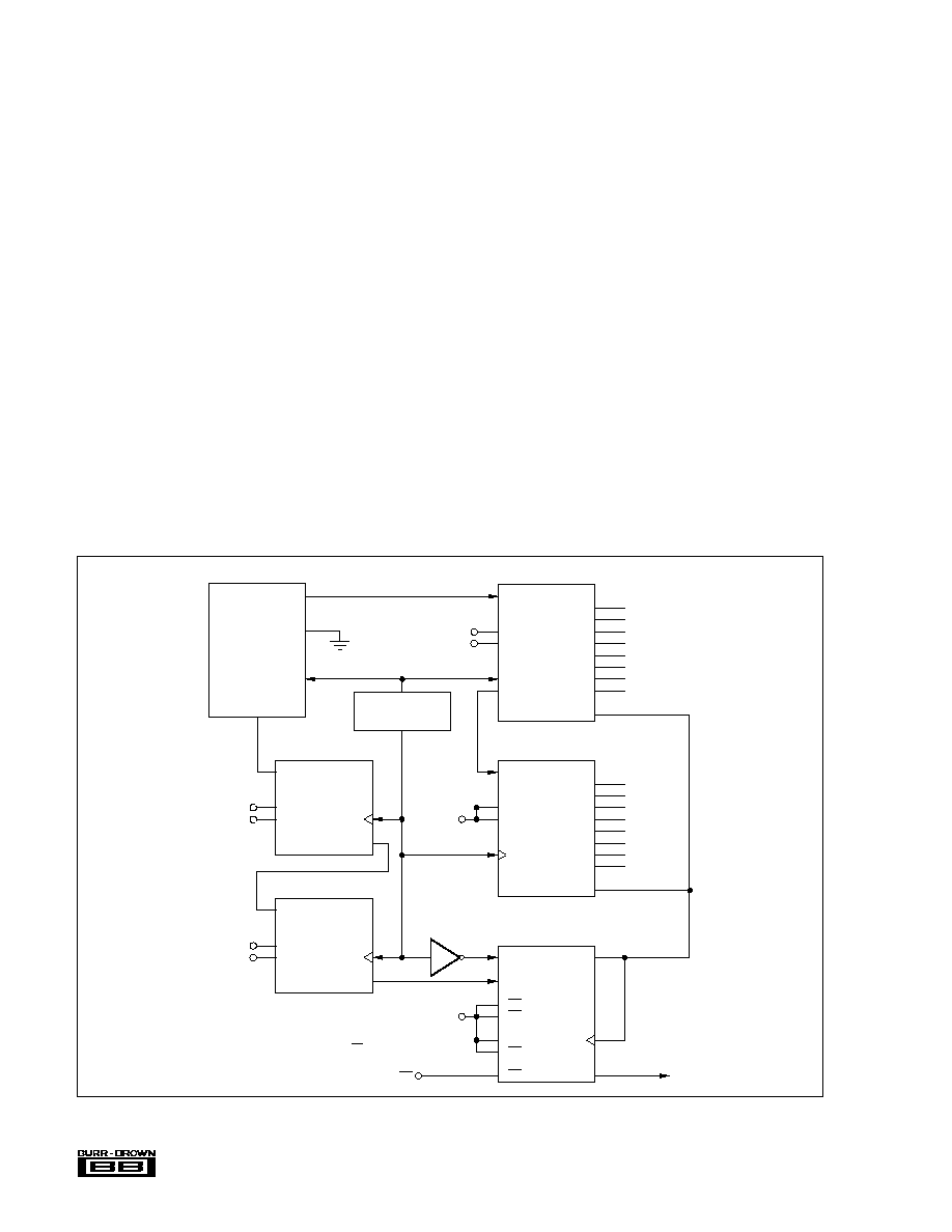
FIGURE 4. Output Structure of DSP102.
DATA TRANSFER
The internal A/Ds generate 18 bits of data, transmitting the
data MSB first. When read by a DSP IC programmed to
accept 16 bits of data, the first 16 MSB bits of data from the
DSP101, or each channel of the DSP102, will be shifted into
the processor's input shift register, and the last two least
significant bits of data from the A/D will be ignored,
although they will still be present on the serial data line.
When the DSP processor is programmed to accept words of
more than 16-bit length (typically 24-bit or 32-bit), the
DSP101 and DSP102 will transmit the full 18-bit conversion
results, after which the information input on the TAG input
(or TAGA and TAGB on the DSP102) will be appended to
the output word. (See Tag Feature below.)
In the Cascade Mode, the DSP102 will first transmit the 16
MSBs from channel A, followed by the full 18 bits from
channel B, although DSP processors programmed to accept
32 bits of data will ignore the final two bits of information
on Channel B. See the DSP102 Cascade Mode section below
for details of the Cascade mode.
DATA SYNCHRONIZATION
A convert command both initiates a conversion and starts
the process for transmitting data from the previous conver-
sion. Convert commands can come at any time, completely
asynchronous to the conversion clock or the bit clock, and
the conversion clock may also be independent of the bit
clock. The DSP101 and DSP102 internally synchronize the
output data, Sync pulse, and Tag inputs to the bit clock.
While the convert command, conversion clock and bit clock
can be asynchronous, system performance is usually en-
hanced by synchronizing all of them to a system master
clock, whenever the application permits. This minimizes
changes in digital loads and currents when the critical S/H
transition and A/D bit decisions are occurring. Within the
DSP101 and DSP102 themselves, running asynchronous
convert commands, conversion clocks and bit clocks typi-
cally degrades performance only several dB, as shown in the
various typical performance curves, but the system board
design can easily have more effect.
When a convert command is received, the internal logic
generates an appropriate Sync pulse, synchronized to XCLK,
as shown in Figure 1. The output Sync pulse will be active
High or active Low depending on whether a HIGH or a
LOW, respectively, is input at SSF (pin 12).
The convert command also causes the conversion results
from the previous conversion to be loaded into the output
shift register, synchronous to XCLK. Figure 4 shows the
operation of the internal data shift registers on the DSP102.
The DSP101 is basically similar, but includes only the top of
the figure, showing the SOUTA path.
(LSB)
18
16
14
12
10
8
6
4
2
(MSB)
1
18-bit Register
Channel B Conversion Results from SAR
Shift/Load
(1)
CONV
CLKIN
XCLK
TAGB
18
(LSB)
D
1
16
14
12
10
8
6
4
2
1
(MSB)
18-bit Register
Channel A Conversion Results from SAR
CONV
CLKIN
XCLK
Shift/Load
(1)
TAGA
18-bit Shift Register
18-bit Shift Register
18-bit Shift Register
18-bit Shift Register
SOUTA
SOUTB
D
2
E
CASC
NOTE: (1) Signal internal to DSP101/DSP102 which also generates SYNC pulse.
RCK
D1
D1
D
RCK
D

®
DSP101/102
11
During the internal successive approximation conversion
process, the conversion results are shifted into the input shift
registers of the output stage on the DSP102. A new convert
command latches that data into the 18-bit parallel latches
shown. The internal signal that also generates the Sync
pulse, labeled "Shift/Load" in Figure 4, synchronously loads
the conversion data into the output shift register on the rising
edge of XCLK. The conversion results are then clocked out
of the shift register on subsequent rising edges of XCLK.
DATA TRANSFER CLOCK
XCLK is the data transfer clock, or bit clock, for the system,
and is an input for the DSP101 or DSP102. This input is
TTL- and 74HC-level compatible. The serial data and SYNC
outputs are synchronized internally to this clock, with data
valid on the rising edge of XCLK, per the timing shown in
Figure 1. Data input on pin 18 (TAG) on the DSP101, or on
pins 18 and 19 on the DSP102 (TAGA and TAGB), will be
clocked into the output shift register on the rising edge of
XCLK, as discussed in the Tag Feature section.
CONVERSION CLOCK
The analog-to-digital converter sections in the DSP101 and
DSP102 were designed to provide accurate conversions
under worst case conditions of supplies, temperatures, etc.
In order to achieve a full 200kHz sampling capability, they
were designed to use a 33% duty cycle conversion clock
(CLKIN on pin 10) as shown in Figure 1. The clock is LOW
FIGURE 6. DSP101 or DSP102 Power Supply Connections.
FIGURE 5. DSP101 or DSP102 Conversion Clock Circuit.
To other
DSP102's CLKIN for
synchronous operation
1M
Crystal is CTS Knight MP122 12.288MHz,
20pF load, series resonant mode.
12.288MHz
÷3
SAR Clock
Control
10pF
10
11
DSP101 or DSP102
CLKOUT
OSC2
OSC1
13
14
10pF
CLKIN
long enough for internal analog circuitry to settle suffi-
ciently between bit decisions to insure rated accuracy. Bit
decisions in the A/D are then made on the rising edge of
CLKIN.
1
2
3
4
5
6
7
8
9
10
11
12
13
14
28
27
26
25
24
23
22
21
20
19
18
17
16
15
10µF
10µF
0.1µF
VPOTA
AGND
REF
VPOTB
10µF
DSP101 or DSP102
+
+
+
+
10µF
0.01µF
5V Analog
+5V Analog
+5V Digital
V
V +
DGND
DGND
V
A
A
D
= Analog Ground
= Digital Ground
(1)
(1)
NOTES: (1) Pin 1 and pin 26 must be bypassed with 10µF tantalum capacitors, on both the DSP101 and DSP102.
(2) Protection from power supply momentary overrange.
10
(2)

®
DSP101/102
12
When a convert command is received, the DSP101 or
DSP102 immediately switches the sampling capacitors to
the hold state, and then internally gates the conversion clock
to the A/D appropriately. Allowing a minimum of 24 CLKIN
pulses between conversions insures that there is sufficient
time for complete, accurate conversions, and allows the
input sampling capacitor to fully acquire the next sample,
regardless of the timing between the convert command and
CLKIN.
In most applications, CLKIN (pin 10) can be driven from a
50% duty cycle clock without performance degradation.
During characterization of the DSP101 and DSP102, the
performance of a number of parts was measured under
various conditions with a 4.8MHz, 50% duty cycle input to
CLKIN at a full 200kHz conversion rate without noticeable
degradation.
OSCILLATOR INPUTS AND CLKOUT
The DSP101 or DSP102 can generate a 33% duty cycle
conversion clock output on CLKOUT (pin 11). This is
accomplished by dividing by three a clock from either an
external 74HC-level clock or from a crystal oscillator.
CLKOUT can deliver
±
2mA, and can be used to drive
multiple DSP101 or DSP102 CLKINs. See Figure 1 for the
timing relationship between OSC1 and CLKOUT.
To use an external 74HC-level clock, drive the clock into
OSC1 (pin 13), and leave OSC2 (pin 14) unconnected.
To use a crystal oscillator to generate the conversion clock,
refer to Figure 5. Connect the oscillator between OSC1 and
OSC2. OSC2 provides the drive for the crystal oscillator.
This pin cannot be used elsewhere in the system.
FIGURE 7. DSP101 or DSP102 Input Buffering.
1
2
3
4
5
6
7
8
9
10
11
12
13
14
28
27
26
25
24
23
22
21
20
19
18
17
16
15
10µF
10µF
0.1µF
VPOTA
VINA
REF
VPOTB
VINB
150
220pF
+
7
5
6
1/2
OPA2604
Analog
Input B
150
+
1/2
OPA2604
Analog
Input A
2.2µF
2.2µF
5V
+5V
3
2
4
8
220pF
DSP101 or DSP102
(1)
+
+
+
+
1
Leave out on DSP101
(1)
NOTE: (1) On DSP101, pin 25 is not internally
connected. Pin 26 must still be bypassed with
the 10µF Tantalum capacitor.
If CLKOUT is not used, both it and OSC2 should be left
unconnected, and OSC1 should be grounded.
TAG FEATURE
Figure 4 shows the implementation of the TAG feature on
the DSP101 and DSP102. When a convert command is
received, the internal Shift/Load signal loads conversion
result data into the output shift register synchronous to
XCLK. Between convert commands, the information input
on TAG (on the DSP101) or on TAGA and TAGB (on the
DSP102) will be clocked into the output shift register on the
rising edges of XCLK. Since this is an 18-bit shift register,
the data input on the Tag lines will be output on SOUT
(DSP101) or SOUTA and SOUTB (DSP102) delayed by 18
bit clocks.
The Tag Feature can be used in various ways. The Tag
inputs can be tied HIGH or LOW to differentiate between
two converters in a system. As discussed in the Applications
section below, the Tag feature can be used to append to the
serial output data word information on multiplexer channel
address, or other digital data related to the input signal (such
as the setting on a programmable gain amplifier.) Another
option would be to daisy-chain multiple DSP101 or DSP102
converters, linking the serial output of one to the Tag input
of the next. This can simplify the transmission of data from
multiple A/Ds over a single optical isolation channel.
DSP102 CASCADE MODE
If pin 22 (CASC) is tied HIGH, the DSP102 will be in the
Cascade Mode. In this mode, when a convert command is
received, the DSP102 will transmit a 32-bit data word on pin

®
DSP101/102
13
20 (SOUTA) containing data for both input channels in two
16-bit words. Referring to Figure 1, the first 16 bits of data
will be the results for channel A, followed by 16 bits of
information for channel B. The data will be transferred MSB
first. A convert command at time (t) will initiate the trans-
mission of the results of the conversion initiated at time
(t 1).
From the descriptions above of the internal shift registers
shown in Figure 4, it can be seen that the DSP102 in the
Cascade Mode actually continues to shift out data after the
32nd bit of the data word. The next two bits clocked out will
be the last two data bits from the full 18-bit conversion on
channel B, after which the information output on SOUTA
will be the information clocked into TAGB 35 bit clock
cycles earlier.
In the Cascade mode on the DSP102, SOUTB will still
output channel B conversion data and tag data as usual.
ANALOG PERFORMANCE
LINEARITY
The DSP101 and DSP102 are optimized for signal process-
ing applications with wide dynamic range requirements.
Linearity is trimmed for best performance in the range
around 0V, which is critical for handling low amplitude
signals. The DSP101 and DSP102 typically have integral
and differential non-linearity below
±
0.003% in the input
range of
±
0.7V, with there being no missing codes at the
14-bit level in this range. Over the full
±
2.75V input range,
the largest non-linearities are centered around the bit #2
transition points at +1.375V and 1.375V levels.
NOISE AND BIPOLAR ZERO ERROR
The equivalent input noise and bipolar zero error of the
DSP101 and DSP102 is shown in the typical performance
section for both channels on a DSP102. The inputs to both
channels were grounded, and the results of 5,000 conver-
sions was recorded. The data shown is binned at the 16-bit
level. The noise results from all sources in the circuit,
including clocks, reference noise, etc.
In a theoretically ideal converter with no offset and no noise,
the results of all 5,000 conversion for each channel would lie
in the bin corresponding to bipolar zero, code 0000. The
typical DSP101 or DSP102 will have offset errors in the
range of 1 to 2mV, and the two channels on the DSP102 will
be matched closer than 2mV. The DSP102 shown in the
typical performance section has the worst offset, 0.8mV,
on channel A, with channel B being less than 1mV different,
and the three sigma noise on either channel being less than
250
µ
V.
INPUT BANDWIDTH
From the typical performance curves, it can be seen that
there is very little degradation in Signal-to-(Noise + Distor-
tion) for input signals up to 100kHz. The wideband sampling
input typically maintains a 60dB Signal-to-(Noise + Distor-
tion) Ratio undersampling 500kHz input signals.
LAYOUT CONSIDERATIONS
Because of the high resolution, linearity and speed of the
DSP101 and DSP102, system design problems such as
ground path resistance, contact resistance and power supply
quality become very important.
FIGURE 8. DSP101 or DSP102 Optional MSB and Offset Adjust.
1
2
3
4
5
6
7
8
9
10
11
12
13
14
28
27
26
25
24
23
22
21
20
19
18
17
16
15
0.1µF
VPOTA
MSBA
VOSA
REF
VPOTB
MSBB
VOSB
150k
25k
10µF
47k
25k
+
47k
25k
10µF
150k
25k
+
DSP101 or DSP102
(1)
47k
0.01µF
0.01µF
0.01µF
47k
0.01µF
Leave out on DSP101
(1)
NOTE: (1) On DSP101, pins 23 and 24 are
not internally connected. Pin 26 must still be
bypassed with the 10µF Tantalum capacitor.
®
DSP101/102
14
Optimal dynamic performance is achieved by soldering the
parts directly into boards, to keep the A/Ds as close as
possible to ground. The use of sockets will often degrade AC
performance. Zero-Insertion-Force sockets are particularly
poor because longer lead lengths create inductance.
Short traces on the board, and bypass capacitors as close as
possible to the A/D, will further improve dynamic perfor-
mance.
GROUNDS
To achieve the maximum performance from the DSP101 or
DSP102, care should be taken to minimize the effect of
changes in current flowing in the system grounds, particu-
larly while bit decisions are being made in the successive
approximation converter's comparator. Pin 28 (AGND) on
both the DSP101 and the DSP102 is the most critical, and
care should be taken to make this pin as close as possible to
the same potential as the system analog ground.
Whenever possible, it is strongly recommended that separate
analog and digital ground planes be used. With an LSB level
of 84
µ
V at the 16-bit level, and one-quarter of that at the
18-bit level, the currents switched in a typical DSP system
can easily corrupt the accuracy of the A/Ds unless great care
is taken to analyze and design for current flows.
FIGURE 9. Driving a 16-bit Parallel Port from the DSP101.
TTL Bit
Clock
20
12
Serial Data
74HC594
(1)
DSP101
SOUT
SSF
XCLK
SR CLK
QH
SR CLR
R CLR
10
13
15
1
2
3
4
5
6
7
12
SYNC
D15 (LSB)
D14
D13
D12
D11
D10
D9
D8
QH
RCK
QA
D1
74HC164
D2
CLR
Serial Data
74HC594
(1)
SR CLK
SR CLR
R CLR
10
13
11
15
1
2
3
4
5
6
7
12
D7
D6
D5
D4
D3
D2
D1
D0 (MSB)
QH
RCK
QA
+5V
8
13
+5V
1
2
9
CLK
Q7
15
D1
74HC164
D2
CLR
CLK1
74HC74
5
11
9
CLK2
Q2
Q1
+5V
8
13
+5V
1
2
9
CLK
Q7
4
1
12
10
13
D1
S1
R1
D2
S2
R2
+5V
RD
Data Valid Signal
NOTE: (1) Substituting
74HC595s provides three
state outputs, with pin 13 (OE)
used to enable the parallel
data lines.
+5V
+5V
2
3
14
11
9
14
16
+5V
HC04
POWER SUPPLY DECOUPLING
All of the supplies should be decoupled to the appropriate
grounds using tantalum capacitors in parallel with ceramic
capacitors, as shown in Figure 6. For optimum performance
of any high resolution A/D, all of the supplies should be as
clean as possible. If separate digital and analog supplies are
available in a system, care should be taken to insure that the
difference between the analog and the digital supplies is not
more than 0.5V for more than a few hundred milliseconds,
as may occur at power-on.
INPUT SIGNAL CONDITIONING
To avoid introducing distortion, the DSP101 and DSP102
analog inputs must be driven by a source with low imped-
ance over the input bandwidth needed in the application. Op
amps such as the NE5532 or Burr-Brown's OPA2604 work
well over audio bandwidths. Figure 7 shows an appropriate
input driver circuit. The 150
and 220pF shown on the input
help reduce the dynamic load on the input signal condition-
ing amp in front of the A/D, since all switched capacitor
array architectures exhibit fast changes in input current load
as the input sampling switch is opened and closed. These
dynamic changes in the load can affect any signal condition-
ing circuit at the input. Other R and C combinations can be

®
DSP101/102
15
used, but the resistor should not exceed 200
, or the output
settling time of the signal conditioning amplifier may be too
long.
EXTERNAL ADJUSTMENTS
All of the specifications for the DSP101 and DSP102, plus
the typical performance curves, are based on the perfor-
mance of these A/Ds without external trims. In most appli-
cations, external trims are not required.
OFFSET ADJUST
Where required by specific applications, offsets can be ad-
justed using the circuit of Figure 8. When not adjusted, VOS
(pin 4) on the DSP101, and VOSA (pin 4) and VOSB (pin 23)
on the DSP102, should be left open. If these pins are con-
nected to traces on the board, they should be bypassed to
ground with 0.01
µ
F capacitors, as close as possible to the A/D.
To trim offset, one alternative is to ground the analog input
while converting continually. Then adjust the trimpot (on
VOS for the DSP101, on VOSA and VOSB for the DSP102)
until the output code is toggling between the codes FFFF and
0000 (Hex) at the 16-bit level (3FFFF and 00000 at the
18-bit level.) This will center the offset at 1/2 LSB below
0V, which is respectively 42
µ
V or 10
µ
V at the 16- and
18-bit levels.
The offset can also be adjusted by providing a sine wave to
the A/D input. Using FFT, or even simple averaging of
several thousand conversion results at a time, the trimpots
can be adjusted until there is no DC offset of the signal.
Grounding the input, or providing the sine wave, as far in
front of the A/D as possible allows offset from intervening
signal conditioning components to be also corrected by this
procedure.
MSB ADJUST
In most applications, adjustment of the Most Significant Bit
weight will not be required. When not adjusted, MSB (pin 3)
on the DSP101, and MSBA (pin 3) and MSBB (pin 24) on
the DSP102, should be left open. If these pins are connected
to traces on the board, they should be bypassed to ground
with 0.01
µ
F capacitors, as close as possible to the A/D.
MSB (pin 3) on the DSP101, and MSBA (pin 3) and MSBB
(pin 24) on the DSP102, are internally connected to a
resistor divider network that is used to laser-trim the weight
FIGURE 10. A Complete Eight-Channel Analog Input System Using the DSP202 and the HI-508A.
CI
OPA627
Out
EN
A
0
A
1
A
2
In
1
In
2
In
3
In
4
In
5
In
6
In
7
In
8
D
C
B
A
LD
CLK
8D
7D
6D
5D
4D
3D
2D
1D
H
G
F
E
D
C
B
A
SOUT
VIN
SSF
QD
QC
QB
QA
CL
CO
EP
ET
6
11
5
12
4
13
3
14
9
1
8Q
7Q
6Q
5Q
4Q
3Q
2Q
1Q
CLK
74HC574
15
74HC163
74HC166
SI
S/L
CLK
CL
QH
9
8
7
6
5
12
13
14
15
16
14
12
11
10
5
4
3
2
1
15
17
18
19
4
3
2
SYNC
XCLK
TAG
CONV
2
12
15
16
18
20
21
DSP101
9
6
7
7
10
2
1
11
150
C
1
220pF
HI-508A
8
2
1
16
15
9
10
11
12
7
6
5
4
+5V
+5V
+5V
5
4
74HC221
3
+5V
B
A
CL
2
1
R/C
CE
Q
Q
13
4
14
15
1000pF
C
4
+5V
R
2
4.7k
13
R
1
NOTE: (1) Must be low source impedance
with unused inputs tied to ground.
Analog Inputs
(1)
Convert Command
(Positive Edge Triggered)
6
2
3
OE
Serial Data Out

®
DSP101/102
16
of the MSB capacitor in the CDAC. These pins are nomi-
nally at +100mV after laser-trimming during manufacturing.
They can handle external inputs up to about one diode drop
below ground (0.6V) before internal clamping circuitry is
triggered.
Figure 8 shows an appropriate circuit for adjusting the
weight of the most significant bit to minimize differential
non-linearity at the critical major-carry transition. To adjust,
provide a small amplitude sine wave to the selected A/D
input pin while converting continually, and adjust for maxi-
mum Signal-to-(Noise + Distortion) ratio, using appropriate
signal analysis software.
GAIN ADJUST
If circuit gain needs to be adjusted in hardware, rather than
in system software, appropriate trimpots should be included
in the analog signal conditioning section in front of the
DSP101 or DSP102. No specific gain adjust circuitry is
included in the parts.
APPLICATIONS
INTERFACING DSP101 TO PARALLEL PORTS
Figure 9 shows a circuit for converting the serial output data
from the DSP101 into 16 bits of parallel data, within the
timing constraints of the serial bit-stream from the DSP101.
In many applications, this circuit can be easily incorporated
into gate arrays or other programmed logic circuits already
used in the system, since the extra gate count is not high.
This circuit adds an additional pipeline delay to the conver-
sion data, so that the parallel data from a conversion at time
(t) is valid one conversion cycle plus 17 XCLK clocks later
(at t+1 plus 17 times XCLK). A convert command at time
(t+1) generates a Sync and begins transmitting serial data
from SOUT. The serial data is shifted into the 74HC594
shift registers, and Sync is shifted through the 74HC164
shift registers. The Q1 output of the 74HC74 dual D-type
flip-flops clocks the conversion data into the output register
of the 74HC594s, and triggers a data valid signal on its Q2
output. The user can then read the data at any time before the
next conversion is started, and the Read signal will reset the
data valid output from Q2.
In many systems, galvanic isolation of signals is required.
Using opto-couplers on the serial data lines in Figure 9
allows a fully isolated system to be built using a DSP101 and
only three couplers across the barrier (for serial data, XCLK
and SYNC.)
MULTIPLEXING INPUTS TO THE DSP101
Figure 10 shows a complete circuit for sequentially scanning
eight analog input channels with a single DSP101, and using
the Tag feature on the DSP101 to append the multiplexer
channel address to the serial output conversion results.
The circuit in Figure 10 includes the required digital logic
and timing logic. The 74HC163 counter provides the scan
sequence to the Burr-Brown HI-508A analog multiplexer. In
order to allow the HI-508A enough time to switch to the next
channel and settle before the DSP101 begins a conversion,
a 74HC221 one-shot introduces a 3
µ
s delay for the DSP101
convert command input.
The Burr-Brown OPA627 provides a low impedance source
for the DSP101, buffering it from the output impedance of
FIGURE 11. Analog Input and Analog Output System.
TTL Bit
Clock
12
13
11
9
10
15
XCLK
SIN
SYNC
SSF
SWL
CONV
±3V Analog Output
21
VOUT
DSP201
Conversion Rate
Generator
XCLK
SOUT
SYNC
SSF
DSP101
SSF
SWL
16
20
15
12
2
±2.75V
Analog Input
CLKR
DATA IN
SYNC
XCLK
DATA OUT
SYNC
SSF
(2)
VIN
Digital Signal
Processor IC
21
CONV
(1)
(2)
(3)
DSP PROCESSOR
SYNC FORMAT
SERIAL I/O WORD
SSF
(2)
SWL
(3)
DSP32C, DSP16
Active Low
16 Bits
LOW
HIGH
DSP56001
Active High
24 Bits
HIGH
LOW
DSP56001
Active High
16 Bits
HIGH
HIGH
TMS320C25/C30
Active High
16 Bits
HIGH
HIGH
ADSP2101/2105
Active High
16 Bits
HIGH
HIGH
(1) See Burr-Brown
DSP201/DSP202
product data sheet
for full description of
this DAC.

®
DSP101/102
17
the multiplexer. This unity-gain buffer minimizes distortion,
taking full advantage of the resolution and bandwidth of the
DSP101.
The 74HC574D register delays the multiplexer address data
by one conversion before appending the channel data to the
serial conversion results from the DSP101. This attaches the
channel address to the correct conversion results. Since the
channel scanning shown in Figure 10 is sequential, this
delay latch could be left out and software could recognize
that the time (t) conversion results have the MUX address
from the time (t-1) conversion appended. However, for
systems using non-sequential scan lists, this delay latch is
essential to maintain the conversion data and channel ad-
dress integrity.
The 74HC166 synchronous loading shift register loads the
channel address tag data into the shift register on the rising
edge of the bit clock, in conjunction with the Sync output of
the DSP101. The channel address tag data is then clocked
into the DSP101 Tag input (pin 18) by the bit clock, while
the conversion data is clocked out the other end of the
DSP101 shift register (discussed in another section of this
data sheet.)
Figure 10 was developed and tested using a Burr-Brown
ZPB34 DSP board, which contains an AT&T DSP32C, so
that the SYNC output is programmed to be active LOW. The
circuit needs to be modified for DSP processors from ADI,
TI, and Motorola, which use active HIGH Sync pulses. For
these processors, tie SSF (pin 12) on the DSP101 HIGH, and
use a 74HC04 hex inverter to invert the Sync signal to the
74HC574 and 74HC166.
The same basic circuit can be duplicated to drive two
channels in a DSP102, or can be easily modified for more or
less than eight channels of analog input.
USING DSP101 AND DSP102 WITH
TEXAS INSTRUMENTS DSP ICS
Figures 11 thru 17 show various ways to use the DSP101
and DSP102 with DSP ICs from the Texas Instruments
TMS320Cxx series. For simplicity, all of these circuits are
FIGURE 13. Using DSP102 with TMS320C30 in Cascade Mode.
16
15
20
17
22
12
21
CLKR -0
FSR-0
DR-0
±2.75V Analog Input
Channel A
2
25
VINA
VINB
TMS320C30
Conversion Rate
Generator
DSP102
XCLK
SYNC
SOUTA
SOUTB
CASC
SSF
CONV
±2.75V Analog Input
Channel B
+5V
+5V
NOTE: Serial port 0 programmed
for 32-bit data.
TTL Bit
Clock
NC
FIGURE 12. Using DSP102 with TMS320C30.
TTL Bit
Clock
16
15
20
17
22
12
21
CLKR
±2.75V Analog Input
Channel A
2
VINA
VINB
TMS320C30
Conversion Rate
Generator
DSP102
25
XCLK
SYNC
SOUTA
SOUTB
CASC
SSF
CONV
±2.75V Analog Input
Channel B
DR-0
DR-1
FSR-0
FSR-1
+5V

®
DSP101/102
18
based on using the TME320Cxx in the mode where SSF
(Select Synch Format, pin 12) is tied HIGH, so that there is
an active High synchronization pulse generated by the
DSP101 or DSP102 after receiving a convert command. The
synchronization pulse can be changed to active Low simply
by making SSF LOW, where appropriate, without changing
the basic operation of the A/Ds.
In all cases, the DSP101 and DSP102 will transmit data
MSB-first, and the TMS320Cxx needs to be programmed
for this.
Figure 11 shows a circuit for using the TMS320C25 or
TMS320C30 in a complete analog input and analog output
system using the DSP101 along with the Burr-Brown DSP201
D/A.
FIGURE 14. Two-Channel Analog Input and Output System with TMS320C30.
TTL Bit
Clock
12
11
9
10
16
15
XCLK
SYNC
SSF
SWL
CASC
CONV
±3V Analog Output
Channel A
21
5
VOUTA
VOUTB
DSP202
Conversion Rate
Generator
XCLK
SYNC
SSF
CASC
CONV
DSP102
+5V
+5V
16
15
12
22
21
±2.75V Analog Input
Channel A
DR-0
DR-1
CLKX-0
CLKX-1
±3V Analog Output
Channel B
DX-0
DX-1
FSX-0
FSX-1
CLKR-0
CLKR-1
FSR-0
FSR-1
+5V
TMS320C30
VINA
VINB
±2.75V Analog Input
Channel B
2
25
NOTES: (1) Sample rate on DSP102 and DSP202 may differ. (2) Analog Devices ADSP2101 may be used. SPORT1 and SPORT2
are used for serial MSB first communication. (3) See Burr-Brown DSP201/DSP202 product data sheet for full description of this DAC.
(1)
(3)
SOUTA
SOUTB
20
17
SINA
SINB
13
14
FIGURE 15. Two-Channel Analog Input and Output System with TMS320C30 in Cascade Mode.
TTL Bit
Clock
12
13
14
11
9
10
16
15
XCLK
SINA
SINB
SYNC
SSF
SWL
CASC
CONV
±3V Analog Output
Channel A
21
5
VOUTA
VOUTB
DSP202
Conversion Rate
Generator
XCLK
SOUTA
SOUTB
SYNC
SSF
CASC
CONV
DSP102
+5V
+5V
+5V
16
20
17
15
12
22
21
±2.75V Analog Input
Channel A
CLKR-0
DR-0
±3V Analog Output
Channel B
CLKX-0
DX-0
FSR-0
+5V
+5V
TMS320C30
VINA
VINB
±2.75V Analog Input
Channel B
2
25
NOTES: (1) Program TMS320C30 for 32-bit mode. (2) Sample rate on DSP102 and DSP202 may differ. (3) DSP32C may be used in this mode.
(4) See Burr-Brown DSP201/202 product data sheet for full description of this DAC.
FSX-0
NC
(2)
(4)

®
DSP101/102
19
SERIAL PORT
Port Global Control Register
0x0EBC040
FSX/DX/CLKX Port Control Register
0x00000111
FSR/DR/CLKR Port Control Register
0x00000111
Receive/Transmit Timer Control Register
0x0000000F
TIMER
Timer Global Control Register
0x000002C1
Timer Period Register
0x000000B5
NOTE: Assumes TMS320C31 has 32MHz Master Clock.
USING TMS320C31 TO GENERATE
ALL CONTROL SIGNALS
Figure 17 shows a circuit for using the TMS320C31 with a
DSP102 and a Burr-Brown DSP202 D/A to provide a two
channel analog I/O system. The flexibility of the TMS320C31
allows it to generate the data transfer clock (XCLK) and the
Convert Command, minimizing additional circuitry and syn-
chronizing the timing signals to the processor's master
clock. In this circuit, the DSP102 and DSP202 are used in
their Cascade modes, transmitting and receiving two chan-
nels of data in a single 32-bit word. (See the Cascade Mode
section above.)
Table II shows how to set up the circuit in Figure 17 for a
44.1kHz conversion rate for both channels of the DSP102
A/D and both channels of the DSP202 D/A. Both inputs and
outputs will be simultaneously converted.
XCLK
SYNC
SOUT
SSF
CONV
VIN
DSP101
TTL Bit
Clock
Conversion Rate
Generator
XCLK
FSX
TXD
±2.75V Analog Input
16
15
20
12
21
+5V
NOTES: (1) TMS320C25 FSR external, 16-bit data.
2
TMS320C25
FIGURE 16. Using DSP101 with TMS320C25.
FIGURE 17. Two Channel Analog I/O Using TMS320C31.
1M
XCLK
SYNC
SSF
SWL
CASC
CONV
±3V Analog Output
VOUTA
DSP202
XCLK
SYNC
CASC
DSP102
±2.75V Analog Input
DR0
FSR0
DX0
FSX0
+5V
VINA
TMS3200C31
CONV
VINB
OSC2
OSC1
TCLK0
+5V
Channel A
±3V Analog Output
VOUTB
+5V
+5V
+5V
10pF
10pF
12.288MHz
±2.75V Analog Input
Channel B
Channel A
Channel B
SINA
SINB
SOUTA
SOUTB
SSF
NC
CLKR0
CLKX0
TABLE II. TMS320C31 Register Settings for 44.1kHz Con-
version Rate in Figure 17.

®
DSP101/102
20
USING DSP101 AND DSP102
WITH MOTOROLA DSP ICS
Figure 18 shows how to use the DSP101 with a Motorola
DSP56001. Using the DSP102 requires using two
DSP56001s. The DSP56001 needs to be programmed to
receive data MSB-first with SYNC in the Bit Mode.
SSF (pin 12) needs to be tied HIGH for using either the
DSP101 or the DSP102 with DSP56001s. This will cause
the DSP101 or DSP102 to transmit an appropriate active
High synchronization pulse on SYNC (pin 15) after a con-
vert command is received by the A/D. Timing is shown in
Figure 1.
USING DSP101 AND DSP102 WITH AT&T DSP ICS
Figures 11, 19, 20, and 21 show how to use the DSP101 and
DSP102 with the DSP16 and DSP32C in different modes.
The AT&T processors need to be programmed to accept
data MSB-first, and the DSP101 or DSP102 needs to have
SSF (pin 12) tied LOW, so that an appropriate active Low
synchronization pulse will be transmitted by the A/D after a
convert command is received.
Figures 19 and 20 show the DSP32C and DSP16 respec-
tively used with the DSP101 to handle a single analog input
channel.
Figure 21 shows how to transmit to a single DSP32C
conversion results from both DSP102 channels in a single
32-bit word, using the Cascade mode on the A/D.
Figure 11 indicates how to build a complete analog input and
analog output system using a DSP32C or DSP16 with a
DSP101 and a Burr-Brown DSP201 D/A.
XCLK
SYNC
SOUT
SSF
CONV
VIN
DSP101
TTL Bit
Clock
Conversion Rate
Generator
SCK
FSR (SC2)
SRD
DSP56001
±2.75V Analog Input
16
15
20
12
21
+5V
NOTES: (1) DSP56001 programmed for MSB bit first data. (2) DSP56001 data may be either 16-bit or 24-bit.
2
FIGURE 18. Using DSP101 with DSP56001.
XCLK
SYNC
SOUT
VIN
DSP101
TTL Bit
Clock
Conversion Rate
Generator
ICK
ILD
DATA IN
±2.75V Analog Input
16
15
20
NOTE: (1) DSP32C programmed for MSB bit first 16-bit data.
2
DSP32C
SSF
CONV
12
21
FIGURE 19. Using DSP101 with DSP32C.

®
DSP101/102
21
USING DSP101 AND DSP102 WITH ADI DSP ICS
When using the DSP101 or DSP102 with the fixed-point
ADSP21xx series, the processors need to be programmed to
receive data MSB-first.
Figure 22 shows how to use the DSP102 with an ADSP2101
to provide a two-channel simultaneous sampling system.
Figure 23 shows the connections required to generate an
analog input channel using an ADSP2105 with the DSP101.
The same basic circuit can be used to connect a DSP101 to
the ADSP2101.
Figure 11 indicates how to build a complete analog I/O
system using either the ADSP2101 or the ADSP2105 with a
DSP101 and a Burr-Brown DSP201 D/A.
The two serial ports on the ADSP2101 can also be used with
the DSP102 and the Burr-Brown DSP202 D/A to make two
complete analog I/O channels, as indicated in footnote 2 of
Figure 14.
TTL Bit
Clock
16
20
15
12
ICK
DATA IN
ILD
±2.75V Analog Input
2
VIN
DSP16
Conversion Rate
Generator
DSP101
XCLK
SOUT
SYNC
SSF
NOTE: DSP16 programmed for MSB bit first, 16-bit data.
21
CONV
FIGURE 20. Using DSP101 with DSP16.
FIGURE 21. Using DSP102 with DSP32C in Cascade Mode.
XCLK
SYNC
SOUTA
SOUTB
CASC
SSF
CONV
VINA
VINB
DSP102
TTL Bit
Clock
Conversion Rate
Generator
ICK
ILD
DATA IN
±2.75V Analog Input
Channel A
16
15
20
17
22
12
21
NOTES: (1) DSP32C programmed 32-bit data MSB bit first. (2) Data format is Channel A, 16 bits, MSB first, then Channel B.
2
DSP32C
±2.75V Analog Input
Channel B
25
NC
+5V

®
DSP101/102
22
TTL Bit
Clock
16
15
20
17
DR-0
DR-1
±2.75V Analog Input
Channel A
2
25
VINA
VINB
ADSP-2101
Conversion Rate
Generator
DSP102
XCLK
SYNC
SOUTA
SOUTB
±2.75V Analog Input
Channel B
+5V
SCLK-0
SCLK-1
RFS-0
RFS-1
12
21
SSF
CONV
22
CASC
FIGURE 22. Using DSP102 with ADSP-2101.
FIGURE 23. Using DSP101 with ADSP-2105.
TTL Bit
Clock
16
20
15
12
21
±2.75V Analog Input
2
VIN
ADSP-2105
Conversion Rate
Generator
DSP101
XCLK
SOUT
SYNC
SSF
CONV
+5V
SCLK
DR
RFS
DEM-DSP102/202 EVALUATION BOARD
An evaluation fixture, the DEM-DSP102/202, is available to
simplify evaluation of the DSP101 and DSP102, and the
companion digital-to-analog converters, the single DSP201
and dual DSP202. The DEM-DSP102/202 comes complete
with a socketed DSP102 and DSP202, a breadboard area,
TTL I/O headers and differential line drivers for data trans-
fer options, a complete clocking circuit for the conversion
clock and bit clock, and analog filter modules. The board
makes it easy to go from design concept to working proto-
type of a DSP-based system, offering two complete analog
I/O channels.
Contact your local Burr-Brown representative for a full data
sheet on the DEM-DSP102/202.