
DAC7617
Quad, Serial Input, 12-Bit, Voltage Output
DIGITAL-TO-ANALOG CONVERTER
FEATURES
q
LOW POWER: 3mW
q
SETTLING TIME: 10
µ
s to 0.012%
q
12-BIT LINEARITY AND MONOTONICITY:
40
°
C to +85
°
C
q
DOUBLE-BUFFERED DATA INPUTS
q
SO-16 or SSOP-20 PACKAGES
q
SINGLE-SUPPLY +3V OPERATION
APPLICATIONS
q
PROCESS CONTROL
q
ATE PIN ELECTRONICS
q
CLOSED-LOOP SERVO-CONTROL
q
MOTOR CONTROL
q
DATA ACQUISITION SYSTEMS
q
DAC-PER-PIN PROGRAMMERS
DESCRIPTION
The DAC7617 is a quad, serial input, 12-bit, voltage
output Digital-to-Analog Converter (DAC) with guar-
anteed 12-bit monotonic performance over the 40
°
C
to +85
°
C temperature range. An asynchronous reset
clears all registers to either mid-scale (800
H
) or zero-
scale (000
H
), selectable via the RESETSEL pin. The
individual DAC inputs are double buffered to allow
for simultaneous update of all DAC outputs. The
device is powered from a single +3V supply.
Low power and small size makes the DAC7617 ideal
for automatic test equipment, DAC-per-pin program-
mers, data acquisition systems, and closed-loop servo-
control. The device is available in SO-16 and
SSOP-20 packages and is guaranteed over the
40
°
C to +85
°
C temperature range.
DAC A
DAC
Register A
Input
Register A
DAC B
DAC
Register B
Input
Register B
DAC C
DAC
Register C
Input
Register C
DAC D
DAC
Register D
Input
Register D
V
REFH
V
DD
AGND
V
OUTD
V
OUTC
V
OUTB
V
OUTA
V
REFL
LDAC
GND
CLK
CS
12
SDI
RESET
RESETSEL
LOADREG
Serial-to-
Parallel
Shift
Register
DAC
Select
DAC7617
®
DAC7617
Copyright © 2001, Texas Instruments Incorporated
SBAS185
Printed in U.S.A. February, 2001
www.ti.com

2
DAC7617
SBAS185
SPECIFICATIONS
At T
A
= 40
°
C to +85
°
C, V
DD
= +3V, V
REFH
= +1.25V, and V
REFL
= 0V, unless otherwise noted.
T
Specification same as DAC7617E, U.
NOTES: (1) Specification applies at code 00A
H
and above. (2) LSB means Least Significant Bit, with V
REFH
equal to +1.25V and V
REFL
equal to 0V, one LSB
is 0.305mV. (3) All DAC outputs will match within the specified error band. (4) Ideal output voltage does not take into account zero or full-scale error.
DAC7617E, U
DAC7617EB, UB
PARAMETER
CONDITIONS
MIN
TYP
MAX
MIN
TYP
MAX
UNITS
ACCURACY
Linearity Error
(1)
±
2
±
1
LSB
(2)
Linearity Matching
(3)
±
2
±
1
LSB
Differential Linearity Error
±
1
±
1
LSB
Monotonicity
12
T
Bits
Zero-Scale Error
Code = 00A
H
±
2.4
T
mV
Zero-Scale Drift
5
10
T
T
ppm/
°
C
Zero-Scale Matching
(3)
±
1
±
2
T
±
1.2
mV
Full-Scale Error
Code = FFF
H
±
2.4
T
mV
Full-Scale Matching
(3)
±
1
±
2
T
±
1.2
mV
Power Supply Rejection
30
T
ppm/V
ANALOG OUTPUT
Voltage Output
(4)
V
REFL
V
REFH
T
T
V
Output Current
625
+625
T
T
µ
A
Load Capacitance
No Oscillation
100
T
pF
Short-Circuit Current
+8, 2
T
mA
Short-Circuit Duration
Indefinite
T
REFERENCE INPUT
V
REFH
Input Range
0
+1.25
T
T
V
V
REFL
Input Range
0
T
V
DYNAMIC PERFORMANCE
Settling Time
To
±
0.012%
5
10
T
T
µ
s
Channel-to-Channel Crosstalk
Full-Scale Step
0.1
T
LSB
On Any Other DAC
Output Noise Voltage
Bandwidth: 0Hz to 1MHz
65
T
nV/
Hz
DIGITAL INPUT/OUTPUT
Logic Family
CMOS
T
Logic Levels
V
IH
| I
IH
|
10
µ
A
V
DD
· 0.7
V
DD
T
T
V
V
IL
| I
IL
|
10
µ
A
0.3
V
DD
· 0.3
T
T
V
Data Format
Straight Binary
T
POWER SUPPLY REQUIREMENTS
V
DD
3.0
3.3
3.6
T
T
T
V
I
DD
0.8
1
T
T
mA
Power Dissipation
2.4
3
T
T
mW
TEMPERATURE RANGE
Specified Performance
40
+85
T
T
°
C

3
DAC7617
SBAS185
ELECTROSTATIC
DISCHARGE SENSITIVITY
This integrated circuit can be damaged by ESD. Texas Instru-
ments recommends that all integrated circuits be handled with
appropriate precautions. Failure to observe proper handling
and installation procedures can cause damage.
ESD damage can range from subtle performance degradation
to complete device failure. Precision integrated circuits may
be more susceptible to damage because very small parametric
changes could cause the device not to meet its published
specifications.
ABSOLUTE MAXIMUM RATINGS
(1)
V
DD
to GND ........................................................................ 0.3V to +5.5V
V
REFL
to GND ........................................................... 0.3V to (V
DD
+ 0.3V)
V
DD
to V
REFH
.......................................................................... 0.3V to V
DD
V
REFH
to V
REFL
........................................................................ 0.3V to V
DD
Digital Input Voltage to GND ...................................... 0.3V to V
DD
+ 0.3V
Maximum Junction Temperature ................................................... +150
°
C
Operating Temperature Range ......................................... 40
°
C to +85
°
C
Storage Temperature Range .......................................... 65
°
C to +150
°
C
Lead Temperature (soldering, 10s) ............................................... +300
°
C
NOTE: (1) Stresses above those listed under "Absolute Maximum Ratings" may
cause permanent damage to the device. Exposure to absolute maximum
conditions for extended periods may affect device reliability.
PACKAGE/ORDERING INFORMATION
MAXIMUM
MAXIMUM
LINEARITY
DIFFERENTIAL
PACKAGE
SPECIFICATION
ERROR
LINEARITY
DRAWING
TEMPERATURE
ORDERING
TRANSPORT
PRODUCT
(LSB)
(LSB)
PACKAGE
NUMBER
RANGE
NUMBER
(1)
MEDIA
DAC7617U
±
2
±
1
SO-16
211
40
°
C to +85
°
C
DAC7617U
Rails
"
"
"
"
"
"
DAC7617U/1K
Tape and Reel
DAC7617UB
±
1
±
1
SO-16
211
40
°
C to +85
°
C
DAC7617UB
Rails
"
"
"
"
"
"
DAC7617UB/1K
Tape and Reel
DAC7617E
±
2
±
1
SSOP-20
334
40
°
C to +85
°
C
DAC7617E
Rails
"
"
"
"
"
"
DAC7617E/1K
Tape and Reel
DAC7617EB
±
1
±
1
SSOP-20
334
40
°
C to +85
°
C
DAC7617EB
Rails
"
"
"
"
"
"
DAC7617EB/1K
Tape and Reel
NOTE: (1) Models with a slash (/) are available only in Tape and Reel in the quantities indicated (e.g., /1K indicates 1000 devices per reel). Ordering 1000 pieces
of "DAC7617EB/1K" will get a single 1000-piece Tape and Reel.

4
DAC7617
SBAS185
PIN CONFIGURATION--U Package
Top View
SO
PIN CONFIGURATION--E Package
Top View
SSOP
PIN DESCRIPTIONS--E Package
PIN
LABEL
DESCRIPTION
1
V
DD
Positive Analog Supply Voltage, +3V nominal.
2
V
OUTD
DAC D Voltage Output
3
V
OUTC
DAC C Voltage Output
4
V
REFL
Reference Input Voltage Low. Sets minimum out-
put voltage for all DACs.
5
NIC
Not Internally Connected.
6
NIC
Not Internally Connected.
7
V
REFH
Reference Input Voltage High. Sets maximum out-
put voltage for all DACs.
8
V
OUTB
DAC B Voltage Output
9
V
OUTA
DAC A Voltage Output
10
AGND
Analog Ground
11
GND
Ground
12
SDI
Serial Data Input
13
CLK
Serial Data Clock
14
CS
Chip Select Input
15
NIC
Not Internally Connected.
16
NIC
Not Internally Connected.
17
LDAC
All DAC registers becomes transparent when LDAC
is LOW. They are in the latched state when LDAC
is HIGH.
18
LOADREG
The selected input register becomes transparent
when LOADREG is LOW. It is in the latched state
when LOADREG is HIGH.
19
RESET
Asynchronous Reset Input. Sets all DAC registers
to either zero-scale (000
H
) or mid-scale (800
H
)
when LOW. RESETSEL determines which code is
active.
20
RESETSEL
When LOW, a LOW on RESET will cause all DAC
registers to be set to code 000
H
. When RESETSEL
is HIGH, a LOW on RESET will set the registers to
code 800
H
.
PIN DESCRIPTIONS--U Package
PIN
LABEL
DESCRIPTION
1
V
DD
Positive Analog Supply Voltage, +3V nominal.
2
V
OUTD
DAC D Voltage Output
3
V
OUTC
DAC C Voltage Output
4
V
REFL
Reference Input Voltage Low. Sets minimum out-
put voltage for all DACs.
5
V
REFH
Reference Input Voltage High. Sets maximum out-
put voltage for all DACs.
6
V
OUTB
DAC B Voltage Output
7
V
OUTA
DAC A Voltage Output
8
AGND
Analog Ground
9
GND
Ground
10
SDI
Serial Data Input
11
CLK
Serial Data Clock
12
CS
Chip Select Input
13
LDAC
All DAC registers become transparent when LDAC
is LOW. They are in the latched state when LDAC
is HIGH.
14
LOADREG
The selected input register becomes transparent
when LOADREG is LOW. It is in the latched state
when LOADREG is HIGH.
15
RESET
Asynchronous Reset Input. Sets DAC and input
registers to either zero-scale (000
H
) or mid-scale
(800
H
) when LOW. RESETSEL determines which
code is active.
16
RESETSEL
When LOW, a LOW on RESET will cause the DAC
and input registers to be set to code 000
H
. When
RESETSEL is HIGH, a LOW on RESET will set the
registers to code 800
H
.
1
2
3
4
5
6
7
8
16
15
14
13
12
11
10
9
V
DD
V
OUTD
V
OUTC
V
REFL
V
REFH
V
OUTB
V
OUTA
AGND
RESETSEL
RESET
LOADREG
LDAC
CS
CLK
SDI
GND
DAC7617U
1
2
3
4
5
6
7
8
9
10
20
19
18
17
16
15
14
13
12
11
V
DD
V
OUTD
V
OUTC
V
REFL
NIC
NIC
V
REFH
V
OUTB
V
OUTA
AGND
RESETSEL
RESET
LOADREG
LDAC
NIC
NIC
CS
CLK
SDI
GND
DAC7617E

5
DAC7617
SBAS185
TYPICAL PERFORMANCE CURVES
At T
A
= +25
°
C, V
DD
= +3V, V
REFH
= +1.25V, and V
REFL
= 0V, representative unit, unless otherwise specified.
0.50
0.25
0
0.25
0.50
0.50
0.25
0
0.25
0.50
LE (LSB)
DLE (LSB)
LINEARITY ERROR AND
DIFFERENTIAL LINEARITY ERROR vs CODE
(DAC A, +25
°
C)
000
H
200
H
400
H
600
H
800
H
Digital Input Code
A00
H
C00
H
E00
H
FFF
H
0.50
0.25
0
0.25
0.50
0.50
0.25
0
0.25
0.50
LE (LSB)
DLE (LSB)
LINEARITY ERROR AND
DIFFERENTIAL LINEARITY ERROR vs CODE
(DAC A, +85
°
C)
000
H
200
H
400
H
600
H
800
H
Digital Input Code
A00
H
C00
H
E00
H
FFF
H
0.50
0.25
0
0.25
0.50
0.50
0.25
0
0.25
0.50
LE (LSB)
DLE (LSB)
LINEARITY ERROR AND
DIFFERENTIAL LINEARITY ERROR vs CODE
(DAC A, 40
°
C)
000
H
200
H
400
H
600
H
800
H
Digital Input Code
A00
H
C00
H
E00
H
FFF
H
0.50
0.25
0
0.25
0.50
0.50
0.25
0
0.25
0.50
LE (LSB)
DLE (LSB)
LINEARITY ERROR AND
DIFFERENTIAL LINEARITY ERROR vs CODE
(DAC B, +25
°
C)
000
H
200
H
400
H
600
H
800
H
Digital Input Code
A00
H
C00
H
E00
H
FFF
H
0.50
0.25
0
0.25
0.50
0.50
0.25
0
0.25
0.50
LE (LSB)
DLE (LSB)
LINEARITY ERROR AND
DIFFERENTIAL LINEARITY ERROR vs CODE
(DAC B, +85
°
C)
000
H
200
H
400
H
600
H
800
H
Digital Input Code
A00
H
C00
H
E00
H
FFF
H
0.50
0.25
0
0.25
0.50
0.50
0.25
0
0.25
0.50
LE (LSB)
DLE (LSB)
LINEARITY ERROR AND
DIFFERENTIAL LINEARITY ERROR vs CODE
(DAC B, 40
°
C)
000
H
200
H
400
H
600
H
800
H
Digital Input Code
A00
H
C00
H
E00
H
FFF
H

6
DAC7617
SBAS185
TYPICAL PERFORMANCE CURVES
At T
A
= +25
°
C, V
DD
= +3V, V
REFH
= +1.25V, and V
REFL
= 0V, representative unit, unless otherwise specified.
0.50
0.25
0
0.25
0.50
0.50
0.25
0
0.25
0.50
LE (LSB)
DLE (LSB)
LINEARITY ERROR AND
DIFFERENTIAL LINEARITY ERROR vs CODE
(DAC C, +25
°
C)
000
H
200
H
400
H
600
H
800
H
Digital Input Code
A00
H
C00
H
E00
H
FFF
H
0.50
0.25
0
0.25
0.50
0.50
0.25
0
0.25
0.50
LE (LSB)
DLE (LSB)
LINEARITY ERROR AND
DIFFERENTIAL LINEARITY ERROR vs CODE
(DAC C, +85
°
C)
000
H
200
H
400
H
600
H
800
H
Digital Input Code
A00
H
C00
H
E00
H
FFF
H
0.50
0.25
0
0.25
0.50
0.50
0.25
0
0.25
0.50
LE (LSB)
DLE (LSB)
LINEARITY ERROR AND
DIFFERENTIAL LINEARITY ERROR vs CODE
(DAC C, 40
°
C)
000
H
200
H
400
H
600
H
800
H
Digital Input Code
A00
H
C00
H
E00
H
FFF
H
0.50
0.25
0
0.25
0.50
0.50
0.25
0
0.25
0.50
LE (LSB)
DLE (LSB)
LINEARITY ERROR AND
DIFFERENTIAL LINEARITY ERROR vs CODE
(DAC D, +25
°
C)
000
H
200
H
400
H
600
H
800
H
Digital Input Code
A00
H
C00
H
E00
H
FFF
H
0.50
0.25
0
0.25
0.50
0.50
0.25
0
0.25
0.50
LE (LSB)
DLE (LSB)
LINEARITY ERROR AND
DIFFERENTIAL LINEARITY ERROR vs CODE
(DAC D, +85
°
C)
000
H
200
H
400
H
600
H
800
H
Digital Input Code
A00
H
C00
H
E00
H
FFF
H
0.50
0.25
0
0.25
0.50
0.50
0.25
0
0.25
0.50
LE (LSB)
DLE (LSB)
LINEARITY ERROR AND
DIFFERENTIAL LINEARITY ERROR vs CODE
(DAC D, 40
°
C)
000
H
200
H
400
H
600
H
800
H
Digital Input Code
A00
H
C00
H
E00
H
FFF
H
7
DAC7617
SBAS185
TYPICAL PERFORMANCE CURVES
At T
A
= +25
°
C, V
DD
= +3V, V
REFH
= +1.25V, and V
REFL
= 0V, representative unit, unless otherwise specified.
2.0
1.5
1.0
0.5
0
0.5
1.0
1.5
2.0
Temperature (
°
C)
40 30
10
0
20
10
20
40
50
30
70
80
90
60
NEGATIVE FULL-SCALE ERROR vs TEMPERATURE
Negative Full-Scale Error (mV)
DAC A
DAC D
DAC C
DAC B
Code (0040
H
)
Code (000
H
)
2.0
1.5
1.0
0.5
0
0.5
1.0
1.5
2.0
Temperature (
°
C)
40 30
10
0
20
10
20
40
50
30
70
80
90
60
POSITIVE FULL-SCALE ERROR vs TEMPERATURE
Positive Full-Scale Error (mV)
DAC A
DAC D
DAC C
DAC B
Code (0040
H
)
Code (FFF
H
)
0.000
0.050
0.100
0.150
0.200
Digital Input Code
000
H
400
H
200
H
600
H
A00
H
800
H
E00
H
FFF
H
C00
H
V
REFL
CURRENT vs CODE
V
REF
Current (mA)
0.200
0.150
0.100
0.050
0.000
Digital Input Code
000
H
400
H
200
H
600
H
A00
H
800
H
E00
H
FFF
H
C00
H
V
REFH
CURRENT vs CODE
V
REF
Current (mA)
0.8
0.7
0.6
0.5
0.4
0.3
0.2
0.1
0.0
Digital Input Code
000
H
400
H
200
H
600
H
800
H
C00
H
A00
H
E00
H
FFF
H
SUPPLY CURRENT vs DIGITAL INPUT CODE
I
DD
(mA)
No Load
10
8
6
4
2
0
2
4
Input Code
000
H
400
H
200
H
600
H
800
H
C00
H
A00
H
E00
H
FFF
H
SUPPLY CURRENT LIMIT vs INPUT CODE
I
OUT
(mA)
Short to V
DD
Short to Ground

8
DAC7617
SBAS185
1000
900
800
700
600
500
400
300
200
100
0
Temperature (
°
C)
40
0
20
20
40
60
80
100
POWER SUPPLY CURRENT vs TEMPERATURE
Quiescent Current (uA)
3.0
2.5
2.0
1.5
1.0
0.5
0.0
R
LOAD
(k
)
0.01
0.1
1
10
100
OUTPUT VOLTAGE vs R
LOAD
V
OUT
(V)
Source
Sink
Time (2
µ
s/div)
OUTPUT VOLTAGE vs SETTLING TIME
(0V to +1.25V)
Large-Signal Output (0.5V/div)
Small-Signal Error (1mV/div)
LDAC (5.0V/div)
Time (2
µ
s/div)
OUTPUT VOLTAGE vs SETTLING TIME
(+1.25V to 0V)
Large-Signal Output (0.5V/div)
Small-Signal Error (1mV/div)
LDAC (5.0V/div)
Time (1
µ
s/div)
MID-SCALE GLITCH PERFORMANCE
(CODE 7FF
H
to 800
H
)
LDAC (5.0V/div)
Glitch Waveform (20mV/div)
Time (1
µ
s/div)
MID-SCALE GLITCH PERFORMANCE
(CODE 800
H
to 7FF
H
)
LDAC (5.0V/div)
Glitch Waveform (20mV/div)
TYPICAL PERFORMANCE CURVES
At T
A
= +25
°
C, V
DD
= +3V, V
REFH
= +1.25V, and V
REFL
= 0V, representative unit, unless otherwise specified.

9
DAC7617
SBAS185
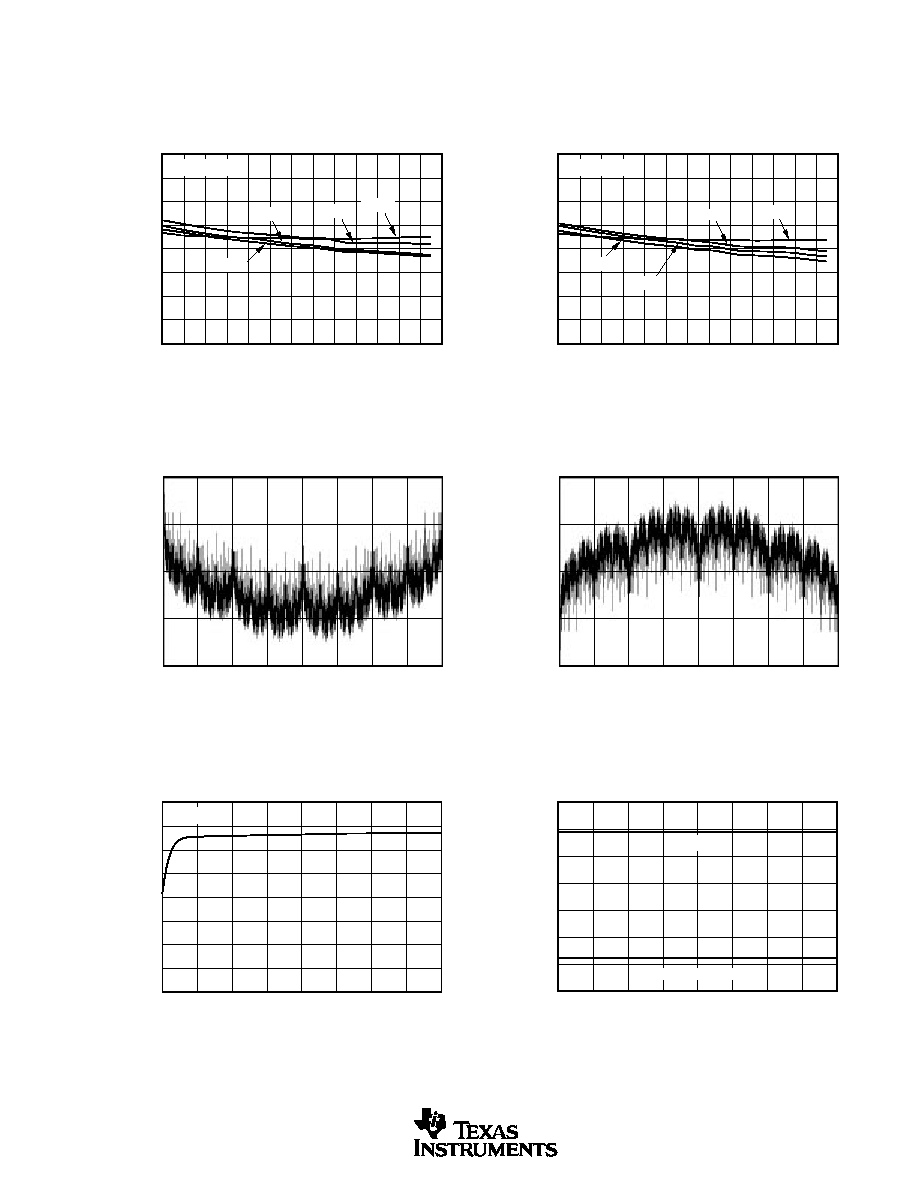
120
100
80
60
40
20
0
Frequency (Hz)
100
1k
10k
100k
1M
OUTPUT NOISE VOLTAGE vs FREQUENCY
Noise (nV/
Hz)
Code FFF
H
TYPICAL PERFORMANCE CURVES
At T
A
= +25
°
C, V
DD
= +3V, V
REFH
= +1.25V, and V
REFL
= 0V, representative unit, unless otherwise specified.
Time (100
µ
s/div)
WIDEBAND NOISE
(Bandwidth = 10kHz)
Noise Voltage (20
µ
V/div)

10
DAC7617
SBAS185
THEORY OF OPERATION
The DAC7617 is a quad, serial input, 12-bit, voltage output
DAC. The architecture is a classic R-2R ladder configuration
followed by an operational amplifier that serves as a buffer.
Each DAC has its own R-2R ladder network and output op
amp, but all share the reference voltage inputs. The minimum
voltage output ("zero-scale") and maximum voltage output
("full-scale") are set by external voltage references (V
REFL
and V
REFH
, respectively). The digital input is a 16-bit serial
word that contains the 12-bit DAC code and a 2-bit address
code that selects one of the four DACs (the two remaining
bits are unused). The converter can be powered from a single
+3V supply. Each device offers a reset function which imme-
diately sets all DAC output voltages and internal registers to
either zero-scale (code 000
H
) or mid-scale (code 800
H
). The
reset code is selected by the state of the RESETSEL pin
(LOW = 000
H
, HIGH = 800
H
). See Figure 1 for the basic
operation of the DAC7617.
ANALOG OUTPUTS
The output of the DAC7617 can swing to ground. Note that
the settling time of the output op amp will be longer with
voltages very near ground. Additionally, care must be taken
when measuring the zero-scale error. If the output amplifier
has a negative offset, the output voltage may not change for
the first few digital input codes (000
H
, 001
H
, 002
H
, etc.)
since the output voltage cannot swing below ground.
The behavior of the output amplifier can be critical in some
applications. Under short-circuit conditions (DAC output
shorted to V
DD
), the output amplifier can sink a great deal
more current than it can source. See the Specifications Table
for more details concerning short-circuit current.
FIGURE 1. Basic Single-Supply Operation of the DAC7617.
NOTE: (1) U package pin configuration shown. (2) As configured, RESET LOW sets all internal registers
to code 000
H
(0V). If RESETSEL is HIGH, RESET LOW sets all internal registers to code 800
H
(1.25V).
1
2
3
4
5
6
7
8
16
15
14
13
12
11
10
9
V
DD
V
OUTD
V
OUTC
V
REFL
V
REFH
V
OUTB
V
OUTA
AGND
RESETSEL
RESET
LOADREG
LDAC
CS
CLK
SDI
GND
Reset DACs
(2)
Update Selected Register
Update All DAC Registers
Chip Select
Clock
Serial Data In
DAC7617
(1)
0.1
µ
F
0.1
µ
F
0V to +1.25V
1
µ
F to 10
µ
F
+3V
+
0V to +1.25V
0V to +1.25V
0V to +1.25V
+1.25V
11
DAC7617
SBAS185
REFERENCE INPUTS
The minimum output of each DAC is equal to V
REFL
plus
a small offset voltage (essentially, the offset of the output
op amp). The maximum output is equal to V
REFH
1LSBplus
a similar offset voltage.
The current into the reference inputs depends on the DAC
output voltages and can vary from a few microamps to
approximately 0.4 milliamp. Bypassing the reference volt-
age or voltages with a 0.1
µ
F capacitor placed as close as
possible to the DAC7617 package is strongly recommended.
DIGITAL INTERFACE
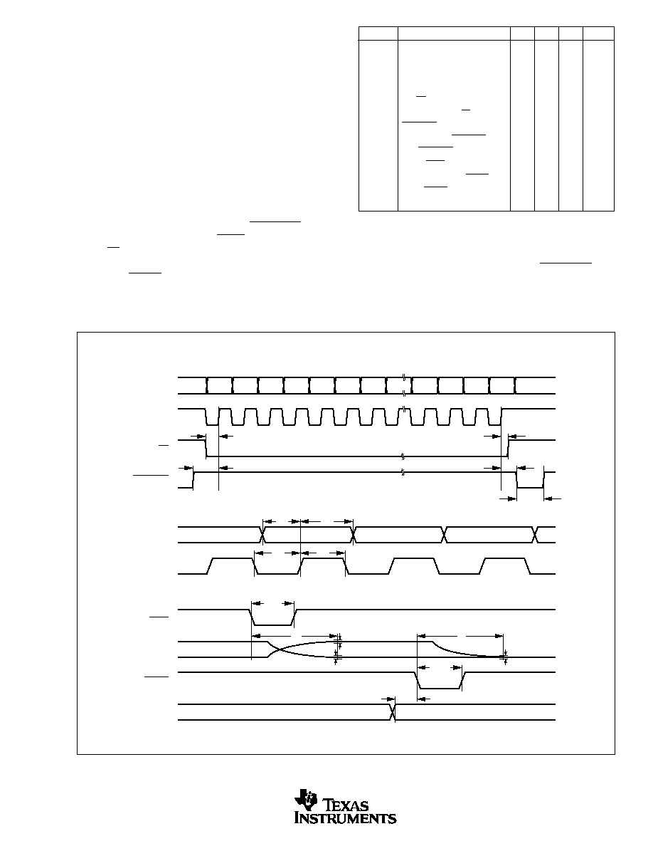
Figure 2 and Table I provide the basic timing for the
DAC7617. The interface consists of a serial clock (CLK),
serial data (SDI), a load register signal (LOADREG), and a
"load all DAC registers" signal (LDAC). In addition, a chip
select (CS) input is available to enable serial communication
when there are multiple serial devices. An asynchronous
reset input (RESET) is provided to simplify start-up condi-
tions, periodic resets, or emergency resets to a known state.
SYMBOL
DESCRIPTION
MIN
TYP
MAX
UNITS
t
DS
Data Valid to CLK Rising
25
ns
t
DH
Data Held Valid after CLK Rises
20
ns
t
CH
CLK HIGH
30
ns
t
CL
CLK LOW
50
ns
t
CSS
CS LOW to CLK Rising
55
ns
t
CSH
CLK HIGH to CS Rising
15
ns
t
LD1
LOADREG HIGH to CLK Rising
40
ns
t
LD2
CLK Rising to LOADREG LOW
15
ns
t
LDRW
LOADREG LOW Time
45
ns
t
LDDW
LDAC LOW Time
45
ns
t
RSSH
RESETSEL Valid to RESET LOW
25
ns
t
RSTW
RESET LOW Time
70
ns
t
S
Settling Time
10
µ
s
FIGURE 2. DAC7617 Timing.
The DAC code and address are provided via a 16-bit serial
interface, as shown in Figure 2. The first two bits select the
input register that will be updated when LOADREG goes
LOW (see Table II). The next two bits are not used. The last
12 bits are the DAC code which is provided, most significant
bit first.
TABLE I. Timing Specifications (T
A
= 40
°
C to +85
°
C).
A1
(MSB)
(LSB)
SDI
CLK
CS
LOADREG
A0
X
X
D11
D10
D9
D3
D2
D1
D0
SDI
CLK
LDAC
RESET
V
OUT
tcss
t
LD1
t
CL
t
CH
t
DS
t
DH
t
LD2
t
LDRW
t
LDDW
t
S
t
RSTW
t
RSSH
t
CSH
t
S
1 LSB
ERROR BAND
1 LSB
ERROR BAND
RESETSEL

12
DAC7617
SBAS185
If both CS and CLK are used, then CS should rise only when
CLK is HIGH. If not, then either CS or CLK can be used to
operate the shift register. See Table III for more information.
The digital data into the DAC7617 is double-buffered. This
allows new data to be entered for each DAC without disturb-
ing the analog outputs. When the new settings have been
entered into the device, all of the DAC outputs can be
updated simultaneously. The transfer from the input regis-
ters to the DAC registers is accomplished with a HIGH to
LOW transition on the LDAC input. It is possible to keep
this pin LOW and update each DAC via LOADREG be-
cause the DAC registers become transparent when LDAC is
LOW. However, as each new data word is entered into the
device, the corresponding output will update immediately
when LOADREG is taken LOW.
Digital Input Coding
The DAC7617 input data is in Straight Binary format. The
output voltage is given by the following equation:
where N is the digital input code (in decimal). This equation
does not include the effects of offset (zero-scale) or gain
(full-scale) errors.
STATE OF
SELECTED
SELECTED
STATE OF
INPUT
INPUT
ALL DAC
A1
A0
LOADREG
LDAC
RESET
REGISTER
REGISTER
REGISTERS
L
(1)
L
L
H
(2)
H
A
Transparent
Latched
L
H
L
H
H
B
Transparent
Latched
H
L
L
H
H
C
Transparent
Latched
H
H
L
H
H
D
Transparent
Latched
X
(3)
X
H
L
H
NONE
(All Latched)
Transparent
X
X
H
H
H
NONE
(All Latched)
Latched
X
X
X
X
L
ALL
Reset
(4)
Reset
(4)
NOTES: (1) L = Logic LOW. (2) H = Logic HIGH. (3) X = Don't Care. (4) Resets to either 000H or 800
H
, per the RESETSEL state (LOW = 000
H
, HIGH = 800
H
).
When RESET rises, all registers that are in their latched state retain the reset value.
CS
(1)
CLK
(1)
LOADREG
RESET
SERIAL SHIFT REGISTER
H
(2)
X
(3)
H
H
No Change
L
(4)
L
H
H
No Change
L
(5)
H
H
Advanced One Bit
L
H
H
Advanced One Bit
H
(6)
X
L
(7)
H
No Change
H
(6)
X
H
L
(8)
No Change
NOTES: (1) CS and CLK are interchangeable. (2) H = Logic HIGH. (3) X
= Don't Care. (4) L = Logic LOW (5) = Positive Logic Transition. (6) A HIGH
value is suggested in order to avoid a "false clock" from advancing the shift
register and changing the shift register. (7) If data is clocked into the serial
register while LOADREG is LOW, the selected input register will change
as the shift register bits "flow" through A1 and A0. This will corrupt the data
in each input register that has been erroneously selected. (8) RESET LOW
causes no change in the contents of the serial shift register.
TABLE II. Control Logic Truth Table.
TABLE III. Serial Shift Register Truth Table.
Note that CS and CLK are combined with an OR gate and
the output controls the serial-to-parallel shift register inter-
nal to the DAC7617 (see the block diagram on the front of
this data sheet). These two inputs are completely inter-
changeable. In addition, care must be taken with the state of
CLK when CS rises at the end of a serial transfer. If CLK is
LOW when CS rises, the OR gate will provide a rising edge
to the shift register, shifting the internal data one additional
bit. The result will be incorrect data and possible selection of
the wrong input register.
(V
REFH
V
REFL
) · N
4096
V
OUT
= V
REFL
+

13
DAC7617
SBAS185
LAYOUT
A precision analog component requires careful layout, ad-
equate bypassing, and clean, well-regulated power supplies.
As the DAC7617 offers single-supply operation, it will often
be used in close proximity with digital logic, microcontrollers,
microprocessors, and digital signal processors. The more
digital logic present in the design and the higher the switch-
ing speed, the more difficult it will be to keep digital noise
from appearing at the converter output.
Due to the DAC7617's single ground pin, all return currents,
including digital and analog return currents, must flow
through the GND pin. Ideally, GND would be connected
directly to an analog ground plane. This plane would be
separate from the ground connection for the digital compo-
nents until they were connected at the power entry point of
the system (see Figure 3).
The power applied to V
DD
should be well regulated and low
noise. Switching power supplies and DC/DC converters will
often have high-frequency glitches or spikes riding on the
output voltage. In addition, digital components can create
similar high-frequency spikes as their internal logic switches
states. This noise can easily couple into the DAC output
voltage through various paths between the power connec-
tions and analog output.
As with the GND connection, V
DD
should be connected to
a +3V power supply plane or trace that is separate from the
connection for digital logic until they are connected at the
power entry point. In addition, the 1
µ
F to 10
µ
F and 0.1
µ
F
capacitors shown in Figure 3 are strongly recommended. In
some situations, additional bypassing may be required, such
as a 100
µ
F electrolytic capacitor or even a
filter made up
of inductors and capacitors--all designed to essentially low-
pass filter the +3V supply, removing the high-frequency
noise (see Figure 3).
FIGURE 3. Suggested Power and Ground Connections for a DAC7617 Sharing a +3V Supply with a Digital System.
+3V
Power Supply
Optional
Digital Circuits
DAC7617
Other
Analog
Components
+3V
100
µ
F
1
µ
F to
10
µ
F
Ground
+3V
Ground
V
DD
AGND
0.1
µ
F
+
+

IMPORTANT NOTICE
Texas Instruments and its subsidiaries (TI) reserve the right to make changes to their products or to discontinue
any product or service without notice, and advise customers to obtain the latest version of relevant information
to verify, before placing orders, that information being relied on is current and complete. All products are sold
subject to the terms and conditions of sale supplied at the time of order acknowledgment, including those
pertaining to warranty, patent infringement, and limitation of liability.
TI warrants performance of its products to the specifications applicable at the time of sale in accordance with
TI's standard warranty. Testing and other quality control techniques are utilized to the extent TI deems necessary
to support this warranty. Specific testing of all parameters of each device is not necessarily performed, except
those mandated by government requirements.
Customers are responsible for their applications using TI components.
In order to minimize risks associated with the customer's applications, adequate design and operating
safeguards must be provided by the customer to minimize inherent or procedural hazards.
TI assumes no liability for applications assistance or customer product design. TI does not warrant or represent
that any license, either express or implied, is granted under any patent right, copyright, mask work right, or other
intellectual property right of TI covering or relating to any combination, machine, or process in which such
products or services might be or are used. TI's publication of information regarding any third party's products
or services does not constitute TI's approval, license, warranty or endorsement thereof.
Reproduction of information in TI data books or data sheets is permissible only if reproduction is without
alteration and is accompanied by all associated warranties, conditions, limitations and notices. Representation
or reproduction of this information with alteration voids all warranties provided for an associated TI product or
service, is an unfair and deceptive business practice, and TI is not responsible nor liable for any such use.
Resale of TI's products or services with
statements different from or beyond the parameters stated by TI for
that product or service voids all express and any implied warranties for the associated TI product or service,
is an unfair and deceptive business practice, and TI is not responsible nor liable for any such use.
Also see: Standard Terms and Conditions of Sale for Semiconductor Products. www.ti.com/sc/docs/stdterms.htm
Mailing Address:
Texas Instruments
Post Office Box 655303
Dallas, Texas 75265
Copyright
©
2001, Texas Instruments Incorporated