FLASH
FLASH
FLASH
FLASH
FLASH
AS8F512K32
Austin Semiconductor, Inc.
AS8F512K32
Rev. 5.0 5/03
Austin Semiconductor, Inc. reserves the right to change products or specifications without notice.
1
GENERAL DESCRIPTION
The Austin Semiconductor, Inc. AS8F512K32 is a 16 Megabit
CMOS FLASH Memory Module organized as 512Kx32 bits. The
AS8F512K32 achieves high speed access (70 to 150 ns), low power
consumption and high reliability by employing advanced CMOS memory
technology.
An on-chip state machine controls the program and erase func-
tions. The embedded byte-program and sector/chip erase functions are
fully automatic. Data-protection of any sector combination is accom-
plished using a hardware sector-protection feature.
The Erase/Resume function allows the sector erase operation to
read data from, or program to a non-erasing sector, then resume the
erase operation.
Device operations are selected by using standard commands into
the command register using standard microprocessor write timings. The
command register acts as an input to an internal state machine that
interprets the commands, controls the erase and programming opera-
tions, outputs the status of the device, and outputs data stored in the
device. On initial power-up operation, the device defaults to the read
mode.
FEATURES
�
Fast Access Times: 70, 90, 120 and 150ns
�
Operation with single 5V (�10%)
�
Theta JC= 1.00�
C
/w
�
User configurable as 512Kx32, 1Mx16, or 2Mx8
�
Eight Equal Sectors of 64K Bytes for each 512Kx8
�
Compatible with JEDEC EEPROM command set
�
Any Combination of Sectors can be Erased
�
Supports Full Chip Erase
�
Embedded Erase and Program Algorithms
�
TTL Compatible Inputs and CMOS Outputs
�
Built in decoupling caps for low noise operation
�
Suspend Erase/Resume Function
�
Individual Byte Read/ Write Control
�
10,000 Program/Erase Cycles
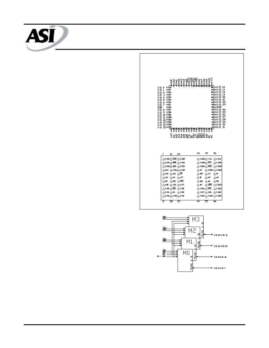
PIN ASSIGNMENT
(Top View)
AVAILABLE AS MILITARY
SPECIFICATIONS
�
SMD 5962-94612
�
MIL-STD-883
68 Lead CQFP (Q & Q1)
66 Lead PGA (P)
OPTIONS
MARKINGS
�
Timing
70ns
-70
90ns
-90
120ns
-120
150ns
-150
�
Package
Ceramic Quad Flat pack
Q
No. 702
Ceramic Quad Flatpack
Q1
Pin Grid Array
P
No. 904
For more products and information
please visit our web site at
www.austinsemiconductor.com
512K x 32 FLASH
FLASH MEMORY ARRAY

FLASH
FLASH
FLASH
FLASH
FLASH
AS8F512K32
Austin Semiconductor, Inc.
AS8F512K32
Rev. 5.0 5/03
Austin Semiconductor, Inc. reserves the right to change products or specifications without notice.
2
OPERATIONS
Read Mode
A low-level logic signal is applied to CE\ and OE\ pins to
read the output of the AS8F512K32. The CE\ is power control
and is used for device selection.
The delay from stable address to valid output data is the
address access time (tAVQA). The delay from CE\ equals logic
low and stable addresses to valid output data is the chip-en-
able access time (tELQV). The output-enable access time
(tGLQV) is the delay from OE\ =low logic to valid output data,
when CE\ =low logic and addresses are stable for at least tAVQA-
tGLQV.
Standby Mode
Icc supply current is reduced by applying a logic-high on
the CE\ to enter the standby mode. In the standby mode, the
outputs are placed in the high impedance state.
If the device is deselected during erasure or programming,
the device continues to draw active current until the operation
is complete.
Output Disable
OE\= VIL or CE\=VIH, output from the device is disabled
and the output pins (DQ0 - DQ7) are placed in the high-imped-
ance state.
Erasure and Programming
Erasure and programming of the AS8F512K32 are accom-
plished by writing a sequence of commands using standard
microprocessor write timings. The commands are written to a
command register and input to the command state machine.
The command state machine interprets the command entered
and initiates program, erase, suspend, and resume operations
as instructed. The command state machine acts as the inter-
face between the write-state machine and external chip opera-
tions. The write-state machine controls all voltage generation,
pulse generation, preconditioning and verification of the con-
tents of the memory. Program and block/chip-erase functions
are fully automatic. Once the end of a program or erase opera-
tion has been reached, the device internally resets to the read
mode. If Vcc drops below the low-voltage-detect level (VLKO),
any operation in progress is aborted and the device resets to
the read mode. If a byte-program or chip-erase operation is in
progress, additional program/erase operations are ignored un-
til the operation completes.
Command Definitions
Operating modes are selected by writing particular address
and data sequences into the command register Command Se-
quence Table . The device will reset to read mode if an incor-
rect address and data value or writing them in the incorrect
sequence transpires. The command register does not fill an
addressable memory location. The register is used to store the
command sequence, along with the address and data needed
by the memory array. Commands are written by setting CE\=VIL
and OE\= VIH and bring WE\ from logic-high to logic-low. Ad-
dresses are latched on the falling edge of WE\ and data is
latched on the rising edge of WE\. Holding WE\ =VIL and
toggling CE\ can be used as an alternative.
Read/Reset Command
The read/reset mode is activated by writing either of the
two read/reset command register. The device remains in this
mode until one of the other valid command sequences is input
into the command register. Memory data can be read with stan-
dard microprocessor read-cycle timing in the read mode.
On power up, the device defaults to the read/reset mode.
A read/reset command sequence if not required and memory
data is available.
Algorithm-Selection Command
The algorithm-selection command allows access to binary
code that matches the device with the proper programming -
and erase-command operations. After writing the three bus
cycle command sequence, the first byte of the algorithm-selec-
tion code (01) can be read from address XX00. The second
byte of the code (A4) can be read from address XX01. This
mode remains in effect until another valid command sequence
is written to the device.
Byte-Program Command
Byte-programming is a four-bus-cycle-command sequence.
The first three bus cycles put the device into the program-
setup state. The fourth bus cycle loads the address location
and the data to be programmed into the device. The addresses
are latched on the falling edge of WE\ and the data is latched
on the rising edge of WE\ in the fourth cycle. The raising edge
of WE\ starts the byte-program operation. The embedded
byte-programming function automatically provides needed
voltage and timing to program and verify the cell margin. Any
further commands written to the device during the program
operation are ignored.
Programming can be preformed at any address location in
any order. When erased, all bits are in a logic state 1. Logic 0s
are programmed into the device. Attempting to program logic 1
into a bit that has been previously programmed to logic 0 causes
the internal pulse counter to exceed the pulse-count limit. This
sets the exceed-timing-limit indicator (DQ5) to a logic high state.
Only an erase operation can change bits from logic 0 to logic 1.
The status of the device during the automatic program-
ming operation can be monitored for the completion using the
data-polling feature or the toggle-bit feature . See the "opera-
tion status" for the full description.

FLASH
FLASH
FLASH
FLASH
FLASH
AS8F512K32
Austin Semiconductor, Inc.
AS8F512K32
Rev. 5.0 5/03
Austin Semiconductor, Inc. reserves the right to change products or specifications without notice.
3
Chip Erase Command
Chip-erase is a six-bus-cycle command sequence. The first
three bus cycles put the device into the erase-setup state. The
next two bus cycles unlock the erase mode. The sixth bus cycle
loads the chip erase command. This command sequence is
required to ensure that the memory contents are not erased
accidentally. The rising edge of WE\ starts the chip erase op-
eration. Any further commands written to the device during
the chip erase operation is ignored.
The embedded chip erase function automatically provides
voltage and timings needed to program and verify all the memory
cells prior to electrical erase. It then erases and verifies the cell
margin automatically. The user is not required to program the
memory cells prior to erase. The status of the device during the
automatic chip erase operation can be monitored for comple-
tion using the data-polling feature. See the "operation status"
section for a full description.
Sector-Erase Command
Sector erase is a six-bus-cycle command sequence. The
first three bus cycles put the device into the erase-setup state.
The next two bus cycles unlock the erase mode. The sixth bus
cycle loads the sector erase command and the sector address
location to be erased. Any address location within the desired
sector can be used. The addresses are latched on the falling
edge of WE\ in the sixth bus cycle. After a delay of 100-ms
from the rising edge of WE\, the sector erase operation begins
in the selected source.
Sectors can be selected to be erased concurrently during
the sector-erase command sequence. For each additional sec-
tor selected for erase, another bus cycle is issued. The bus
cycle loads the next sector-address location and the sector-
erase command. The time between the end of the previous bus
cycle and the start of the next bus cycle must be less than 100
ms-other wise, the new sector location is not loaded. A time
delay of 100 ms from the raising edge of the last WE\ starts the
sector erase operation. If there is a falling edge of WE\ within
the 100 ms time delay, the timer is reset.
One to eight sector address locations can be loaded in any
order. The state of the delay timer can be monitored using the
sector-erase-delay indicator (DQ3). If DQ3 is logic low, the time
delay has not expired. See the "operation status" for the full
description.
Any commands other than erase-suspend (B0) or sector
erase (30) written to the device during the sector erase opera-
tion causes the device to exit the sector erase mode. The con-
tents of the sector(s) selected for erase is not valid. To com-
plete the sector-erase operation, reissue the sector erase com-
mand.
The embedded sector erase function automatically
provides voltage and timings needed to program and verify all
the memory cells prior to electrical erase and then erases and
verifies the cell margin automatically. The user is not required
to program the memory cells prior to erase. The status of the
device during the automatic sector erase operation can be moni-
tored for completion using the data-polling feature or the toggle
bit feature. See the "operation status" section for a full de-
scription.
Erase-Suspend Command
Sector-erase operations may be interrupted by the erase-
suspend command (B0) , in order to read data from an unaltered
sectors of the device. Erase-suspend is a one-bus-cycle com-
mand. The addresses can be VIL or VIH and the erase-suspend
command (B0) is latched on the rising edge of WE\. Once the
sector-erase operation is in progress, the erase-suspend com-
mand request the internal write-state-machine to halt operation
at predetermined break points. The erase-suspend command is
valid only during the sector-erase operation and is valid only
during the byte-programming and chip-erase operations. The
sector-erase delay timer expires immediately if the erase-sus-
pend command is issued while the delay is active.
After erase-suspend is issued, the device takes between
0.1ms and 15 ms to suspend the operation. The toggle bit must
be monitored to determine when the suspend has been ex-
ecuted. When the toggle bit stops toggling, data can be read
from sectors that are not selected for erase. See the "operation
status" section for a full definition. Reading from a sector
marked for erase can result in invalid data.
Once the sector-erase operation is suspended, further
writes of the erase-suspend command are ignored. Any com-
mand other than erase-suspend (B0) or erase-resume (30H)
written to the device during the erase-suspend mode causes
the device to exit the suspend mode. To complete the sector-
erase operation, reissue the sector-erase command sequence.
Erase-Resume Command
The erase-resume command (30H) restarts a suspended
sector erase operation from where it was halted to completion.
Erase-resume is a one-bus-cycle command. The addresses can
be VIL or VIH and the erase-resume command (30H) is latched
on the rising edge of WE\. When an erase-suspend/ erase-
resume command combination is written, the internal pulse
counter (exceed timing limit) is reset. The erase-resume com-
mand is valid only in the erase-suspend state. After the erase-
resume command is executed, the device returns to the valid
sector-erase state and further writes of the erase-resume com-
mands are ignored. After the device has resumed the sector-
erase operation, another erase-resume command can be issued
to the device.

FLASH
FLASH
FLASH
FLASH
FLASH
AS8F512K32
Austin Semiconductor, Inc.
AS8F512K32
Rev. 5.0 5/03
Austin Semiconductor, Inc. reserves the right to change products or specifications without notice.
4
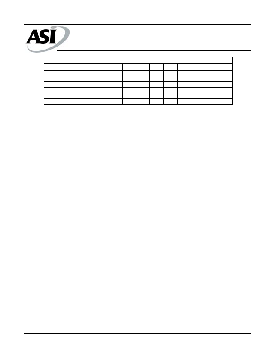
OPERATION STATUS
NOTES:
1. T= toggle, D=data, X=data undefined
2. DQ4, DQ2, DQ1, DQ0 are reserved for future use.
Status Bit Definition
During operation of the automatic embedded program and
erase functions, the status of the device can be determined by
reading the data state of designated outputs. The data-polling
bit (DQ7) and toggle-bit (DQ6) require multiple successive reads
to observe a change in the state of the designated output.
Operation Status Flags Table defines the values of the Flag
status.
Data-Polling DQ7
The data-polling status outputs the complement of the data
latched into the DQ7 data register while the write-state machine
is engaged in a program or erase operation. Data bit DQ7 chang-
ing from complement to true indicates the end of an operation.
Data-polling is available only during the byte-programming,
chip-erase, sector-erase, and sector-erase timing delay. Data-
polling is valid after the rising edge of ?W/E in the last bus cycle
of the command sequence loaded into the command register.
During a byte-program operation, reading DQ7 outputs
the complement of the DQ7 data to be programmed at the se-
lected address location. Upon completion, reading DQ7 out-
puts the true DQ7 data loaded into the program data register.
During the erase operations, reading DQ7 outputs a 0. Upon
completion, reading DQ7 outputs a 1. Also, data polling must
be performed at a new sector address that is within a sector
being erased; otherwise the status is not valid. When using
data-polling, the address should remain stable throughout the
operation.
During a data-polling read, while ?W/E is low, data bit DQ7
can change asynchronously. Depending on the read timing,
the system can read valid data on DQ7, while other DQ pins are
still invalid. A subsequent read of the device is valid.
Data-Polling DQ6
The function of toggle-bit status, is to output data on
DQ6 that toggles between 1 and 0 while the write-state ma-
chine is engaged in a program or erase operation. When toggle-
bit DQ6 stops toggling after two consecutive reads to the same
address, the operation is complete. The toggle-bit is only
available during the byte-programming, chip-erase, and sector-
erase timing delay. Toggle-bit data is valid after the raising
edge of ?W/E in the last bus cycle of the command sequence
loaded into the command register. Depending on the read tim-
ing, DQ6 can stop toggling while other DQ pins are still invalid.
A subsequent read of the device is valid.
Exceed Time Limit DQ5
The program and erase operations use an internal pulse
counter to limit the number of pulses applied. If the pulse count
limit is exceeded, DQ5 is set to a 1 data state. This indicates that
the program or erase operation has failed. DQ7 will not change
from complemented data to true data and DQ6 will not stop
toggling when read. To continue operation, the device must be
reset.
This condition occurs when attempting to program a logic
1 state into a bit that has been programmed previously to a
logic 0. Only an erase operation can change bits from 0 to 1.
After reset, the device is functional and can be erased and
reprogrammed.
Sector-Load- Timer DQ3
DQ3 is the sector-load timer status bit it determines if the
time to load additional sector addresses has expired. DQ3 re-
mains a logic low for 80
�s after completion of a sector-erase
sequence. This indicates another sector-erase command se-
quence can be issued. If DQ3 is at logic high, it indicates that
the delay has expired and attempts to issue additional sector-
erase commands are ignored.
The data polling bit and toggle bit are valid during the 100
�s time delay and can be used to determine if a valid sector
erase command has been issued. To ensure additional sector
erase commands have been accepted, the status of DQ3 should
be read before and after each additional sector-erase command.
If DQ3 is at a logic low on both reads, then the additional sec-
tor-erase was accepted.
Device Operations
2
DQ7
DQ6
DQ5
DQ4
DQ3
DQ2
DQ1
DQ0
Byte-programming in progress
D\
T
0
X
0
X
X
X
Byte-programming exceed time limit
D\
T
1
X
0
X
X
X
Byte-programming complete
D
D
D
D
D
D
D
D
Sector/chip erase in progress
0
T
0
X
1
X
X
X
Sector/chip erase exceed time limit
0
T
1
X
1
X
X
X
Sector/chip erase complete
1
1
1
1
1
1
1
1
Operation Status Flags
1
Table

FLASH
FLASH
FLASH
FLASH
FLASH
AS8F512K32
Austin Semiconductor, Inc.
AS8F512K32
Rev. 5.0 5/03
Austin Semiconductor, Inc. reserves the right to change products or specifications without notice.
5
DATA PROTECTION
Hardware-Sector Protection Feature
This feature disables both programming and erase opera-
tions on any combination of one to eight sectors. Commands
to program or erase a protected sector do not change the data
contained in the sector. The data-polling and toggle bits oper-
ate for 2ms to 100ms and then return to valid data. This feature
is enabled using high-voltage V
ID
(11.5V to 12V) on address
pin A9 and control pin OE\ and V
IL
on control pin CE\.
The device is delivered with all sector unprotected.
Sector-unprotected mode is available to unprotect protected
sectors.
Sector Protect Operation
The sector protect mode is activated when WE\=V
IH
,
CE\=V
IL
,
and address pin A9 and control pin OE\ are forced to
V
ID
. The sector-select address pins A18, A17, and A16 are
used to select the sector to be protected. Address pins A0-A15
and I/O pins DQ0- DQ7 must be stable and can be V
IL
or V
IH
.
Once the addresses are stable, WE\ is pulsed low for 100 ms.
The operation begins on the falling edge of WE\ and terminates
on the raising edge of WE\.
Sector Protect Verify
Verification of sector protection is activated when
WE\=V
IH
, CE\=V
IL
, OE\=V
IL
, and address pin A9 is V
ID
.
Address pins A0 and A6 are set to V
IL
, and A1 is set to V
IH
.
The sector address pins A18, A17, and A16 select the sector to
be verified. The other addresses can be V
IH
or V
IL
. If the
sector selected if protected, the DQs output O1. If the sector
selected is unprotected the DQs output is 00.
Sector protection can also be verified using the algorithm-
selection command. After issuing the three bus-cycle command
sequence, the sector protection status can be read on DQ0. Set
address pins A0 = V
IL
, A1 = V
IH
, and A6 = V
IL
. Sector
address pins A18, A17, and A16 select the sector to be verified.
The remaining addresses are set to V
IL
. If the sector selected is
protected. DQ0 outputs a 1 state, and if the sector selected is
unprotected DQ0 outputs a 0 state. This mode remains in effect
until another valid sequence is written to the device.
Sector Unprotect
Prior to sector unprotected, all sectors should be protected
using the sector unprotect mode. The sector unprotect is acti-
vated when WE\=V
IH
, and control pin CE\, OE\, and address
pin A9 are forced to V
ID
. Address pins A6, A12, and A16 are
set to V
IH
. The sector select address pins A18, A17, and A16
can be V
IL
or V
IH
. All eight sectors are unprotected in parallel.
Once the inputs are stable, WE\ is pulsed low for 10ms. The
unprotect operation begins on the falling edge of WE\ and
terminates on the raising edge of WE\.
Sector Unprotect Verify
Verification of the sector unprotected is activated when
WE\ = V
IH
, OE\ = V
IL
, CE\ = V
IL
, and address pin A9 = V
ID
.
Select the sector to be verified. Address A1 and A6 are set to
V
IH
and A0 to V
IL
. The other addresses can be V
IL
or V
IH
. If
the sector selected is protected, the DQs output a 01, if sector
selected is unprotected the DQs output a 00. Sector unprotect
can also be read using the algorithm selection command.
Low VCC Write Lock Out
During power-up and power-down , are locked out for V
CC
less than VLKO If V
CC
<VLKO, the command inputs is dis-
abled and the device is reset to the read mode. On power-up, if
CE\=V
IL
, WE\= V
IL
, and OE\=V
IH
, the device does not accept
commands on the raising edge of WE. The device automati-
cally powers up in the read mode.
Glitiching
Pulses of less than 5ns (typical) on WE\, OE\, and CE\ will
not issue a write cycle.
Power Supply Consideration
Each device should have as a maximum of 0.1 mF ceramic
capacitor connected between Vcc and Vss to suppress circuit
noise. Printed circuit traces to Vcc should have be appropriate
to handle the current demand and minimize inductance.


