
SDRAM
SDRAM
SDRAM
SDRAM
SDRAM
AS4SD16M16
Austin Semiconductor, Inc.
AS4SD16M16
Rev. 1.0 11/02
Austin Semiconductor, Inc. reserves the right to change products or specifications without notice.
1
FEATURES
· Full Military temp (-55°C to 125°C) processing available
· Configuration: 16 Meg x 16 (4 Meg x 16 x 4 banks)
· Fully synchronous; all signals registered on positive
edge of system clock
· Internal pipelined operation; column address can be
changed every clock cycle
· Internal banks for hiding row access/precharge
· Programmable burst lengths: 1, 2, 4, 8 or full page
· Auto Precharge, includes CONCURRENT AUTO
PRECHARGE and Auto Refresh Modes
· Self Refresh Mode (IT)
· 64ms, 8,192-cycle refresh (IT)
· <24ms 8,192 cycle recfresh (XT)
· WRITE Recovery (t
WR
= "2 CLK")
· LVTTL-compatible inputs and outputs
· Single +3.3V ±0.3V power supply
OPTIONS
MARKING
· Plastic Package - OCPL*
54-pin TSOP (400 mil) DG No. 901
·
Timing (Cycle Time)
7.5ns @ CL = 3 (PC133) or
-75
7.5ns @ CL = 2 (PC100)
·
Operating Temperature Ranges
-Industrial Temp (-40°C to 85° C) IT
-Industrial Plus Temp
(-45°C to +105°C)
IT+
-Military Temp (-55°C to 125°C) XT***
*Off-center parting line
**CL = CAS (READ) latency
***Consult Factory
PIN ASSIGNMENT
(Top View)
54-Pin TSOP
Note: "\" indicates an active low.
256 MB: 16 Meg x 16 SDRAM
Synchronous DRAM Memory
For more products and information
please visit our web site at
www.austinsemiconductor.com
KEY TIMING PARAMETERS
SPEED
CLOCK
SETUP
HOLD
GRADE
FREQUENCY CL = 2** CL = 3**
TIME
TIME
-75
133 MHz
5.4ns
1.5ns
0.8ns
-75
100 MHz
6ns
1.5ns
0.8ns
ACCESS TIME
Configuration
4 Meg x 16 x 4 banks
Refresh Count
8K
Row Addressing
8K (A0-A12)
Bank Addressing
4 (BA0, BA1)
Column Addressing
512 (A0-A8)
16 Meg x 16

SDRAM
SDRAM
SDRAM
SDRAM
SDRAM
AS4SD16M16
Austin Semiconductor, Inc.
AS4SD16M16
Rev. 1.0 11/02
Austin Semiconductor, Inc. reserves the right to change products or specifications without notice.
2
GENERAL DESCRIPTION
The 256MB SDRAM is a high-speed CMOS, dynamic ran-
dom-access memory containing 268,435,456 bits. It is internally
configured as a quad-bank DRAM with a synchronous inter-
face (all signals are registered on the positive edge of the clock
signal, CLK). Each of the 67,108,864-bit banks is organized as
8,192 rows by 512 columns by 16 bits.
Read and write accesses to the SDRAM are burst oriented;
accesses start at a selected location and continue for a pro-
grammed number of locations in a programmed sequence. Ac-
cesses begin with the registration of an ACTIVE command,
which is then followed by a READ or WRITE command. The
address bits registered coincident with the ACTIVE command
are used to select the bank and row to be accessed (BA0, BA1
select the bank; A0-A12 select the row). The address bits
registered coincident with the READ or WRITE command are
used to select the starting column location for the burst access.
The SDRAM provides for programmable READ or WRITE
burst lengths of 1, 2, 4, or 8 locations, or the full page, with a
burst terminate option. An auto precharge function may be
enabled to provide a self-timed row precharge that is initiated at
the end of the burst sequence.
The 256MB SDRAM uses an internal pipelined architec-
ture to achieve high-speed operation. This architecture is com-
patible with the 2n rule of prefetch architectures, but it also
allows the column address to be changed on every clock cycle
to achieve a high-speed, fully random operation. Precharging
one bank while accessing one of the other three banks will hide
the precharge cycles and provide seamless, high-speed, ran-
dom-access operation.
The 256Mb SDRAM is designed to operate in 3.3V memory
systems. An auto refresh mode is provided, along with a power-
saving, power-down mode. All inputs and outputs are LVTTL-
compatible.
SDRAMs offer substantial advances in DRAM operating
performance, including the ability to synchronously burst data
at a high data rate with automatic column-address generation,
the ability to interleave between internal banks to hide precharge
time and the capability to randomly change column addresses
on each clock cycle during a burst access.
FUNCTIONAL BLOCK DIAGRAM
SDRAM
SDRAM
SDRAM
SDRAM
SDRAM
AS4SD16M16
Austin Semiconductor, Inc.
AS4SD16M16
Rev. 1.0 11/02
Austin Semiconductor, Inc. reserves the right to change products or specifications without notice.
3
PIN NUMBER
SYMBOL
TYPE
DESCRIPTION
38
CLK
Input
Clock: CLK is driven by the system clock. All SDRAM input
signals are sampled on the positive edge of CLK. CLK also
increments the internal burst counter and controls the output
registers.
37
CKE
Input
Clock Enable: CKE activates (HIGH) and deactivates (LOW) the
CLK signal. Deactivating the clock provides PRECHARGE
POWER-DOWN and SLEF REFRESH operation (all banks idle),
ACTIVE POWER-DOWN (row active in any bank) or CLOCK
SUSPEND operation (burst/access in progress). CKE is
synchronous except after the device enters power-down and self
refresh modes, where CKE becomes asynchronous until after
exiting the same mode. The input buffers, including CLK, are
disabled during power-down and self refresh modes, providing low
standby power. CKE may be tied HIGH.
19
CS\
Input
Chip Select: CS\ enables (registered LOW) and disables
(registered HIGH) the command decoder. All commands are
masked when CS\ is registered HIGH. CS\ provides for external
bank selection on systems with multiple banks. CS\ in considered
part of the command code.
16, 17, 18
WE\, CAS\,
RAS\
Input
Command Inputs: WE\, CAS\ and RAS\ (along with CS\) define
the command being entered.
15, 39
DQML, DQMU
Input
Input/Output Mask: DQM is an input mask signal for write
accesses and an output enable signal for read accesses. Input
data is masked when DWM is sampled HIGH during a WRITE
cycle. The outptu buffers are placed in a High-Z state (two-clock
latency) when DQM is sampled HIGH during a READ cycle.
DQML corresponds to DQ0-DQ7 and DQMH corresponds to
DQ8-DQ15. DQML and DQMH are considered same state when
referenced as DQM.
20, 21
BA0, BA1
Input
Bank Address Inputs: BA0 and BA1 define to which bank the
ACTIVE, READ, WRITE, or PRECHARGE command is being
applied.
23-26, 29-34, 22, 35, 36
A0 - A12
Input
Address Inputs: A0-A12 are sampled during the ACTIVE
command (row address A0-A12) and READ/WRITE command
(column-address A0-A8; with A10 defining auto precharge) to
select one location out of the memory array in the respective
bank. A10 is sampled during a PRECHARGE command to
determine if all banks are to be prechaged (A10 [HIGH]) or bank
selected by (A10 [LOW]). The address inputs also provide the
op-code during LOAD MODE REGISTER COMMAND.
2, 4, 5, 7, 8, 10, 11, 13, 42,
44, 45, 47, 48, 50, 51, 53
DQ0 - DQ15
I/O
Data Input/Output: Data bus
40
NC
---
No Connect: This pin should be left unconnected.
3, 9, 43, 49
V
DD
Q
Supply
DQ Power: Isolated DQ power to the die for improved noise
immunity.
6, 12, 46, 52
V
SS
Q
Supply
DQ Ground: Isolated DQ ground to the die for imporved noise
immunity.
1, 14, 27
V
DD
Supply Power Supply: +3.3V ±0.3V
28, 41, 54
V
SS
Supply Ground
PIN DESCRIPTIONS

SDRAM
SDRAM
SDRAM
SDRAM
SDRAM
AS4SD16M16
Austin Semiconductor, Inc.
AS4SD16M16
Rev. 1.0 11/02
Austin Semiconductor, Inc. reserves the right to change products or specifications without notice.
4
FUNCTIONAL DESCRIPTION
In general, the 256MB SDRAMs are quad-bank DRAMs
that operate at 3.3V and include a synchronous interface (all
signals are registered on the positive edge of the clock signal,
CLK). Each of the 67,108,864-bit banks is organized as 8,192
rows by 512 columns by 16 bits.
Read and write accesses to the SDRAM are burst oriented;
accesses start at a selected location and continue for a
programmed number of locations in a programmed sequence.
Accesses begin with the registration of an ACTIVE command,
which is then followed by a READ or WRITE command. The
address bits registered coincident with the ACTIVE command
are used to select the bank and row to be accessed (BA0 and
BA1 select the bank, A0 - A12 select the row). The address bits
(A0 - A8) registered coincident with the READ or WRITE
command are used to select the starting column location for the
burst access.
Prior to normal operation, the SDRAM must be initialized.
The following sections provide detailed information covering
device initialization, register definition, command descriptions
and device operation.
Initialization
SDRAMs must be powered up and initialized in a predefined
manner. Operational procedures other than those specified
may result in undefined operation. Once power is applied to
VDD and VDDQ (simultaneously) and the clock is stable (stable
clock is defined as a signal cycling within timing constraints
specified for the clock pin), the SDRAM requires a 100µs delay
prior to issuing any command other than a COMMAND
INHIBIT or NOP. Starting at some point during this 100µs
period and continuing at least through the end of this period,
COMMAND INHIBIT or NOP commands should be applied.
Once the 100µs delay has been satisfied with at least one
COMMAND INHIBIT or NOP command having been applied,
a PRECHARGE command should be applied. All banks must
then be precharged, thereby placing the device in the all banks
idle state.
Once in the idle state, two AUTO REFRESH cycles must
be preformed. After the AUTO REFRESH cycles are complete,
the SDRAM is ready for mode register programming. Because
the mode register will power up in an unknown state, it should
be loaded prior to applying any operational command.
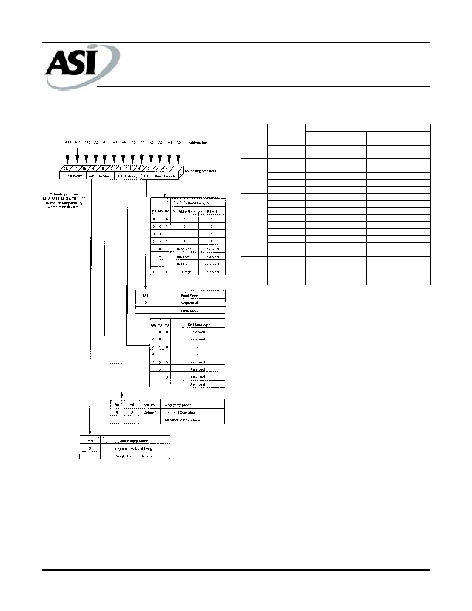
Register Definition
MODE REGISTER
The mode register is used to define the specific mode of
operation of the SDRAM. This definition includes the
selection of a burst length, a burst type, a CAS latency, an
operating mode and a write burst mode, as shown in Figure 1.
The mode register is programmed via the LOAD MODE
REGISTER command and will retain the stored information until
it is programmed again or the device loses power.
Mode register bits M0 - M2 specify the burst length, M3
specifies the type of burst (sequential or interleaved), M4 - M6
specify the CAS latency, M7 and M8 specify the operating
mode, M9 specifies the write burst mode, and M10 and M11 are
reserved for future use. Address A12 (M12) is undefined but
should be driven LOW during loading of the mode register.
The mode register must be loaded when all banks are idle,
and the controller must wait the specified time before initiating
the subsequent operation. Violating either of these require-
ments will result in unspecified operation.
Burst Length
Read and write accesses to the SDRAM are burst oriented,
with the burst length being programmable, as shown in Figure
1. The burst length determines the maximum number of column
locations that can be accessed for a given READ or WRITE
command. Burst lengths of 1, 2, 4, or 8 locations are available
for both the sequential and the interleaved burst types, and a
full-page burst is available for the sequential types. The full-
page burst is used in conjunction with the BURST TERMI-
NATE command to generate arbitrary burst lengths.
Reserved states should not be used as unknown opera-
tion or incompatibility with future versions may result.
When a READ or WRITE command is issued, a block of
columns equal to the burst length is effectively selected. All
accesses for that burst take place within this block, meaning
that the burst will wrap within the block if a boundary is reached.
The clock is uniquely selected by A1-A8 when the burst length
is set to two; by A2-A8 when the burst length is set to four, and
by A3-A8 when the burst length is set to eight. The remaining
(least significant) address bit(s) is (are) used to select the start-
ing location within the block. Full-page bursts wrap within the
page if the boundary is reached.
Burst Type
Accesses within a given burst may be programmed to be
either sequential or interleaved; this is referred to as the burst
type and is selected via bit M3.
The ordering of accesses within a burst is determined by
the burst length, the burst type and the starting column ad-
dress, shown in table 1.
SDRAM
SDRAM
SDRAM
SDRAM
SDRAM
AS4SD16M16
Austin Semiconductor, Inc.
AS4SD16M16
Rev. 1.0 11/02
Austin Semiconductor, Inc. reserves the right to change products or specifications without notice.
5
FIGURE 1: Mode Register Definition TABLE 1: Burst Definition
TYPE = SEQUENTIAL TYPE = INTERLEAVED
A0
0
0-1
0-1
1
1-0
1-0
A1 A0
0 0
0-1-2-3
0-1-2-3
0 1
1-2-3-0
1-0-3-2
1 0
2-3-0-1
2-3-0-1
1 1
3-0-1-2
3-2-1-0
A2 A1 A0
0 0 0
0-1-2-3-4-5-6-7
0-1-2-3-4-5-6-7
0 0 1
1-2-3-4-5-6-7-0
1-0-3-2-5-4-7-6
0 1 0
2-3-4-5-6-7-0-1-
2-3-0-1-6-7-4-5
0 1 1
3-4-5-6-7-0-1-2
3-2-1-0-7-6-5-4
1 0 0
4-5-6-7-0-1-2-3
4-5-6-7-0-1-2-3
1 0 1
5-6-7-0-1-2-3-4
5-4-7-6-1-0-3-2
1 1 0
6-7-0-1-2-3-4-5
6-7-4-5-2-3-0-1
1 1 1
7-0-1-2-3-4-5-6
7-6-5-4-3-2-1-0
Full
Page
(y)
n=A0-A8
(location 0-y)
Cn, Cn+1, Cn+2, Cn+3,
Cn+4...
...Cn-1,
Cn...
Not Supported
4
8
BURST
LENGTH
STARTING
COLUMN
ORDER OF ACCESSES WITHIN A BURST
2
NOTES:
1. For full-page access: y=512
2. For a burst length of two, A1-A8 select the block-of-two burst;
A0 selects the starting column within the block.
3. For a burst length of four, A2-A8 select the block-of-four burst;
A0-A1 selects the starting column within the block.
4. For a burst length of eight, A3-A8 select the block-of-eight burst;
A0-A2 selects the starting column within the block.
5. For a full-page burst, the full row is selected and A0-A8 select the
starting column.
6. Whenever a boundary of the block is reached within a given
sequence above, the following access wraps within the block.
7. For a burst length of one, A0-A8 select the unique column to be
accessed, and mode register bit M3 is ignored.