
KSI-W012-001
1
SL5001P/2P
TONE RINGER
Description
The oscillator frequencies can be adjusted over a wide range by selection of external
components
Features
· Designed telephone bell replacement
· Adjustable 2-frequency tone
· Low current drain
· Built-in hysteresis prevents false triggering and rotary dial "Chirp"
· External triggering ringer disable(5001P)
· Adjustable for reduced supply initiation current(5002P)
Applications
· Telephone tone ringers
· Alarms or other alerting devices
· Extension tone ringer modules
Ordering
Information
Type NO.
Marking
Package Code
SL5001P SL5001
DIP8
SL5002P SL5002
DIP8
Outline Dimensions unit :
mm
S
S
e
e
m
m
i
i
c
c
o
o
n
n
d
d
u
u
c
c
t
t
o
o
r
r

KSI-W012-001
2
Absolute Maximum Ratings
(Ta = 25
°C)
Characteristic Symbol
Rating
Unit
Supply Voltage
V
CC
30 V
Power Dissipation
P
D
400
mW
Operating Temperature
T
opr
-45+65
°C
Storage Temperature
T
stg
-65+150
°C
Block Diagram
Electrical Characteristics
(Unless otherwise specified, Ta = 25
°C)
Characteristic Symbol
Test
Condition
Min.
Typ.
Max.
Unit
Operating Supply Voltage
V
CC
- -
-
29
V
Initiation Supply Voltage
V
CC(INI)
Trigger-In Open,
No Load
17 19 21 V
Sustaining Voltage
V
SUS
Trigger-In Open,
No Load
9.7 11 13 V
Initiation Supply Current
I
CC(INI)
R
SL
= 6.8K(5002P)
0.8 2.5 4.2 mA
Sustaining Current
I
SUS
V
CC
=V
SUS
, No Load
0.7
1.2
-
mA
Trigger Voltage
V
TR
5001P
10.5
11 - V
Trigger Current
I
TR
5001P
10 20
1000 µA
Disable Voltage
V
DIS
5001P
- 0.4 0.8 V
Disable Current
I
DIS
5001P
-40 -50 - µA
Output Voltage
V
OUT
V
CC
=21V, No Load
17
19
21
V
Oscillator Frequency Tolerance
f
O
- -
-
±7
%
SL5001P/2P
8
1
2
3
4
5
6
7
R E G ULA T O R W I T H
HY S T E R E S I S
A M P
HF O
LF O
O S C1
I n p u t
O S C1
O u t p u t
O S C 2
I n p u t
O S C2
O u t p u t
G ND
O u t p u t
T r i g g e r -I n
LF O : Lo w F r e q u e n c y O S C.
HF O : Hi g h F r e q u e n c y O S C.
P i n 3,4 : Lo w F r e q u e n c y T i me Co n s t a n t
P i n 6,7 : Hi g h F r e q u e n c y T i me Co n s t a n t
* R e g u l a t o r c i r c u i t h a s b u i l t -i n h y s t e r e s i s t o p r e v e n t f a l s e
t r i g g e r i n g a n d r o t a r y d i a l "Ch i r p s "
V
CC

KSI-W012-001
3
Electrical Characteristics (continued)
1.Initiation supply voltage V
CC(INI)
must be exceeded to trigger oscillation.
2.Sustaining voltage (V
SUS
) is the supply voltage required to maintain oscillation.
3.Trigger voltage (V
TR
) and trigger current(I
TR
) are the conditions applied to trigger in to
start oscillation for V
SUS
V
CC
V
CC(INI)
.
4.Disable voltage (V
DIS
) and disable current(I
DIS
) are the conditions applied to trigger in
to inhibit oscillation for V
CC(INI)
< V
CC
5.Trigger current must be limited to this value externally.
6.Oscillator frequencies are given by equations :
· f
L
= 1/(1.234RC) where R is the resistance connected between pins 3 and 4, and C is
the capacitance connected between pin 3 and ground.
· f
H1
= 1/(1.515RC) where R is the resistance connected between pins 6 and 7, and C is
capacitance connected between pin 6 and ground.
Norminal rate (f
HA
) is the HFO when the output of LFO is high
· f
H2
= 1.25f
H1
, higher rate(f
H2
) is the HFO when the output of LFO is low.
Typical Performance Characteristics
SL5001P/2P
I c c - V c c
S u p p l y V o l t a g e V c c (V )
S
u
p
p
l
y
C
u
r
r
ent
I
c
c
(m
A
)
2
6
10
14 18
22 26
30 34
0.5
1.0
1.5
2.0
2.5
3.0
3.5
No Lo a d
5001
Lo a d C u r r e n t I
L
(mA r ms )
Lo
a
d
V
o
l
t
a
g
e
V
L
(
Vr
m
s
)
V
L
- I
L
0
10
30
40
20
2
4
6
8
10
V c c =21V
V c c =15V
5001
I c c - V c c
S u p p l y V o l t a g e V c c (V )
S
u
p
p
l
y
C
u
r
r
en
t
I
c
c
(mA
)
0.5
1.0
1.5
2.0
2.5
3.0
3.5
4.0
2
6
10 14 18 22 26 30 34
5002
A :R
S L
< 6.8K
B:R
S L
= 6.8K
C :R
S L
> 6.8K
I c c
( I N I )
- R
S L
R e s i s t a n c e R
S L
(K)
S
u
p
p
l
y
I
ni
t
i
a
t
i
o
n
C
u
r
r
e
n
t
I
c
c
(I
N
I
)
(
m
A
)
0.5
1.0
1.5
2.0
2.5
3.0
3.5
4.0
2
4
6
8
10
12 14
16
18
5002
C
B
A
KSI-W012-001
4
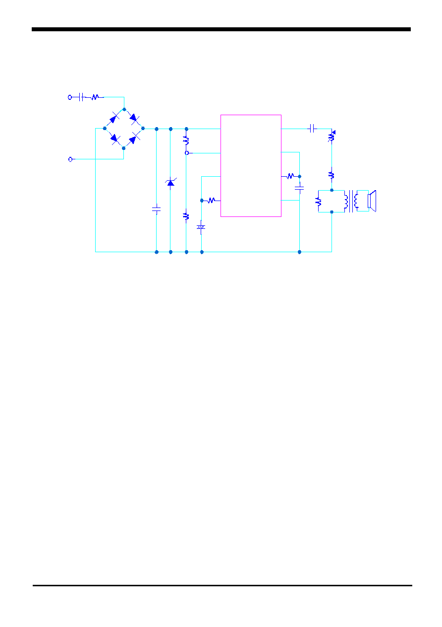
Application Circuit And Information
1.Typical Tone Ringer
The AC ringing voltage appears across the TIP and RING inputs of the circuit and is
attenuated by capacitor(C
1
) and resistor (R
1
). C
1
also provides isolation from DC
voltages(48V) on the line. After full wave rectification by the bridge, the waveform is
filtered by capacitor(C
4
) to provide a DC supply for Tone Ringer chip. As this voltage
exceeds the initiation voltage V
CC(INI)
oscillation starts. With the components shown, the
output frequency chops between f
H1
and f
H2
at a f
L
rate. The loudspeaker load is coupled
through a 1300 to 8 transformer. To prevent DC power supply regulation problems due
to high source impedance of the telephone line and coupling components C
1
and R
1
, while
the output impedance of the 5001P circuit is quite low, the load impedance must be kept
fairly high. The output coupling capacitor (C
5
) is required with transformer coupled loads.
The variable resistor (R
6
) is used to adjust the audio amplitude and resistor (R
4
) is a
current limiting resistor. Resistor R
5
is a quenching resistor used to limit back emf
generated by the inductive load when ringing stops. When driving a piezo-ceramic
transducer type load, the coupling capacitor (C
5
) is not required. However, a current
limiting resistor is required as is a 29V zener diode in parallel with the transducer. This
diode limits the voltage transients than can be generated by mechanical shocking of piezo-
ceramic transducer.
In the 5002P circuit, the initiation supply current I
CC(INI)
can be changed by using external
resistor(R
SL
). The resistor (R
SL
) is connected to GND from pin2. As this initiation voltage
remains constant independent of R
SL
, the supply initiation current f
CC(INI)
varies inversely
with R
SL
. Thus, increasing the value of R
SL
will decrease the amount of AC ringing current
required to trigger the device. R
SL
can also be used to compensated for smaller AC line
SL5001P/2P
DBL5001
1
8
2
7
3
6
4
5
165K
C5
R4
510
R3
C3
R5
R2
S P
191K 0.0068u F
10K
R6
R
E
R
SL
D1
C4
C2
15K
0.22u F
0.047u F
10u F
29V
TIP
1u F
2K
RING
5001
5002
1300 : 8
SL5001P
SL5002P

KSI-W012-001
5
Application Circuit And Information (continued)
coupling capacitors which can be used to alter the ringer equivalence number of a tone
ringer circuit I
CC
-V
CC
(5002P) graph in typical performance characteristic illustrates the
variation of supply current with supply voltage. Curve B(RSL=6.8k) shows the I
CC
-V
CC
characteristic for 5001P circuit Tone Ringer. Curve A is a plot with R
SL
< 6.8 K and shows
a increase in the current drawn up to the initiation voltage V
CC(INI).
The I
CC
-V
CC
characteristic
after initiation remains unchanged. Curve C shows the effect of increasing RSL above 6.8 K
. Initiation current decreases but again current after triggering is unchanged.
2. Pin 2 Input Equivalent Circuit(5001P)
Usually pin 2 is used at an open state, but in the 5001P circuit the trigger in terminal may
be used to externally trigger oscillation for voltage in the range V
SUS
V
CC
V
CC(INI)
or
disable ringer operation. The ringer circuit can only oscillate when Q
1
and Q
2
are conducting.
Normally when supply voltage V
CC
exceeds the supply initiation voltage V
CC(INI)
base Current
flows into Q
1
via D
1
causing Q
1
and Q
2
conduct. This continues until V
CC
is taken below the
minimum sustaining voltage (V
SUS
).
SL5001P/2P
D
1
D
2
P I N2
R
1
Q
1
Q
2
300K