1
Features
·
TS68000/TS68008 Microprocessor Core Supporting a 16- or 8-bit TS68000 Family
·
System Integration Block Including:
Independent Direct Memory Access (IDMA) Controller
Interrupt Controller with Two Modes of Operation
Parallel Input/output (I/O) Ports, some with Interrupt Capability
On-chip Usable 1152 bytes of Dual-port Random-access Memory (RAM)
Three Timers, including a Watchdog Timer
Four Programmable Chip-select Lines with Wait-state Logic
Programmable Address Mapping of Dual-port RAM and IMP Registers
On-chip Clock Generator with an Output Clock Signal
System Control:
System Control Register
Bus Arbitration Logic with Low Interrupt Latency Support
Hardware Watchdog for Monitoring Bus Activity
Low Power (Standby) Modes
Disable CPU Logic (TS68000)
Freeze Control for Debugging Selected On-chip Peripherals
DRAM Refresh Controller
·
Communications Processor Including:
Main Controller (RISC Processor)
Three Full-duplex Serial Communication Controllers (SCCs)
Six Serial Direct Memory Access (SDMA) Channels Dedicated to the Three SCCs
Flexible Physical Interface Accessible by SCCs for Interchip Digital Link (IDL)
General Circuit Interface (GCI, see note), Pulse Code Modulation (PCM), and
Nonmultiplexed Serial Interface (NMSI) Operation
Serial Communication Port (SCP) for Synchronous Communication, Clock Rate up
to 4.096 MHz
Serial Management Controllers (SMCs) for IDL and GCI Channels
·
Frequency of Operation: 16.67 MHz
·
Power Supply: 5 V
DC
± 10%
Description
The IMP is a very large-scale integration (VLSI) device incorporating the main building
blocks needed for the design of a wide variety of controllers. The device is especially
suitable to applications in the communications industry. The IMP is the first device to
offer the benefits of a closely coupled, industry-standard, TS68000/TS68008 micro-
processor core and a flexible communications architecture. This multichannel
communications device may be configured to support a number of popular industry
interfaces, including those for the integrated services digital network (ISDN) basic rate
and terminal adapter applications. Through a combination of architectural and pro-
grammable features, concurrent operation of different protocols is easily achieved
using the IMP. Data concentrators, line cards, bridges, and gateways are examples of
suitable applications for this versatile device.
The IMP is a high-density complementary metal-oxide semiconductor (HCMOS)
device consisting of a TS68000/TS68008 microprocessor core, a system integration
block (SIB), and a communications processor (CP). The TS68302 block diagram is
shown in Figure 1.
Note:
GCI is sometimes referred to as IOM2.
Integrated
Multiprotocol
Processor (IMP)
TS68302
Rev. 2117AHIREL11/02

2
TS68302
2117AHIREL11/02
Screening/Quality
This product is manufactured in full compliance with either:
·
MIL-STD-883 (class B)
·
DESC. Drawing 5962-93159
·
Or according to Atmel standards
Introduction
The TS68302 integrated multiprotocol processor (IMP) is a very large-scale integration
(VLSI) device incorporating the main building blocks needed for the design of a wide
variety of controllers. The device is especially suitable to applications in the communica-
tions industry. The IMP is the first device to offer the benefits of a closely coupled,
industry-standard TS68000 microprocessor core and a flexible communications archi-
tecture. The IMP may be configured to support a number of popular industry interfaces,
including those for the Integrated Services Digital Network (ISDN) basic rate and termi-
nal adapter applications. Concurrent operation of different protocols is easily achieved
through a combination of architectural and programmable features. Data concentrators,
line cards, bridges, and gateways are examples of suitable applications for this device.
The IMP is a high-density complementary metal-oxide semiconductor (HCMOS) device
consisting of a TS68000 microprocessor core, a system integration block (SIB), and a
communications processor (CP).
Figure 1 is a block diagram of the TS68302. The processor can be divided into two main
sections: the bus controller and the micromachine. This division reflects the autonomy
with which the sections operate.
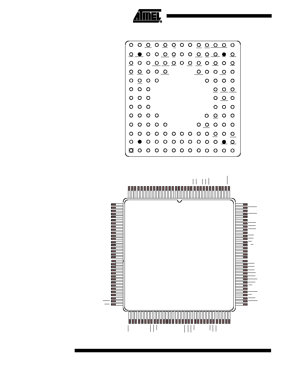
R suffix
PGA 132
(Ceramic Pin Grid Array)
A suffix
CERQUAD 132
(Ceramic Quad Flat Pack)

3
TS68302
2117AHIREL11/02
Figure 1. TS68302 Block Diagram
TS68000/TS68008 CORE
TS68000 BUS
INTERRUPT
CONTROLLER
BUS ARBITER
TIMERS (3)
PARALLEL I/O
1152 BYTES
DUAL-PORT
STATIC RAM
CHIP-SELECT
AND WAIT-
STATE LOGIC
SYSTEM
CONTROL
CLOCK
GENERATOR
ON-CHIP PERIPHERALS BUS INTERFACE UNIT
SERIAL CHANNELS PHYSICAL INTERFACE
I/O PORTS AND PIN ASSIGNEMENTS
COMMUNICATIONS PROCESSOR
MAIN
CONTROLLER
(RISC)
SDMA
(6 CHANNELS)
SMC (2)
SCC1
SCC2
SCC3
SCP
PERIPHERAL BUS
SYSTEM INTEGRATION BLOCK
IDMA
(1 CHANNEL)
DRAM
REFRESH
CONTROLLER
TS68000/TS68008 CORE