
1
Features
À
Comprehensive Library of Standard Logic Cells
À
ATC25 I/O Cells Designed to Operate with V
DD
= 2.5V ▒ 0.25V as Main Target Operating
Conditions
À
IO33 Pad Library Provides Interface to 3V Environment
À
Oscillators Provide Stable Clock Sources
À
Basic Analog Input/Output, Power, Ground and Multiplexer Cells Available,
High-performance Analog Cells Can Be Developed on Request
À
Memory Cells Compiled to the Precise Requirements of the Design
À
Compatible with Atmel's Extensive Range of Microcontroller, DSP, Standard Interface
and Application Specific Cells
Description
The Atmel ATC25 CBIC family is fabricated on a proprietary 0.25 micron five-layer-
metal CMOS process intended for use with a supply voltage of 2.5V ▒ 0.25V. The fol-
lowing table shows the range for which Atmel library cells have been characterized.
The Atmel cell libraries and megacell compilers have been designed in order to be
compatible with each other. Simulation representations exist for three types of operat-
ing conditions; they correspond to three characterization conditions defined as follows:
À
MIN conditions:
T
J
= -40
░C
V
DD
(cell) = 2.75V
Process = fast (industrial best case)
À
TYP conditions:
T
J
= +25
░C
V
DD
(cell) = 2.5V
Process = typ (industrial typical case)
À
MAX conditions:
T
J
= +100
░C
V
DD
(cell) = 2.25V
Process = slow (industrial worst case)
Delays to tri-state are defined as delay to turn off (VGS < VT) of the driving devices.
Output pad drain current corresponds to the output current of the pad when the output
voltage is V
OL
or V
OH
. The output resistor of the pad and the voltage drop due to
access resistors (in and out of the die) are taken into account. In order to have accu-
rate timing estimates, all characterization has been run on electrical netlists extracted
from the layout database.
Table 1. Recommended Operating Conditions
Symbol
Parameter
Conditions
Min
Typ
Max
Unit
V
DD
DC Supply Voltage
Core and Standard I/Os
2.25
2.5
2.75
V
V
DD3
DC Supply Voltage
3V Interface I/Os
3
3.3
3.6
V
V
I
DC Input Voltage
0
V
DD
V
V
O
DC Output Voltage
0
V
DD
V
TEMP
Operating Free Air
Temperature Range
Industrial
-40
+85
░C
Cell-based ASIC
ATC25
Summary
Rev. 1306DS¡CBIC¡09/02
2
ATC25 Summary
1306DS¡CBIC¡09/02
Standard Cell Library
SClib
The Atmel Standard Cell Library, SClib, contains a comprehensive set of combinational
logic and storage cells. The SClib library includes cells which belong to the following
categories:
À
Buffers and Gates
À
Multiplexers
À
Flip-flops
À
Scan Flip-flops
À
Latches
À
Adders and Subtractors
Decoding the Cell Name
The table below shows the naming conventions for the cells in the SClib library. Each
cell name begins with either a two-, three-, or four-letter code that defines the type of
cell. This indicates the range of standard cells available.
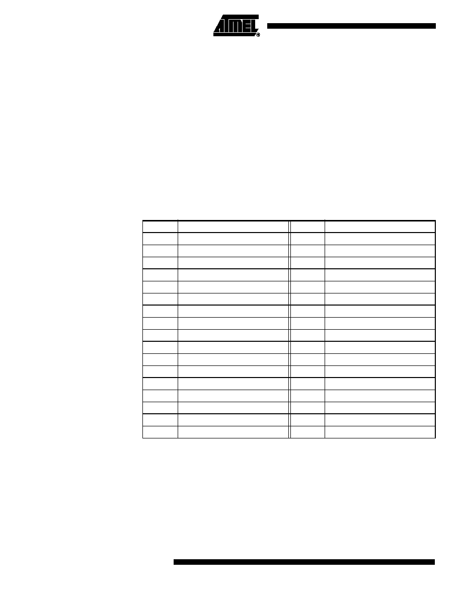
Table 2. Cell Codes
Code
Description
Code
Description
AD
Adder
INVT
Inverting 3-State Buffer
AH
Half Adder
JK
JK Flip-Flop
AS
Adder/Subtractor
LA
D Latch
AN
AND Gate
MI
Inverting Multiplexer
AOI
AND-OR-Invert Gate
MX
Multiplexer
AON
AND-OR-AND-Invert Gates
ND
NAND Gate
AOR
AND-OR Gate
NR
NOR Gate
BH
Bus Holder
OAI
OR-AND-Invert Gate
BUFB
Balanced Buffer
OAN
OR-AND-OR-Invert Gates
BUFF
Non-Inverting Buffer
OR
OR Gate
BUFT
Non-Inverting 3-State Buffer
ORA
OR-AND Gate
CG
Carry Generator
SD
Multiplexed Scan D Flip-Flop
CLK2
Clock Buffer
SE
Multiplexed Scan Enable D Flip-Flop
DE
D-Enabled Flip-Flop
SRLA
Set/Reset Latches with NAND input
DF
D Flip-Flop
SU
Subtractor
INV0
Inverter
XN
Exclusive NOR Gate
INVB
Balanced Inverter
XR
Exclusive OR Gate

4
ATC25 Summary
1306DS¡CBIC¡09/02
Input/Output Pad Cell
Libraries
IO25lib and IO33lib
The Atmel Input/Output Cell Library, IO25lib, contains a comprehensive list of input, out-
put, bidirectional and tristate cells. The ATC25 (2.5V) cell library includes a special set
of I/O cells, IO33lib, for interfacing with external 3V devices.
Voltage Levels
The IO25lib library is made up exclusively of low-voltage chip interface circuits powered
by a voltage in the range of 2.25V to 2.75V. The library is compatible with the SClib 2.5-
volt standard cells library.
Power and Ground Pads
Designers are strongly encouraged to provide three kinds of power pairs for the IO25lib
library. These are "AC", "DC" and core power pairs. AC power is used by the I/O to
switch its output from one state to the other. This switching generates noise in the AC
power buses on the chip. DC power is used by the I/O to maintain its output in a steady
state. The best noise performance is achieved when the DC power buses on the chip
are free of noise; designers are encouraged to use separate power pairs for AC and DC
power to prevent most of the noise in the AC power buses from reaching the DC power
buses. The same power pairs can be used to supply both DC power to the I/Os and
power to the core without affecting noise performance.
Table 6. VSS Power Pad Combinations
Core
Switching I/O
Quiet I/O
Library Cell
Name
Signal Name
Vssi
VssAC
VssDC
À
pv25i00
VSS
À
pv25a00
VSS
À
pv25d00
VSS
À
À
pv25e00
VSS
À
À
pv25b00
VSS
À
À
À
pv25f00
VSS
Table 7. VDD Power Pad Combinations
Core
Switching I/O
Quiet I/O
Library Cell
Name
Signal Name
Vddi
VddAC
VddDC
À
pv25i25
VDD
À
pv25a25
VDD
À
pv25d25
VDD
À
À
pv25e25
VDD
À
À
pv25b25
VDD
À
À
À
pv25f25
VDD

