Rev. 4696C�4BMCU�02/04
Features
�
2-Kbyte ROM, 256
�
4-bit RAM
�
12 Bi-directional I/Os
�
Up to 6 External/Internal Interrupt Sources
�
Multifunction Timer/Counter with
� IR Remote Control Carrier Generator
� Bi-phase-, Manchester- and Pulse-width Modulator and Demodulator
�
Programmable System Clock with Prescaler and Five Different Clock Sources
�
Wide Supply-voltage Range (1.8 V to 6.5 V)
�
Very Low Sleep Current (< 1 �A)
�
32
�
16-bit EEPROM (ATAR890 only)
�
Synchronous Serial Interface (2-wire, 3-wire)
�
Watchdog, POR and Brown-out Function
�
Voltage Monitoring Inclusive Lo_BAT Detection
�
Flash Controller ATAM893 Available (SSO20)
Description
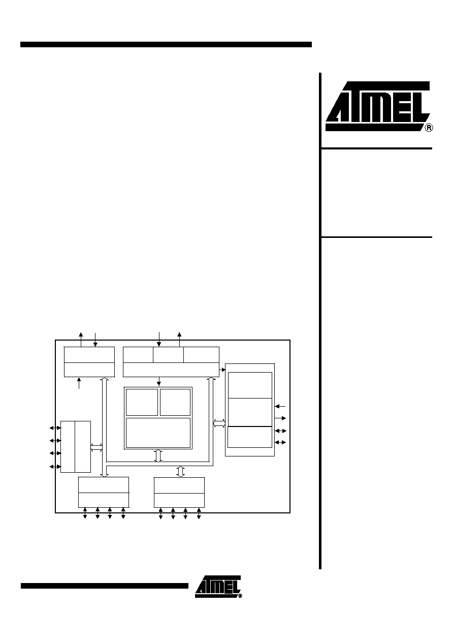
The ATAR090 and ATAR890 are members of Atmel's family of 4-bit single-chip micro-
controllers. They offer the highest integration for IR and RF data communication and
remote-control. The ATAR090 and ATAR890 are suitable for the transmitter side. They
contain ROM, RAM, parallel I/O por ts, two 8-bit programmable multifunction
timer/counters with modulator and demodulator function, voltage supervisor, interval
timer with watchdog function and a sophisticated on-chip clock generation with exter-
nal clock input, integrated RC-, 32-kHz crystal- and 4-MHz crystal-oscillators. The
ATAR890 has an additional EEPROM as a second chip in one package.
Figure 1. Block Diagram
Voltage monitor
External input
MARC4
UTCM
OSC1
I/O bus
ROM
RAM
4-bit CPU core
256 x 4 bit
V
DD
V
SS
Data direction +
alternate function
Data direction +
interrupt control
Port 4
Port 5
Brown-out protect
RESET
Clock management
Timer 1
watchdog timer
Timer 2
Serial interface
Por
t
2
Data di
r
e
c
t
i
o
n
T2O
SD
SC
BP20/NTE
BP21
BP22
BP23
BP40
INT3
SC BP41
VMI
T2I
BP42
T2O
BP43
INT3
SD
BP50
INT6
BP51
INT6
BP52
INT1
BP53
INT1
RC
oscillators
Crystal
oscillators
2 K x 8 bit
VMI
with modulator
SSI
External
clock input
interval- and
8/12-bit timer
T2I
OSC2
Low-current
Microcontroller
for Wireless
Communication
ATAR090
ATAR890
2
ATAR090/ATAR890
4696C�4BMCU�02/04
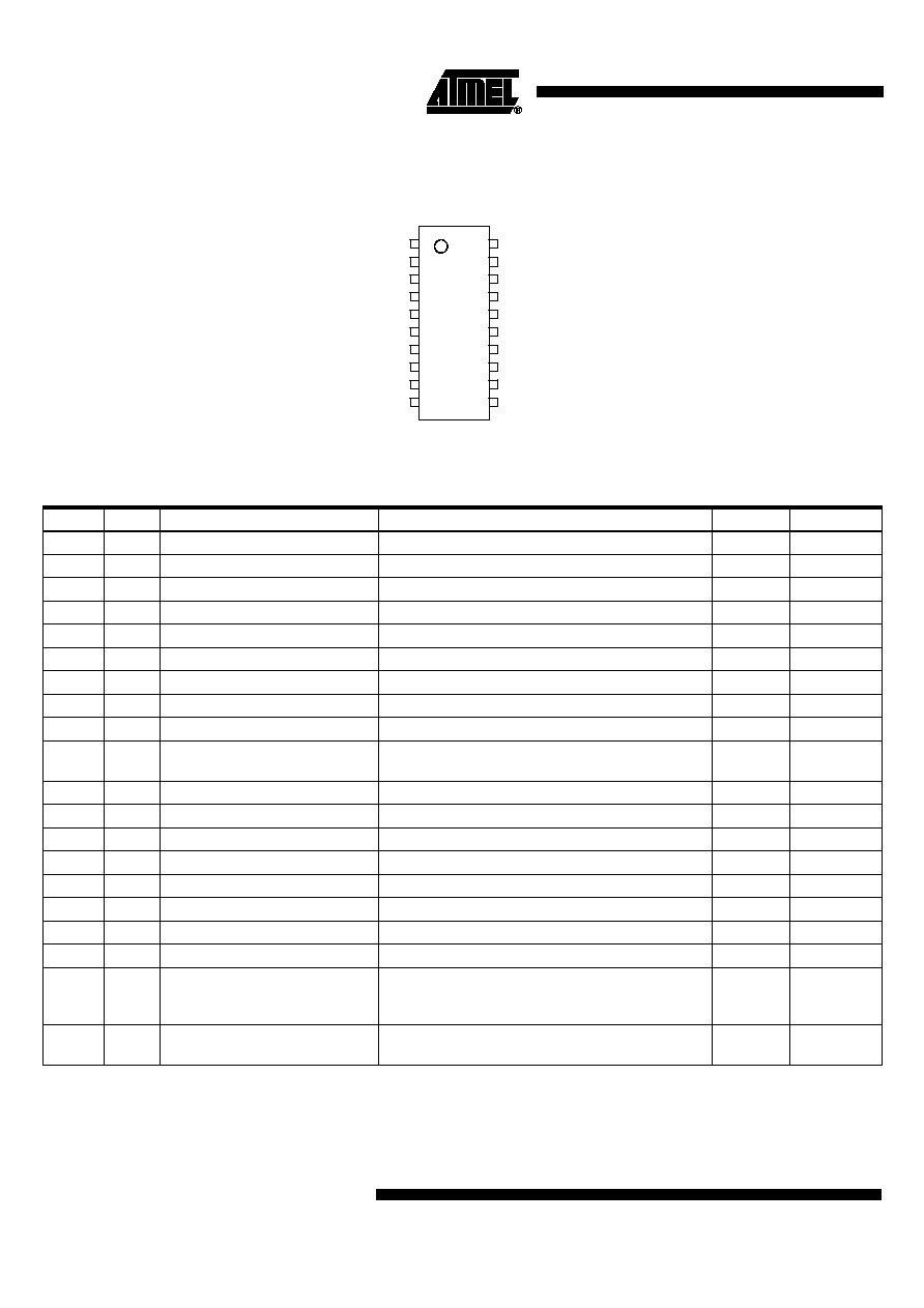
Pin Configuration
Figure 2. Pinning SSO20
Pin Description
Name
Type
Function
Alternate Function
Pin No.
Reset State
VDD �
Supply
voltage
�
1
NA
VSS
�
Circuit ground
�
20
NA
NC
�
Not connected
�
10
�
NC
�
Not connected
�
11
�
BP20
I/O
Bi-directional I/O line of Port 2.0
NTE � test mode enable, see section "Master Reset"
13
Input
BP21
I/O
Bi-directional I/O line of Port 2.1
�
14
Input
BP22
I/O
Bi-directional I/O line of Port 2.2
�
15
Input
BP23
I/O
Bi-directional I/O line of Port 2.3
�
16
Input
BP40
I/O
Bi-directional I/O line of Port 4.0
SC serial clock or INT3 external interrupt input
2
Input
BP41
I/O
Bi-directional I/O line of Port 4.1
VMI voltage monitor input or T2I external clock input
Timer 2
17
Input
BP42
I/O
Bi-directional I/O line of Port 4.2
T2O Timer 2 output
18
Input
BP43
I/O
Bi-directional I/O line of Port 4.3
SD serial data I/O or INT3-external interrupt input
19
Input
BP50
I/O
Bi-directional I/O line of Port 5.0
INT6 external interrupt input
6
Input
BP51
I/O
Bi-directional I/O line of Port 5.1
INT6 external interrupt input
5
Input
BP52
I/O
Bi-directional I/O line of Port 5.2
INT1 external interrupt input
4
Input
BP53
I/O
Bi-directional I/O line of Port 5.3
INT1 external interrupt input
3
Input
NC
�
Not connected
�
9
�
NC
�
Not connected
�
12
�
OSC1
I
Oscillator input
4-MHz crystal input or 32-kHz crystal input or
external clock input or external trimming resistor
input
7
Input
OSC2
O
Oscillator output
4-MHz crystal output or 32-kHz crystal output or
external clock input
8
NA
VDD
BP40/INT3/SC
BP53/INT1
BP52/INT1
BP51/INT6
BP50/INT6
OSC1
OSC2
NC
NC
VSS
BP43/INT3/SD
BP42/T2O
BP41/VMI/T2I
BP23
BP22
BP21
BP20/NTE
NC
NC
1
2
3
4
5
6
7
8
9
10
20
19
18
17
16
15
14
13
12
11
3
ATAR090/ATAR890
4696C�4BMCU�02/04
Introduction
The ATAR090/ATAR890 are members of Atmel's family of 4-bit single-chip microcon-
trollers. They contain ROM, RAM, parallel I/O ports, one 8-bit programmable multi-
function timer/counters, voltage supervisor, interval timer with watchdog function and a
sophisticated on-chip clock generation with integrated RC-, 32-kHz crystal- and 4-MHz
crystal oscillators. Table 2 provides an overview of the available variants.
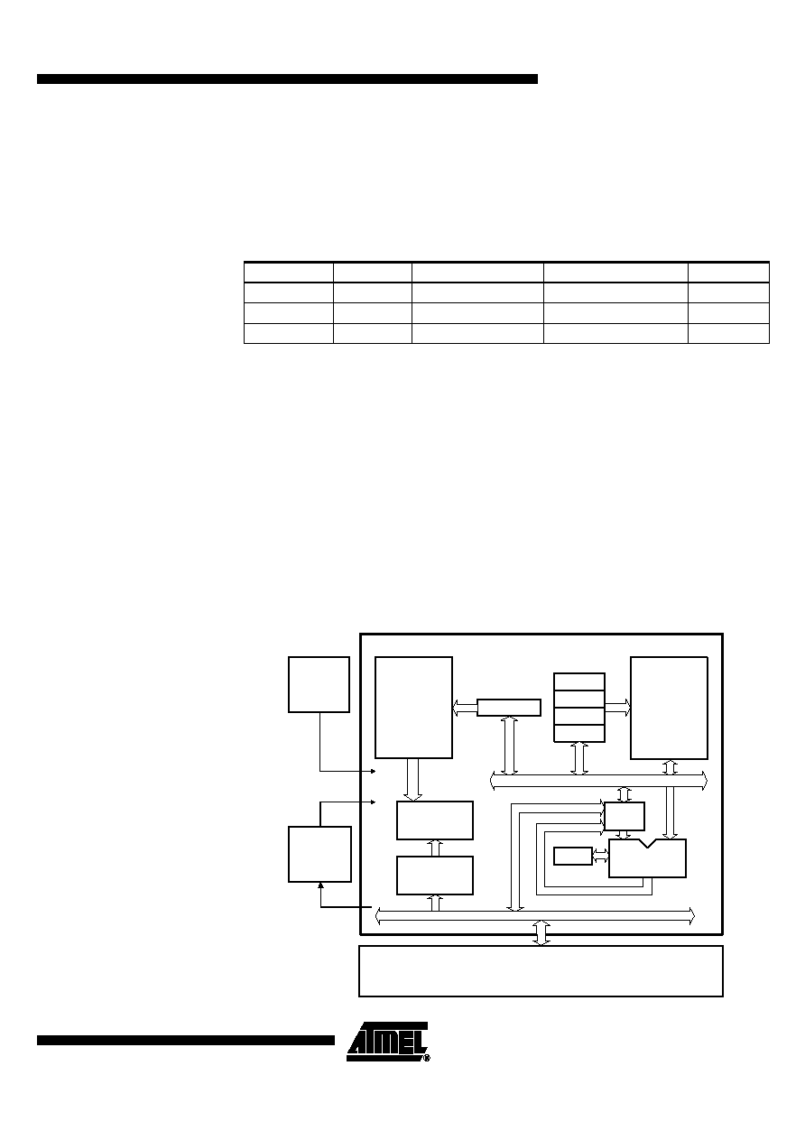
MARC4 Architecture
General Description
The MARC4 microcontroller consists of an advanced stack-based, 4-bit CPU core and
on-chip peripherals. The CPU is based on the HARVARD architecture with physically
separate program memory (ROM) and data memory (RAM). Three independent buses,
the instruction bus, the memory bus and the I/O bus, are used for parallel communica-
tion between ROM, RAM and peripherals. This enhances program execution speed by
allowing both instruction prefetching, and a simultaneous communication to the on-chip
peripheral circuitry. The extremely powerful integrated interrupt controller with associ-
ated eight prioritized interrupt levels supports fast and efficient processing of hardware
events. The MARC4 is designed for the high-level programming language qFORTH.
The core includes both an expression and a return stack. This architecture enables
high-level language programming without any loss of efficiency or code density.
Figure 3. MARC4 Core
Table 1. Available Variants of ATAxx9x
Version
Type
ROM
E2PROM Peripheral
Packages
Flash device
ATAM893
4-Kbyte EEPROM
64 byte
SSO20
Production
ATAR090 2-Kbyte
mask
ROM
�
SSO20
Production
ATAR890
2-Kbyte mask ROM
64 byte
SSO20
Instruction
decoder
CCR
TOS
ALU
RAM
RP
X
Y
Program
256 x 4-bit
MARC4 CORE
Clock
Reset
Sleep
Memory bus
I/O bus
Instruction
bus
Reset
System
clock
Interrupt
controller
On-chip peripheral modules
memory
SP
PC
4
ATAR090/ATAR890
4696C�4BMCU�02/04
Components of MARC4
Core
The core contains ROM, RAM, ALU, program counter, RAM address registers, instruc-
tion decoder and interrupt controller. The following sections describe each functional
block in more detail.
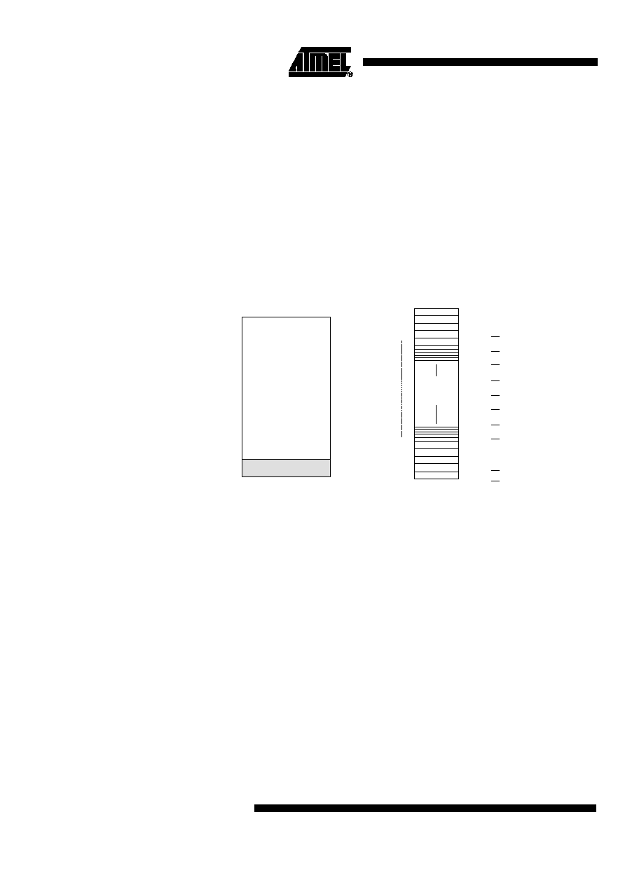
ROM
The program memory (ROM) is mask programmed with the customer application pro-
gram during fabrication of the microcontroller. The ROM is addressed by a 12-bit wide
program counter, thus predefining a maximum program bank size of 2 Kbytes. An addi-
tional 1 Kbyte of ROM exists which is reserved for quality control self-test software The
lowest user ROM address segment is taken up by a 512-byte zero page which contains
predefined start addresses for interrupt service routines and special subroutines acces-
sible with single byte instructions (SCALL).
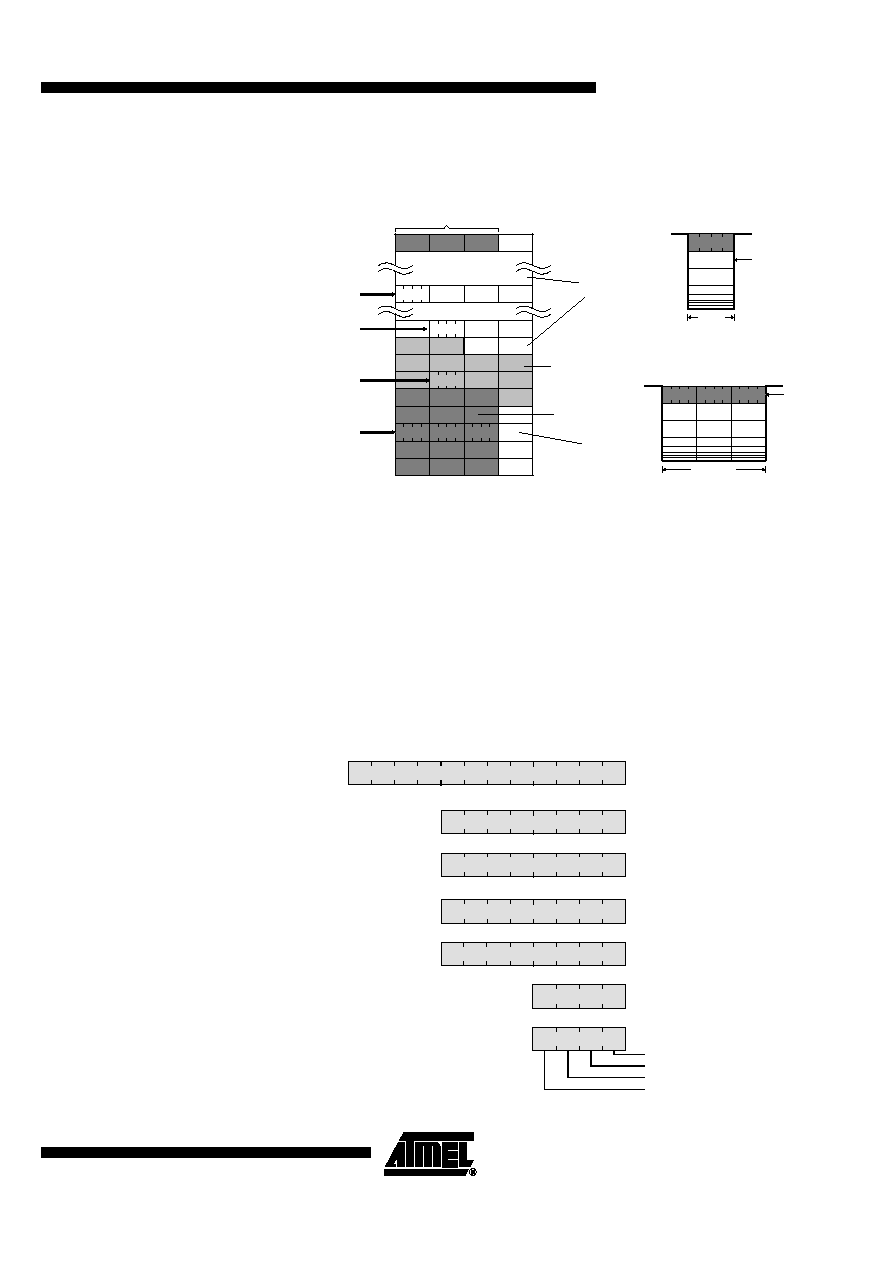
The corresponding memory map is shown in Figure 4 Look-up tables of constants can
also be held in ROM and are accessed via the MARC4's built-in table instruction.
Figure 4. ROM Map
RAM
The ATAR090 and ATAR890 contain 256 x 4-bit wide static random access memory
(RAM). It is used for the expression stack, the return stack and data memory for vari-
ables and arrays. The RAM is addressed by any of the four 8-bit wide RAM address
registers SP, RP, X and Y.
Expression Stack
The 4-bit wide expression stack is addressed with the expression stack pointer (SP). All
arithmetic, I/O and memory reference operations take their operands from, and return
their results to the expression stack. The MARC4 performs the operations with the top of
stack items (TOS and TOS-1). The TOS register contains the top element of the expres-
sion stack and works in the same way as an accumulator. This stack is also used for
passing parameters between subroutines and as a scratch pad area for temporary stor-
age of data.
Return Stack
The 12-bit wide return stack is addressed by the return stack pointer (RP). It is used for
storing return addresses of subroutines, interrupt routines and for keeping loop index
counts. The return stack can also be used as a temporary storage area.
The MARC4 instruction set supports the exchange of data between the top elements of
the expression stack and the return stack. The two stacks within the RAM have a user
definable location and maximum depth.
ROM
(2 K x 8 bit)
Zero page
7FFh
1FFh
000h
1F0h
1F8h
010h
018h
000 h
008h
020 h
1E8h
1E0h
SC
ALL addresses
140h
180h
040h
0C 0h
008h
$A U T O SL E E P
$R E SE T
I N T 0
I N T 1
I N T 2
I N T 3
I N T 4
I N T 5
I N T 6
I N T 7
1 E0h
1C 0h
100h
080h
Z er o
p age
000h
5
ATAR090/ATAR890
4696C�4BMCU�02/04
Figure 5. RAM Map
Registers
The MARC4 controller has seven programmable registers and one condition code regis-
ter. They are shown in the following programming model (see Figure 6).
Program Counter (PC)
The program counter is a 12-bit register which contains the address of the next instruc-
tion to be fetched from ROM. Instructions currently being executed are decoded in the
instruction decoder to determine the internal micro-operations. For linear code (no calls
or branches) the program counter is incremented with every instruction cycle. If a
branch-, call-, return-instruction or an interrupt is executed, the program counter is
loaded with a new address. The program counter is also used with the table instruction
to fetch 8-bit wide ROM constants.
Figure 6. Programming Model
RAM
FCh
00h
Autosleep
FFh
03h
04h
X
Y
SP
RP
TOS-1
Expression
stack
Return
stack
Global
variables
R
A
M address re
gister:
07h
(256 x 4-bit)
Global
variables
4-bit
TOS
TOS-1
TOS-2
3
0
SP
Expression stack
Return stack
0
11
12-bit
RP
v
TOS
CCR
0
3
0
3
0
7
0
7
0
7
0
11
RP
SP
X
Y
PC
--
B
I
Program counter
Return stack pointer
Expression stack pointer
RAM address register (X)
RAM address register (Y)
Top of stack register
Condition code register
Carry/borrow
Branch
Interrupt enable
Reserved
0
7
C
0
0