
Note: This is a summary document. A complete document is available
under NDA. For more information, please contact your local Atmel
sales office.
Features
Ě
One of a Family of Devices with User Memory of 1 Kbit to 64 Kbits
Ě
Contactless 13.56 MHz RF Communications Interface
ş ISO/IEC 14443-2:2001 Type B Compliant
ş ISO/IEC 14443-3:2001 Type B Compliant Anticollision Protocol
ş Command Set Optimized for Multicard RF Communications
ş Tolerant of Type A Signaling for Multiprotocol Applications
ş Operating Distance Up to 10 cm
Ě
Integrated 82 pF Tuning Capacitor
Ě
User EEPROM Memory
ş 1 Kbits Configured as Four 32-byte (256-bit) User Zones
ş Byte, Page, and Partial Page Write Modes
ş Self-timed Write Cycle
Ě
256-byte (2-Kbit) Configuration Zone
ş User-programmable Application Family Identifier (AFI)
ş User-defined Anticollision Polling Response
ş User-defined Keys and Passwords
Ě
High-Security Features
ş 64-bit Mutual Authentication Protocol (under exclusive patent license from ELVA)
ş Encrypted Checksum
ş Stream Encryption
ş Four Key Sets for Authentication and Encryption
ş Eight Sets of Two 24-bit Passwords
ş Password and Authentication Attempts Counters
ş Selectable Access Rights by Zone
ş Write Lock Mode
ş Antitearing Function
ş Tamper Sensors
Ě
High Reliability
ş Endurance: 100,000 Write Cycles
ş Data Retention: 10 Years
ş Operating Temperature:
-40░C to +85░C
CryptoRF
TM
EEPROM Memory
1 Kbits
AT88SC0104CRF
Summary
Rev. 5021ASşCRRFş05/03

2
AT88SC0104CRF
5021ASşCRRFş05/03
Description
The CryptoRF
TM
family integrates a 13.56 Mhz RF interface into a CryptoMemory
«
,
resulting in a contactless smart card with advanced security and cryptographic features.
This device is optimized as a contactless secure memory, for multiapplication RF smart
card markets, and secure identification for electronic data transfer, without the
requirement of an internal microprocessor.
For communications, the RF interface utilizes the ISO 14443-2 and -3 Type B bit timing
and signal modulation schemes, and the ISO 14443-3 Slot-MARKER Anticollision
Protocol. Data is exchanged half duplex at a 106-kbit/s rate, with a two-byte CRC_B
providing error detection capability. The maximum communication range between the
reader antenna and contactless card is approximately 10 cm when used with an RFID
reader that transmits the maximum ISO 14443-2 RF power level. The RF interface
powers the other circuits; no battery is required. Full compliance with the ISO 14443-2
and -3 standards results in anticollision interoperability with the AT88RF020 2-Kbit RFID
EEPROM product and provides both a proven RF communication interface and a robust
anticollision protocol.
The AT88SC0104CRF contains 1 Kbits of user memory and 2 Kbits of system memory.
The 2 Kbits of system zone memory contain eight sets of read/write passwords, four
crypto key sets, security access registers for each user zone, and password/key
registers for each zone. The features and functionality of the system zone are identical
to those in the standard CryptoMemory.
The CryptoRF command set is optimized for a multicard RF communications
environment and includes all of the functionality of the standard CryptoMemory
commands. A programmable AFI register allows this IC to be used in numerous
applications in the same geographic area with seamless discrimination of cards
assigned to a particular application during the anticollision process.

3
AT88SC0104CRF
5021ASşCRRFş05/03
Block Diagram
Figure 1. Block Diagram
Communications
All personalization and communication with this device is performed through the RF
interface. The IC includes an integrated tuning capacitor, enabling it to operate with only
the addition of a single external coil antenna.
The RF communications interface is fully compliant with the electrical signaling and RF
power specifications in ISO/IEC 14443-2:2001 for Type B only. Anticollision operation and
frame formatting are compliant with ISO/IEC 14443-3:2001 for Type B only.
ISO/IEC 14443 nomenclature is used in this specification where applicable. The
following abbreviations are utilized throughout this document. Additional terms are
defined in the section in which they are used.
Ě
PCD ş Proximity Coupling Device: the reader/writer and antenna.
Ě
PICC ş Proximity Integrated Circuit Card: the tag/card containing the IC and
antenna.
Ě
ETU ş Elementary Time Unit: the time required to transmit or receive one data bit.
One ETU is equal to 128 carrier cycles (9.439 microseconds).
Ě
RFU ş Reserved for Future Use: any feature, memory location, or bit that is held as
reserved for future use
Ě
$ xx ş Hexadecimal Number: denotes a hex number "xx" (Most Significant Bit on
left)
Ě
xxxx b ş Binary Number: denotes a binary number "xxxx" (Most Significant Bit on
left)
RF Interface
AC1
C
AC2
Over
Voltage
Clamp
Modulator
VSS
V
DD
Rectifier
Regulator
Clock
Extraction
Data
Extraction
Command
and
Response
EEPROM
Data Transfer
Password
Verification
Frame Formatting
and
Error Detection
Interface
Anticollision
Random Number
Generator
Authentication
Encryption and
Certification Unit

4
AT88SC0104CRF
5021ASşCRRFş05/03
Anticollision Protocol
When the PICC enters the 13.56 Mhz RF field of the host reader (PCD), it performs a
power on reset (POR) function and waits silently for a valid Type B polling command.
The CryptoRF PICC processes the antitearing registers as part of the POR process.
The PCD initiates the anticollision process by issuing an REQB or WUPB command.
The WUPB command activates any card (PICC) in the field with a matching AFI code.
The REQB command performs the same function but does not affect a PICC in the halt
state. The REQB and WUPB commands contain an integer N indicating the number of
slots assigned to the anticollision process. The CryptoRF command set is available only
after the anticollision process has been completed.
CRC Error Detection
A two-byte CRC_B is required in each frame transmitted by the PICC or PCD to permit
transmission error detection. The CRC_B is calculated on all of the command and data
bytes in the frame. For encrypted data, the encryption is performed prior to CRC_B
calculation. The SOF, EOF, start bits, stop bits, and EGT are not included in the CRC_B
calculation. The two-byte CRC_B follows the data bytes in the frame.
Figure 2. Location of the Two CRC_B Bytes within a Frame
The CRC polynomial is defined in ISO/IEC 14443 and ISO/IEC 13239 as x
16
+ x
12
+ x
5
+
x
0
. This is a hex polynomial of $1021. The initial value of the register used for the
CRC_B calculation is all ones ($FFFF). When receiving information from the reader, the
PICC computes the CRC on the incoming command, data, and CRC bytes. After the
last bit has been processed, the CRC register should contain $0000.
Type A Tolerance
The RF Interface is designed for use in multiprotocol applications. It will not latch or lock
up if exposed to Type A signals and will not respond to them. The PICC may reset in the
presence of Type A field modulation but is not damaged by exposure to Type A signals.
SOF
K data bytes
CRC1
CRC2
EOF
5
AT88SC0104CRF
5021ASşCRRFş05/03
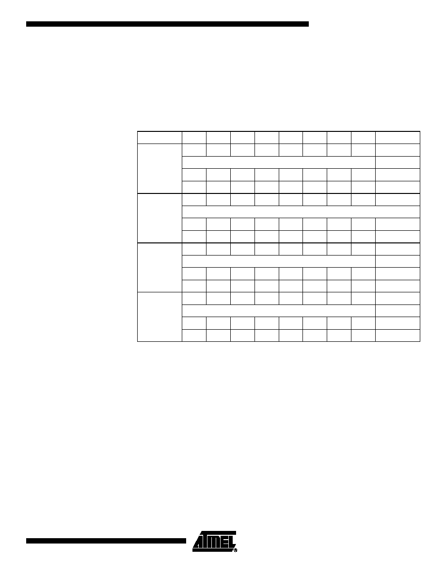
User Memory
The EEPROM user memory is divided into four user zones as shown in the memory
map in Table 1. Multiple zones allow for different types of data or files to be stored in
different zones. Access to the user zones is allowed only after security requirements
have been met. These security requirements are defined by the user in the configuration
zone during personalization of the device. If the same security requirements are
selected for multiple zones, then these zones may be effectively accessed as one larger
zone. The EEPROM memory page length is 16 bytes.
Configuration
Memory
The configuration zone consists of 2048 bits of EEPROM memory used for storing
system data, passwords, keys, codes, and security-level definitions for each user zone.
Access rights to the configuration zone are defined in the control logic and may not be
altered by the user. These access rights include the ability to program certain portions of
the configuration zone and then lock the data written through use of the security fuses.
Security Fuses
There are three fuses on the device that must be blown during the device personaliza-
tion process. Each fuse locks certain portions of the configuration zone as OTP
memory. Fuses are designed for the module manufacturer, card manufacturer and card
issuer and should be blown in sequence, although all programming of the device and
blowing of the fuses may be performed at one final step.
Table 1. Memory Map
Zone
$0
$1
$2
$3
$4
$5
$6
$7
User 0
$00
32 Bytes
ş
ş
$18
User 1
$00
32 Bytes
ş
ş
$18
User 2
$00
32 Bytes
ş
ş
$18
User 3
$00
32 Bytes
ş
ş
$18