
Description
The AT43USB380 is a straightforward upgrade of the AT43USB370 Host/Function
Processor to support the USB 2.0 On-The-Go (OTG) specification. It can operate
either as a single-chip Host/Function Processor or if used in conjunction with an exter-
nal Atmel Charge Pump, as a full OTG solution.
The AT43USB380 is functionally equivalent to the AT43USB370 as a Host/Function
Processor and can be used in place of the AT43USB370 in the existing AT43USB370
design with minor hardware modifications. The pinout differences between the
AT43USB370 and the AT43USB380 are due to the inclusion of the on-chip OTG inter-
face in the AT43USB380.
To support OTG functionality, an external Charge Pump has to be connected to the
OTG interface of the AT43USB380, as shown in Figure 1 on page 7. The external
Charge Pump serves in the following two capacities:
1.
As a power source to the downstream USB devices.
2.
As a signaling interface during the OTG session negotiation upon connection.
From the hardware standpoint, the AT43USB380 is equivalent to the AT43USB370
with the following exceptions:
·
On-chip OTG Interface. This hardware block is added to the AT43USB380 to
support the OTG functionality. Signals in the OTG interface include ID,
DISCHARGE, PUMP, CONTROL, EN, SESS_VLD, SESS_END, SESS_HIGH
and SESS_LOW. This interface is used during an OTG session to determine the
roles of the AT43USB380 and the connected OTG-enabled USB device either as
a host or a function.
·
8/16/32 Bit Generic Host Processor Interface. The AT43USB380 has a variable
width, generic host processor interface whereas the AT43USB370 supports only
32-bit host interface. The width of the host interface on the AT43USB380 is
determined by firmware configuration.
·
Simplified System Interface. The GPIOs required in AT43USB370 for
handshaking are no longer required in AT43USB380. The system processor can
write directly to the AT43USB380 registers thus eliminates the need for PROG,
SEL, READY, DONE, MORE, INTR_IN signals. The WAIT_N signal is not needed
either. It is only there for precaution for SYS_CLK synchronization.
·
Up to 16 GPIO Pins. GPIO pins are multiplexed with the host processor interface.
When the interface to the host processor is 8 or 16 bits, up to 16 of the unused
pins in the host processor interface can be used as GPIO pins. High level APIs
are provided to access these GPIO pins.
From the standpoint of the firmware development environment, the AT43USB380
shares the same high level APIs and low level fir mware librar ies with the
AT43USB370. Additions to the AT43USB380 firmware suite include:
·
High level APIs specific to the OTG support. The number of additional APIs is
less than 10.
·
Low level OTG firmware embedded in the AT43USB380 hardware that support
Host Negotiation Protocol (HNP) and Session Request Protocol (SRP).
The AT43USB380 share the same debugging tools with the AT43USB370 as well.
During development, the AT43USB380 should be treated as a black box in terms of
On-The-Go
Upgrade of the
AT43USB370
USB 2.0
Full-Speed
Host/Function
Processor
AT43USB380
Upgrade Map
Summary
Note: This is a summary document. A complete document
is not available at this time. For more information, please
contact your local Atmel sales office.
3420ASUSB03/04
2
AT43USB380 Upgrade Map Summary
3420ASUSB03/04
USB functionality. Communication with the AT43USB380 is achieved through a small
set (less than 25) of high level, ANSI C-compliant APIs. The actual USB protocol includ-
ing HNP and SRP is transparent to the host processor.
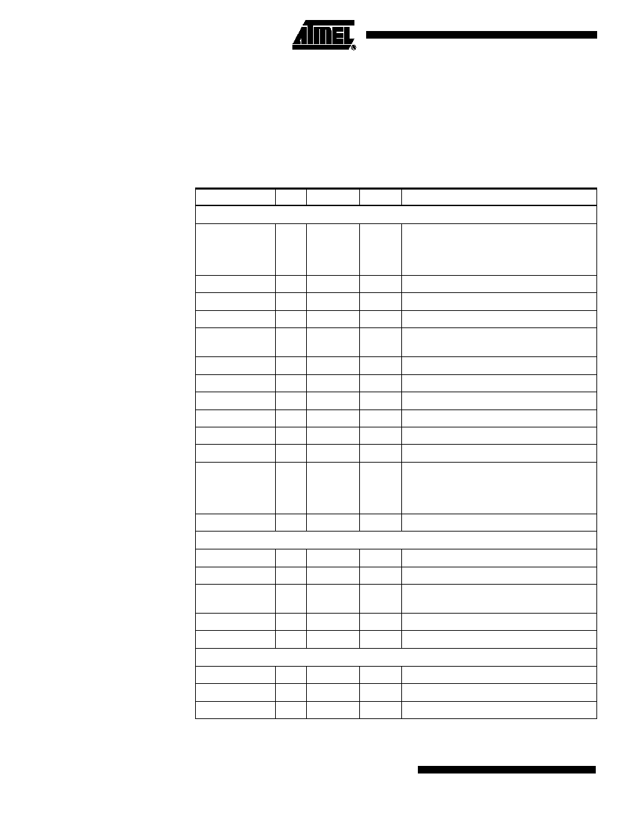
AT43USB380 OTG Processor Pin Description
Table 1 gives the description of the pins.
Table 1. Pin Description of the AT43USB380
Signal Name
Dir.
Polarity
Width
Description
System Interface
SYS_CLK
I
1
Host system clock input for synchronization
of WAIT_N and DREQ_N. (Synchronization
requirement can be enable/disable through
internal register settings)
A[7:0]
I
8
System
Address
Bus
CS_N
I
LO
1
CHIP_SELECT signal from System (ARM
®
)
D[15:0]
B
16
System Data Bus [15:0]
D[31:16]/
GPIO[15:0]
B
16
BWIDTH[1:0]=1x : System Data Bus [31:16]
BWIDTH[1:0]=0x : GPIO[15:0]
DACK_N
I
LO
1
DMA Acknowledge from System (ARM)
DREQ_N
O
LO
1
DMA Request to System (ARM)
INTR_OUT
O
HI
1
Interrupt to System (ARM)
OE_N
I
LO
1
OUTPUT_ENABLE from System (ARM)
WAIT_N
O
LO
1
WAIT to System (ARM)
WE_N
I
LO
1
WRITE_ENABLE from System (ARM)
BWIDTH[1:0]
I
2
System Data Bus Size:
00 : 8 Bit Interface D[7:0]
01 : 16 Bit Interface D[15:0]
1x : 32 Bit Interface D[31:0]
WAKEUP_N
I
LO
1
Wakeup Request from System
USB Interface
DM
B
1
USB
Line
(D-)
DP
B
1
USB
Line
(D+)
ID
I
1
OTG device type identification; used to
differentiate a Mini-A and Mini-B plug
RPU_EN
O
1
Enable resistive pull-up to the D+ line
RPD_EN
O
1
Enable resistive pull-down to the D+/D- lines
Charge Pump Interface
CPClk
O
1
Charge Pump clock output
EN
O
1
Charge Pump; Enable for Charge Pump
PUMP_EN
O
1
Charge Pump; Enable for Charge Pump

3
AT43USB380 Upgrade Map Summary
3420ASUSB03/04
SESS_VLD
I
1
Charge Pump; Active high when VBUS >
VSESS_VLD otherwise "0"
SESS_END
I
1
Charge Pump; Active high when VBUS >
VSESS_END otherwise "0"
SESS_LOW
I
1
Charge Pump; Active high when VBUS >
VSESS_LOW otherwise "0"
SESS_HIGH
I
1
Charge Pump; Active high when VBUS >
VSESS_HIGH otherwise "0"
LOW_CUR
O
1
Limits the current output of the Charge
Pump. Used during VBUS pulsing when
configured as B-device
DISCHARGE
O
1
Charge Pump; Connect VBUS to ground
Oscillator, Clocks
XTAL1
I
1
Oscillator
input
XTAL2
O 1
Oscillator
output
LFT
I
1
PLL loop filter
CLK_SEL
I
1
Clock Source selection between crystal and
external oscillator
RESET_N
I
LO
1
RESET for USB Processor
Jtag Interface
TCK/SI
I
1
TP3=0: JTAG Clock - from JTAG controller;
TP3=1: SI-EEPROM
TDI/SCK
I
1
TP3=0: JTAG Serial Data IN - from JTAG
controller;
TP3=1: SCK-EEPROM
TDO/SO
O
1
TP3=0: JTAG Serial Data OUT - from JTAG
controller;
TP3=1: SO-EEPROM
TMS/CS
I
1
TP3=0: JTAG Mode Select - from JTAG
controller;
TP3=1: CS-EEPROM
TRST_N
I
LO
1
JTAG Reset - from JTAG controller
Test Pins
TP0
I
1
Test pin 0
TP1
I
1
Test Pin 1
TP2
I
1
Test pin 2
TP3
I
1
Test pin 3
TP4/SCAN_EN
I
1
Test pin 4/SCAN_EN
TP_CLK
/D_CLK
O
1
Clock test output/SIE DPLL extracted clock
TP_RCV_DATA
/RCV_DATA
O
1
Extracted serial data test output
Table 1. Pin Description of the AT43USB380 (Continued)
Signal Name
Dir.
Polarity
Width
Description

4
AT43USB380 Upgrade Map Summary
3420ASUSB03/04
AT43USB380 OTG Processor Pin Assignment
Power/Ground Pins
VEXT18
O
3
1.8V regulated output
VDD
I
5
3.3V input
VSS
10
Ground
Table 1. Pin Description of the AT43USB380 (Continued)
Signal Name
Dir.
Polarity
Width
Description
Pin #
Signal
Type
1
A7
Input
2
A6
Input
3
A5
Input
4
A4
Input
5
A3
Input
6
A2
Input
7
A1
Input
8
A0
Input
9
CS_N
Input
10
OE_N
Input
11
WE_N
Input
12
INTR_OUT
Output
13
VSS
Power Supply/Ground
14
VDD18
Power Supply/Ground
15
VDD
Power Supply/Ground
16
SYS_CLK
Input
17
WAIT_N
Output
18
DREQ_N
Output
19
DACK_N
Input
20
CPClk
Output
21
DISCHARGE
Output
22
EN
Output
23
LOW_CUR
Output
24
PUMP_EN
Output
25
SESS_LOW
Input
26
VSS
Power Supply/Ground
27
SESS_VLD
Input
28
SESS_HIGH
Input
29
SESS_END
Input

5
AT43USB380 Upgrade Map Summary
3420ASUSB03/04
30
ID
Input
31
TP0
Input
32
TP1
Input
33
CLK_SEL
Input
34
VSS
Power Supply/Ground
35
XTAL1
Input
36
XTAL2
Output
37
LFT
Input
38
VDD18
Power Supply/Ground
39
VDD
Power Supply/Ground
40
VSS
Power Supply/Ground
41
DM
Bi-directional
42
DP
Bi-directional
43
TP2
Input
44
TP3
Input
45
RPD_EN
Output
46
RPU_EN
Output
47
RESET_N
Input
48
TCK/SI
Input
49
TMS/CS
Input
50
VDD
Power Supply/Ground
51
VSS
Power Supply/Ground
52
TDI/SCK
Input
53
TDO/SO
Output
54
TRST_N
Input
55
TP_CLK/D_CLK
Output
56
TP_RCV_DATA/RCV_DATA
Output
57
TP4/scan_en
Input
58
BWIDTH[0]
Input
59
WAKEUP_N
Input
60
D31/GPIO[15]
Bi-directional
61
D30/GPIO[14]
Bi-directional
62
D29/GPIO[13]
Bi-directional
63
D28/GPIO[12]
Bi-directional
64
VSS
Power Supply/Ground
65
VDD18
Power Supply/Ground
66
VDD
Power Supply/Ground
Pin #
Signal
Type