AT16646
Fast Logic
TM
TM
16-Bit
Tri-State
TM
TM
Register
AT16646F
AT16646G
Features
·
Fastest Propagation Speeds in the Industry T
PD (F grade)
= 2.5 ns, T
PD (G grade)
= 2.0 ns
·
Maximum derating for capacitive loads 1.5ns/100 pF (F grade) and 1.1ns/100 pF
(G grade)
·
Very low ground bounce < 0.6 V @ V
CC
=5.00 V, T
a
=25°C
·
Typical output skew
0.25ns
·
Bus Hold circuitry to retain last active state during Tri-State
TM
TM
·
Available in SSOP and TSSOP packages
Description
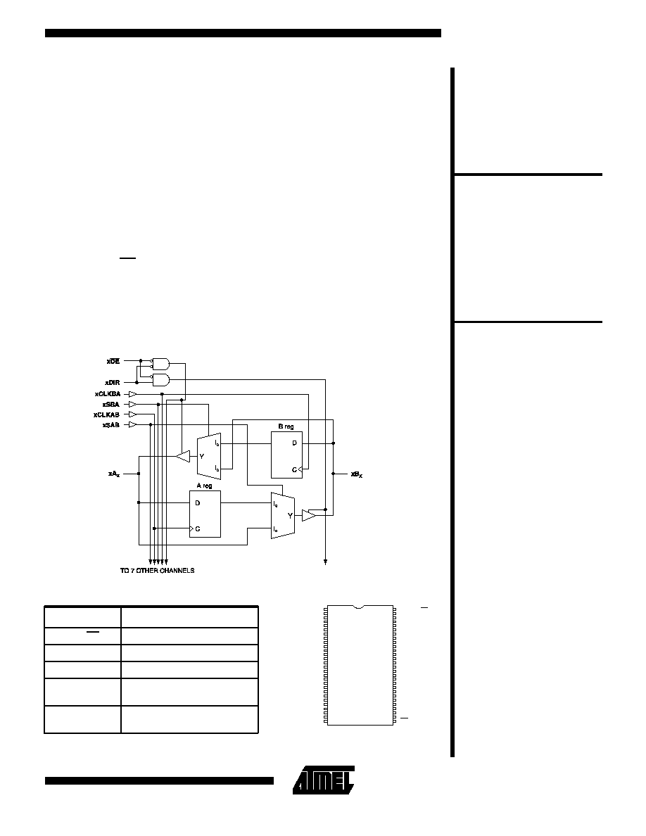
Atmel's AT16646 devices are 16-bit high speed, low power Tri-statable D type
registers, ideal for use in systems requiring both transparent and registered mode
functions. They are organized as two separate 8-bit bus transceivers. Data flow is
bi-directional, and can be controlled for multiplexed transmission between A bus and
B bus either directly or from the D registers by use of the direction control pin (xDir),
output enable (xOE), and select lines (xSAB and xSBA). Storage of data on the A bus
and B bus is controlled by the output pins. They have very low ground bounce and
excellent input noise rejection, giving the user stable signals in a high speed
environment. The Bus Hold feature eliminates the need for pull-up or pull-down
resistors and retains the last active state during a Tri-State event.
Functional Block Diagram
Pin Names
Descriptions
xDir, xOE
Output Enable Inputs
xCLKAB,xCLKBA
Clock Pulse Inputs
xSAB, xSBA
Output Data Source Select Inputs
xA
Data Register A Inputs
Data Register B Outputs
xB
Data Register B Inputs
Data Register A Outputs
Pin Configurations
1
3
5
7
9
11
13
15
17
19
21
23
25
27
55
53
51
49
47
45
43
41
39
37
35
33
31
29
56
54
52
50
48
46
44
42
40
38
36
34
32
30
2
4
6
8
10
12
14
16
18
20
22
24
26
28
1CLKAB
GND
1A2
1A3
1A5
1A6
1A8
2A2
GND
2A5
VCC
2A8
2SAB
2DIR
1
1SBA
1B1
VCC
1B4
GND
1B7
2B1
2B3
2B4
2B6
2B7
GND
2CLKBA
OE
1CLKBA
GND
1B2
1B3
1B5
1B6
1B8
2B2
GND
2B5
VCC
2B8
2SBA
2OE
1DIR
1SAB
1A1
VCC
1A4
GND
1A7
2A1
2A3
2A4
2A6
2A7
GND
2CLKAB
SSOP/TSSOP
Top View
0757B
AT16646
5-21
Inputs
Data I/O
(2)
Operation or Function
xOE
xDir
xCLKAB
xCLKBA
xSAB
xSBA
xA
xB
H
H
X
X
H or L
H or L
X
X
X
X
Input
Input
Isolation
Store A and B Data
L
L
L
L
X
X
X
H or L
X
X
L
H
Output
Input
Real Time B Data to A Bus
Stored B Data to A Bus
L
L
H
H
X
H or L
X
X
L
H
X
X
Input
Output
Real Time A Data to B Bus
Stored A Data to B Bus
Notes:
1. H = High voltage level, L = Low voltage level, X = Don't care,
= Low-to-High transition
2. The data output functions may be enabled or disabled by various signals at the xOE or xDir inputs. Data input functions
are always enabled, i.e. data at the bus pins will be stored on every LOW-to-HIGH transition on the clock inputs.
Function Table
(1)
Operating Temperature ........................ 0°C to +70°C
Storage Temperature ...................... -65°C to +150°C
Voltage on any Pin
with Respect to Ground................. -2.0 V to +7.0 V
(1)
Maximum Operating Voltage.............................. 6.0V
*NOTICE: Stresses beyond those listed under "Absolute
Maximum Ratings" may cause permanent damage to the
device. This is a stress rating only and functional operation
of the device at these or any other conditions beyond those
indicated in the operational sections of this specification is
not implied. Exposure to absolute maximum rating
conditions for extended periods may affect device reliability.
Notes:
1. Minimum voltage is -0.6 V dc which may
undershoot to -2.0 V for pulses of less than 20 ns.
Maximum output pin voltage is V
CC
+0.75 V dc
which may overshoot to +7.0 V for pulses of less
than 20 ns.
Absolute Maximum Ratings*
Applicable over recommended operating range from T
a
= 0°C to +70°C, V
CC
= +5.0V +/- 5% (unless otherwise noted)
Symbol
Parameter
Test Conditions
Min
Typ
Max
Units
I
CC
Quiescent Power Supply
Current
V
CC
= Max, V
IN
= 3.4 V
0.8
1.2
mA
V
IH
Input High Voltage
2.0
V
V
IL
Input Low Voltage
0.8
V
I
IH
Input High Current (I/O Pins)
V
IN
= V
CC
±
15
µ
A
I
IL
Input Low Current (I/O Pins)
V
IN
= GND
±
15
µ
A
I
OZ
Output Leakage Current
±
10
µ
A
V
OH
(1)
Output High Voltage
F Grade only
V
CC
= 4.75 V
I
OH
= -10 mA
2.7
V
V
OH
(2)
Output High Voltage
G Grade only
V
CC
= 4.75 V
I
OH
= -12 mA
2.7
V
V
OL
Output Low Voltage (F Grade)
I
OL
= 10 mA
0.55
V
V
OL
Output Low Voltage (G Grade)
I
OL
= 12 mA
0.55
V
Note:
1. F grade: At V
CC (max)
, the value of V
OH(max)
= 3.75 V and at V
CC(min)
, V
OH(max)
= 3.25 V
2. G grade: At V
CC (max)
, the value of V
OH(max)
= 3.75 V and at V
CC(min)
, V
OH(max)
= 3.35 V
5.0 Volt DC Characteristics
5-22
AT16646
Applicable over recommended operating range from T
a
= 0°C to +70°C, V
CC
= 5.0V +/- 5% (unless otherwise noted)
Symbol
Parameter
Test Conditions
(1)
Min
Typ
Max
Units
t
PHL
t
PLH
Propagation Delay
CL = 50 pF
2.5
ns
t
PZH
t
PZL
Output Enable Time
CL = 50 pF
7.4
ns
t
PHZ
tPLZ
Output Disable Time
CL = 50 pF
6.4
ns
t
SK
(1)
Output Skew
CL = 50 pF
0.5
ns
t
PHL
(1)
t
PLH
Propagation Delay vs Output Loading
1.3
1.5
ns/100 pF
t
su
Set-up Time Bus to Clock
CL = 50 pF
2.0
ns
t
H
Hold Time Bus to Clock
CL = 50 pF
2.0
ns
Note:
1. This parameter is guaranteed but not 100% tested.
AC Characteristics
AT16646F
Applicable over recommended operating range from T
a
= 0°C to +70°C, V
CC
= 5.0V +/- 5% (unless otherwise noted)
Symbol
Parameter
Test Conditions
(1)
Min
Typ
Max
Units
t
PHL
t
PLH
Propagation Delay
CL = 50 pF
2.0
ns
t
PZH
t
PZL
Output Enable Time
CL = 50 pF
7.4
ns
t
PHZ
tPLZ
Output Disable Time
CL = 50 pF
5.8
ns
t
SK
(1)
Output Skew
CL = 50 pF
0.5
ns
t
PHL
(1)
t
PLH
Propagation Delay vs Output Loading
0.9
1.1
ns/100 pF
t
su
Set-up Time Bus to Clock
CL = 50 pF
2.0
ns
t
H
Hold Time Bus to Clock
CL = 50 pF
2.0
ns
Note:
1. This parameter is guaranteed but not 100% tested.
AT16646G
Pulse
Generator
V
IN
V
OUT
D.U.T.
V
CC
R
T
C
L
50 pF
500
7.0V
500
Note:
1. Pulse Generator: Rate
1.0 MHz, t
F
2.5 ns,
t
R
2.5 ns.
2. AC tests are done with a single bit switching, and
timings need to be derated when multiple outputs are
switching in the same direction simultaneously. This
derating should not exceed 0.5 ns for 16 inputs switching
simultaneously.
Test Circuits
(1,2)
Test
Switch
Open Drain
Disable Low
Enable Low
Closed
All Other Tests
Open
Definitions:
C
L
= Load capacitance; Includes jig and probe capacitance.
R
T
= Termination resistance; Should be equal to Z
OUT
of the
Pulse Generator.
Switch Position
AT16646
5-23
-40
0
40
80
120
160
Time
-1.0
-0.5
0.0
0.5
1.0
1.5
2.0
Outp
ut, V
I,
m
A
OL
2.5
3.0
3.5
4.0
I
OL
Output, V
IOL Pull Down Current
3.5
Time
VOLV
VOLP
-0.5
0.0
0.5
1.0
1.5
2.0
2.5
3.0
V
olts
gnd - measured on
output with input
held constant
output
Ground Bounce for
High to Low Transitions
(1)
VOHP
VOHV
0
0.5
1
1.5
2
2.5
3
3.5
4
4.5
Time
Vo
l
t
s
vcc -
measured on
output with
input held
constant
output
Supply Bounce for
Low to High Transitions
(2)
Parameter
Value
Units
V
OLP
0.4
V
V
OLV
-0.26
V
V
OHV
V
CC
- 0.13
V
V
OHP
V
CC
+ 0.6
V
Note:
1. When multiple outputs are switched at the same time, rapidly changing current on the ground and V
CC
path causes a
voltage to develop across the parasitic inductance of the wire bond and package pins. This occurrence is called
simultaneous switching noise. Atmel's AT16646 products have minimized this phenomenon as shown on the graph.
Output data is for 15 outputs switching simultaneously at a frequency of 1 MHz. The ground data is measured on the
one remaining output, which is set to logic low and will reflect any device ground movement.
2. As on the graph for Ground Bounce, a similar condition occurs for low to high transitions. Output data is for 15
outputs switching simultaneously at a frequency of 1 MHz. V
CC
droop is measured on the one remaining output
pin, which is set to a logic high. This output will reflect any movement on the device V
CC
.
Typical Values
5-24
AT16646
Input
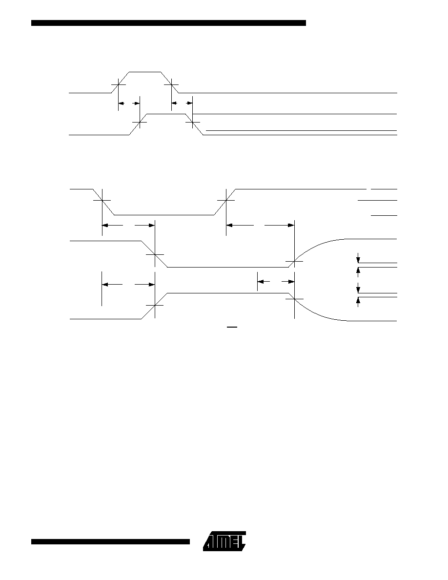
Transition
1.5 V
1.5 V
VOH
1.5 V
VOL
Output
Transition
t
PLH
t
PHL
Propagation Delay Waveforms
Control
Input
Enable
Disable
3.0 V
3.5 V
0 V
1.5 V
0 V
0.3 V
0.3 V
1.5 V
Switch Open
Switch Closed
1.5 V
Output
Switched
Low
Output
Switched
High
t
PZL
t
PZH
t
PLZ
t
PHZ
V
OL
V
OH
Note:
1. Enable and disable waveforms are the same for both xOE and xDIR inputs.
Enable and Disable Waveforms
(1)
AT16646
5-25