
4-Bit Micro-Controller With LCD Driver, 1K Word
Features
Very low current dissipation
Wide operating voltage range
Supports both Ag and Li batteries
Powerful instruction set
4-level subroutine nesting (including interrupt)
4 event driven interrupts, 2 external and 2
internal
ROM size: 1024x15 bits
RAM size: 64x4 bits
Input ports: 2 ports/8 pins (S and M)
Output port: 1 port/4 pins (P)
Pseudo serial output port (P)
Input/output ports: 2 ports/8 pins (I/OA and I/OB)
Control outputs: ALARM, LIGHT
LCD driver outputs
(can drive up to 75 LCD segments)
Mask option to select 4 LCD drive modes: static,
duplex (1/2 duty 1/2 bias, 1/3 duty 1/2 bias or 1/3
duty 1/3 bias)
Mask option permits LCD driver output pins to
be used for DC output ports; up to 25 pins are
available
Segment PLA circuit permits any layout on LCD
panel
Built-in clock generator (crystal or RC)
Built-in voltage doubler, halver, tripler
General Description
The
APU4003 is a single chip 4-bit micro-controller with
LCD drivers. It can drive up to 3 common times or 25
segments, i.e. a 75-segment LCD driver. This 4-bit
micro-controller contains a 4-bit parallel processing
ALU, 1024x15-bit program ROM, 64x4-bit data RAM,
input/output ports, alarm driver, timer, clock generator,
crystal and RC oscillator circuit, LCD driver and 79
powerful instructions in a single chip. The HALT
instruction can be used to stop all internal operations
other than timer, clock generator, crystal/RC oscillator
and LCD driver. Very low current dissipation can be
easily achieved by combining 4 kinds of interrupt
functions and HALT instruction to minimize the
operation cycle.
Block Diagram
Preliminary
1 Ver. 0.0
APU4003
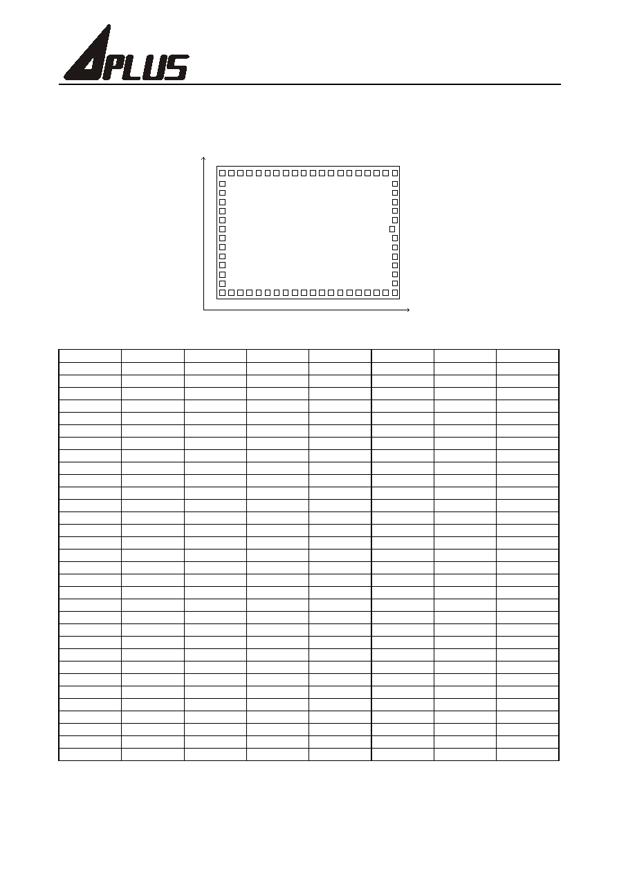
Pad Assignment
Pad open: 90 m X 90 m
Pad pitch: 160 m (Min.)
Pad Coordinates
Pad No.
Pad Name
X ( m)
Y ( m)
Pad No.
Pad Name
X ( m)
Y ( m)
1
VDD
3118
1010
33
OSCIN
50
1170
2
GND
3087
1170
34
CAP
50
1010
3
VSS1
3113
1330
35
OSCOUT
50
850
4
VSSO
3118
1490
36
COM1
50
690
5
VSS2
3118
1650
37
SEG1
50
530
6
ALARM
3118
1810
38
SEG2
50
370
7
LIGHT
3118
1970
39
SEG3
50
210
8
S4
3118
2196
40
SEG4
50
50
9
S3
2935
2196
41
SEG5
210
50
10
IOA1
2775
2196
42
SEG6
370
50
11
IOA2
2615
2196
43
SEG7
530
50
12
IOA3
2455
2196
44
SEG8
690
50
13
IOA4
2295
2196
45
SEG9
850
50
14
IOB1
2135
2196
46
SEG10
1010
50
15
IOB2
1975
2196
47
SEG11
1170
50
16
IOB3
1815
2196
48
SEG12
1330
50
17
IOB4
1655
2196
49
SEG13
1490
50
18
RESET
1495
2196
50
SEG14
1650
50
19
INT
1335
2196
51
SEG15
1810
50
20
P1
1175
2196
52
SEG16
1970
50
21
P2
1015
2196
53
SEG17
2130
50
22
P3
855
2196
54
SEG18
2290
50
23
P4
695
2196
55
SEG19
2450
50
24
M1
535
2196
56
SEG20
2610
50
25
M2
375
2196
57
SEG21
2770
50
26
M3
215
2196
58
SEG22
2930
50
27
M3
50
2196
59
SEG23
3118
50
28
TESTA
50
1970
60
SEG24
3118
210
29
CUP1
50
1810
61
SEG25
3118
370
30
CUP2
50
1650
62
COM3
3118
530
31
S2
50
1490
63
COM2
3118
690
32
S1
50
1330
64
VSS3
3118
850
* Note: The substrate must connect to VDD.
Preliminary
2 Ver. 0.0
APU4003
APU4003
Pin Description
Pin Name
Type
Description
OSCIN
OSCOUT
I
O
Typical 32.768kHz crystal is connected across OSCIN/OSCOUT for Oscillation; R/C
oscillation mode also available.
CAP
I
Connected to OSCOUT for compensation capacitor.
S1~4
I
Port for input only with chattering eliminator for CK10 (32ms), CK8 (8ms) & CK6
(2ms). (PLA mask option).
M1~4
I
Input ports.
P1~4
O
Output ports.
IOA1~4
I/O
Input/Output ports. After power-on reset, sets as input mode.
IOB1~4
I/O
Input/Output ports. After power-on reset, sets as input mode.
INT
I
External interrupt request control input pin.
RESET
I
System reset pin.
LIGHT
O
Output only for outputting signal to drive transistor for light.
ALARM
O
Output only for outputting 4kHz/2kHz/1kHz modulation signal. Also can be used to
output a non-modulation signal.
VDD
(+)Power supply pin.
GND
Power supply pin for logic unit inside LSI. When using Li version, a capacitor must be
connected across GND and VDD to prevent the logic unit from malfunctioning.
VSS0
VSS1
VSS2
VSS3
(--) Power supply pin.
* For Ag version, apply (--) side to both VSS0 & VSS1.
For other than Ag version, apply (--) side to both VSS0 & VSS2.
LCD power supply pin.
CUP1~2
O
Pins for connecting the voltage step-up (step-down) capacitor.
COM1~3
O
Output pins for LCD panel common plate.
The following pin is used in each case.
Statuc
1/2 duty 1/3 duty
COM1
COM2
COM3
Alternating Frequency
0
32Hz*
0
0
32Hz*
0
0
0
43Hz*
* Frequency can be doubled, quadrupled with PLA.
SEG1~25
O
Output pins for LCD panel segments.
* Also used as output ports with mask option.
TESTA
*
Test pin (for internal testing only).
Absolute Maximum Rating
Ta = 0 to 70 , VDD=0V
Name
Symbol
Rating
Unit
V
SS1
-5.5 ~ +0.3
V
V
SS2
-5.5 ~ +0.3
V
Maximum Supply Voltage
V
SS3
-8.5 ~ +0.3
V
V
IN1
V
SS1
-0.3 to +0.3
V
Maximum Input Voltage
V
IN2
V
SS2
-0.3 to +0.3
V
V
OUT1
V
SS1
-0.3 to +0.3
V
V
OUT2
V
SS2
-0.3 to +0.3
V
Maximum Output Voltage
V
OUT3
V
SS3
-0.3 to +0.3
V
Maximum Operating Temperature
t
OPG
0 to +70
Maximum Storage Temperature
t
STG
-25 to +125
Preliminary
3 Ver. 0.0
APU4003

Allowable Operating Conditions
Ta = 0 to 70 , V
DD
=0V
Name
Symbol
Condition
Min.
Max.
Unit
V
SS1
-5.25
-1.7
V
V
SS2
-5.25
-3.5
V
Supply Voltage
V
SS3
External RC Mode
-8.0
-3.5
V
V
SS1
-5.25
-1.2
V
V
SS2
-5.25
-2.4
V
Supply Voltage
V
SS3
Crystal Mode
-8.0
-2.4
V
V
SS1
-1.35
V
Oscillator Start-up Supply Voltage
V
SS2
Crystal Mode
-2.4
V
Input H Voltage
V
IH1
0.3V
SS1
0
V
Input L Voltage
V
IL1
Ag Battery Mode
V
SS1
0.7V
SS1
V
Input H Voltage
V
IH2
0.3V
SS2
0
V
Input L Voltage
V
IL2
Li Battery Mode
V
SS2
0.7V
SS2
V
Input H Voltage
V
IH3
0.3V
SS1
0
V
Input L Voltage
V
IL3
OSCIN at Ext. RC & Ag
Battery Mode
V
SS1
0.8V
SS1
V
Input H Voltage
V
IH4
0.2V
SS2
0
V
Input L Voltage
V
IL4
OSCIN at Ext. RC & Li Battery
Mode
V
SS2
0.8V
SS2
V
f
OPG1
Ag Battery Mode
32
32
kHz
f
OPG2
Li Battery Mode
32
100
kHz
Operating Freq.
f
OPG3
External RC Mode
32
1000
kHz
Electrical Characteristics
Ta=0 to 70 , VDD=0V
Input resistance
Name
Symbol
Condition
Min.
Typ.
Max.
Unit
R
IIH1
V
I
=0.8V
SS1
, #1
10
40
100
k
R
IIH2
V
I
=0.8V
SS2
, #2
10
40
100
k
L -Level Hold t
R
R
IIH3
V
I
=0.8V
SS2
, #3
5
20
50
k
R
MSD1
V
I
=V
DD
, #1
200
500
1000
k
R
MSD2
V
I
=V
DD
, #2
200
500
1000
k
M/S Pull-Down t
R
R
MSD3
V
I
=V
DD
, #3
100
250
500
k
R
INTU1
V
I
=V
SS1
, #1
200
500
1000
k
R
INTU2
V
I
=V
SS2
, #2
200
500
1000
k
INT Pull-Up t
R
R
INTU3
V
I
=V
SS2
, #3
100
250
500
k
R
INTD1
V
I
=V
DD
, #1
200
500
1000
k
R
INTD2
V
I
=V
DD
, #2
200
500
1000
k
INT Pull-Down t
R
R
INTD3
V
I
=V
DD
, #3
100
250
500
k
R
MSD1
V
I
=V
DD
or V
SS1
, #1
5
20
50
k
R
MSD2
V
I
=V
DD
or V
SS2
, #2
5
20
50
k
RES Pull-Down t
R
R
MSD3
V
I
=V
DD
or V
SS2
, #3
5
20
50
k
Note: #1: V
SS1
= -1.2V ( Ag ), #2: V
SS2
= -2.4V ( Li ), #3: V
SS2
= -4V (ExtV).
Preliminary
4 Ver. 0.0
APU4003
DC output characteristics
Name
Symbol
Condition
For
Min.
Typ.
Max.
Unit
V
OH1a
I
OH
=-200 A, #1
-0.5
-0.3
-0.1
V
V
OH2 a
I
OH
=-1mA, #2
-1
-0.6
-0.3
V
Output H Voltage
V
OH3 a
I
OH
=-3mA, #3
Alarm
Light
-1.5
-1.0
-0.5
V
V
OL1 a
I
OL
=400 A, #1
-1.1
-0.9
-0.7
V
V
OL2 a
I
OL
=2mA, #2
-2.1
-1.8
-1.4
V
Output L Voltage
V
OL3 a
I
OL
=6mA, #3
-3.5
-3.0
-2.5
V
V
OH1b
I
OH
=-100 A, #1
-0.5
-0.3
-0.1
V
V
OH2b
I
OH
=-500 A, #2
-1
-0.6
-0.3
V
Output H Voltage
V
OH3b
I
OH
=-1.5mA, #3
-1.5
-1.0
-0.5
V
V
OL1b
I
OL
=200 A, #1
-1.1
-0.9
-0.7
V
V
OL2b
I
OL
=1mA, #2
-2.1
-1.8
-1.4
V
Output L Voltage
V
OL3b
I
OL
=3mA, #3
P port
IOA-n
IOB-n
-3.5
-3.0
-2.5
V
Note: #1: V
SS1
= -1.2V ( Ag ), #2: V
SS2
= -2.4V ( Li ), #3: V
SS2
= -4V (ExtV).
Segment driver output characteristics
Name
Symbol
Condition
For
Min.
Typ.
Max.
Unit
CMOS output mode
V
OH1c
I
OH
=-10 A, #1
-0.5
-0.3
-0.1
V
V
OH2c
I
OH
=-50 A, #2
-1
-0.6
-0.3
V
Output H Voltage
V
OH3c
I
OH
=-200 A, #3
-1.5
-1.0
-0.5
V
V
OL1c
I
OL
=20 A, #1
-1.1
-0.9
-0.7
V
V
OL2c
I
OL
=100 A, #2
-2.1
-1.8
-1.4
V
Output L Voltage
V
OL3c
I
OL
=400 A, #3
SEG-n
-3.5
-3.0
-2.5
V
Static display mode
V
OH1d
I
OH
=-1 A, #1
-0.2
V
V
OH2d
I
OH
=-1 A, #2
-0.2
V
Output H Voltage
V
OH3d
I
OH
=-1 A, #3
-0.2
V
V
OL1d
I
OL
=1 A, #1
-1.0
V
V
OL2d
I
OL
=1 A, #2
-2.2
V
Output L Voltage
V
OL3d
I
OL
=1 A, #3
SEG-n
-3.8
V
V
OH1e
I
OH
=-10 A, #1
-0.2
V
V
OH2e
I
OH
=-10 A, #2
-0.2
V
Output H Voltage
V
OH3e
I
OH
=-10 A, #3
-0.2
V
V
OL1e
I
OL
=10 A, #1
-1.0
V
V
OL2e
I
OL
=10 A, #2
-2.2
V
Output L Voltage
V
OL3e
I
OL
=10 A, #3
COM-n
-3.8
V
Duplex (1/2 bias, 1/2 duty) display mode
V
OH12f
I
OH
=-1 A, #1, #2
-0.2
V
Output H Voltage
V
OH3f
I
OH
=-1 A, #3
-0.2
V
V
OL12f
I
OL
=1 A, #1, #2
-2.2
V
Output L Voltage
V
OL3f
I
OL
=1 A, #3
SEG-n
-3.8
V
Preliminary
5 Ver. 0.0
APU4003