
07/01
D1 Package
FEATURES
·
2.5 Gb/s Differential Output TIA
·
Low Group Delay
·
Single +5V Power Supply
·
Small Size: 0.864mm x 1.014mm
·
300mW (typ) Power Dissipation
APPLICATIONS
·
SONET/SDH OC-48/STM-16
·
2.5Gb/s DWDM
·
Fiber optic receivers, transceivers and
transponders
PRODUCT DESCRIPTION
Figure 1: Circuit Block Diagram
The Anadigics ATA7550D1 is a high-speed 5V
transimpedance amplifier (TIA) available in bare die
form and manufactured using an InGaP based HBT
process. The device is used in conjunction with a
photodetector to convert an optical signal into a
differential output voltage. With its low group delay,
the ATA7550 is ideally suited for DWDM applications.
V
OUT
V
OUT
V
CC
C
EXT
V
BIAS
I
IN
GND
GND
GND
GND
GND
C
EXT
V
OUT
V
OUT
I
IN
V
CC
ATA7550
5.0V 2.5 Gb/s TIA
PRELIMINARY DATA SHEET - Rev 0

2
ATA7550
PRELIMINARY DATA SHEET - Rev 0
07/01
Table 1: Pad Description
Figure 2: Die Size and Layout
D
A
P
N
O
I
T
P
I
R
C
S
E
D
T
N
E
M
M
O
C
V
C
C
e
g
a
tl
o
V
y
l
p
p
u
S
e
v
it
i
s
o
P
V
0
.
5
+
I
N
I
t
u
p
n
I
A
I
T
t
u
p
n
i
t
n
e
rr
u
c
o
t
o
h
P
C
T
X
E
r
o
ti
c
a
p
a
C
l
a
n
r
e
t
x
e
n
a
r
o
f
n
o
it
c
e
n
n
o
C
ff
o
t
u
c
y
c
n
e
u
q
e
rf
w
o
l
e
h
t
s
t
e
S
V
T
U
O
)
d
e
tr
e
v
n
i-
n
o
N
(
e
g
a
tl
o
V
t
u
p
t
u
O
A
I
T
t
u
p
n
i
l
a
c
it
p
o
h
ti
w
'
1
'
l
a
c
i
g
o
L
V
T
U
O
)
d
e
tr
e
v
n
i(
e
g
a
tl
o
V
t
u
p
t
u
O
A
I
T
t
u
p
n
i
l
a
c
it
p
o
h
ti
w
'
0
'
l
a
c
i
g
o
L
225
µ
m
225
µ
m
GND
GND
GND
GND
GND
C
EXT
V
OUT
V
OUT
I
IN
V
CC
Die Size: 864
µ
m x 1014
µ
m
Pad Size: 100
µ
m x 100
µ
m
Pad Pitch: 150
µ
m unless
Die Thickness: 178
µ
m
3
PRELIMINARY DATA SHEET - Rev 0
07/01
ATA7550
V
C
C
V
0
.
7
I
N
I
p
p
A
m
3
T
S
C
°
5
2
1
o
t
C
°
5
6
-
p
m
e
T
e
g
a
r
o
t
S
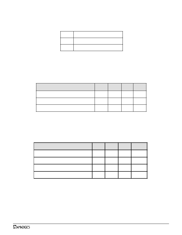
Table 2: Absolute Maximum Ratings
Table 3: Recommended Operating Conditions
Table 4: DC Electrical Specifications
1. Defined at the interface between the die and the substrate.
ELECTRICAL CHARACTERISTICS
R
E
T
E
M
A
R
A
P
N
I
M
P
Y
T
X
A
M
T
I
N
U
e
g
n
a
R
e
g
a
tl
o
V
g
n
it
a
r
e
p
O
5
7
.
4
+
0
.
5
+
5
2
.
5
+
V
e
g
n
a
R
e
r
u
t
a
r
e
p
m
e
T
g
n
it
a
r
e
p
O
)
1
(
0
1
-
0
7
O
C
e
r
u
t
a
r
e
p
m
e
T
h
c
a
tt
A
e
i
D
0
6
2
O
C
R
E
T
E
M
A
R
A
P
N
I
M
P
Y
T
X
A
M
T
I
N
U
e
g
a
tl
o
V
t
e
s
ff
O
t
u
p
n
I
6
.
2
V
e
g
a
tl
o
V
t
e
s
ff
O
t
u
p
t
u
O
5
.
3
V
t
n
e
rr
u
C
y
l
p
p
u
S
0
6
0
8
A
m
n
o
it
a
p
i
s
s
i
D
r
e
w
o
P
0
0
3
0
2
4
W
m
Stresses in excess of the absolute ratings
may cause permanent damage. Functional
operation is not implied under these
conditions. Exposure to absolute ratings
for extended periods of time may
adversely affect reliability.
The device may be operated safely over these conditions; however,
parametric performance is guaranteed only over the conditions defined in
the electrical specifications.

4
ATA7550
PRELIMINARY DATA SHEET - Rev 0
07/01
Table 5: AC Electrical Specifications
(2)
Notes:
2. The specifications are based upon the use of a PIN photodetector with a responsivity
at 1310nm of 0.9A/W (typical) and a capacitance of C
DIODE
+ C
STRAY
= 0.5pF max
connected to I
IN
via a 1nH bond wire.
3. With the use of an external capacitor.
4. Measured at 10
-10
BER with a 2
23
-1 PRBS at 2.488Gb/s.
5. 1.9 GHz bandwidth.
6. Defined as 80% of the maximum output voltage.
R
E
T
E
M
A
R
A
P
N
I
M
P
Y
T
X
A
M
T
I
N
U
e
c
n
a
t
s
i
s
e
r
s
n
a
r
T
l
a
it
n
e
r
e
ff
i
D
l
a
n
g
i
S
ll
a
m
S
)
0
0
1
-
L
R
(
0
0
5
1
0
0
0
2
)
B
d
3
-(
h
t
d
i
w
d
n
a
B
0
0
6
1
0
0
9
1
z
H
M
ff
o
t
u
C
y
c
n
e
u
q
e
r
F
w
o
L
)
3
(
0
3
z
H
k
I
;
z
H
G
7
.
1
o
t
z
H
M
1
(
y
a
l
e
D
p
u
o
r
G
N
I
)
p
p
A
0
5
2
<
0
3
±
s
p
y
ti
v
it
i
s
n
e
S
l
a
c
it
p
O
)
4
(
3
2
-
m
B
d
)
S
M
R
(
t
n
e
rr
u
C
e
s
i
o
N
t
u
p
n
I
)
5
(
0
0
8
A
n
d
a
o
lr
e
v
O
l
a
c
it
p
O
)
4
(
3
-
1
-
m
B
d
s
ti
m
i
L
t
u
p
t
u
O
h
c
i
h
w
t
a
t
n
e
rr
u
C
t
u
p
n
I
)
6
(
0
5
2
A
I(
e
g
a
tl
o
V
t
u
p
t
u
O
d
e
d
n
E
-
e
l
g
n
i
S
N
I
)
p
p
A
0
2
=
5
1
0
2
p
p
V
m
e
g
a
tl
o
V
t
u
p
t
u
O
l
a
it
n
e
r
e
ff
i
D
m
u
m
i
x
a
M
0
0
5
p
p
V
m
)
z
H
G
0
1
o
t
z
H
M
1
(
s
s
o
L
n
r
u
t
e
R
t
u
p
t
u
O
0
1
B
W
m
m
m
W

5
PRELIMINARY DATA SHEET - Rev 0
07/01
ATA7550
0.0
50.0
100.0
150.0
200.0
250.0
300.0
350.0
400.0
450.0
0
200
400
600
800
1000
Input Current (uApp)
Output
V
olt
age
(mVpp)
Figure 3: External Capacitor Required for Low Frequency Cutoff
Figure 5: Eye Diagram with an Optical Input Power of -20dBm
PERFORMANCE DATA
Figure 4: Differential Output Voltage vs. Input Current
10
100
1000
10000
0
50
100
150
200
250
300
350
400
Low Frequency Cutoff (kHz)
C
ext
(pf)
10mV/Div. 100ps/Div.