
AP1603
Step-Up DC/DC Converter
This datasheet contains new product information. Anachip Corp. reserves the rights to modify the product specification without notice. No liability is assumed as a result of the use of
this product. No rights under any patent accompany the sale of the product.
Rev.1.0 Jun. 3, 2004
1/8
Features
-A Guaranteed Start-Up from less than 0.9 V.
-High Efficiency.
-Low Quiescent Current.
-Less Number of External Components needed.
-Low Ripple and Low Noise.
-Space Saving Pb-Free Packages: SOT23-6
Applications
-Pagers.
-Cameras.
-Wireless Microphones.
-Pocket Organizers.
-Battery Backup Suppliers.
-Portable Instruments.
General Description
The AP1603 is a high efficiency step-up DC/DC
converter for applications using 1 to 2 NiMH battery
cells. Only three external components are required
to deliver a fixed output voltage of 3.3V. The
AP1603 starts up from less than 0.9V input with
1mA load. Pulse Frequency Modulation scheme
brings optimized performance for applications with
light output loading and low input voltages. The
output ripple and noise are lower compared with the
circuits operating in PSM mode.
The PFM control circuit operating in 150KHz (max.)
switching rate results in smaller passive
components. The space saving SOT23-6 packages
make the AP1603 an ideal choice of DC/DC
converter for space conscious applications, like
pagers, electronic cameras, and wireless
microphones.
Pin Assignments
1
2
3
74
6
LX
GND
OUT
REF
SOT23-6L
AP1603
5
SHDN
FB
Pin Descriptions
Name
Description
REF
1.2V Reference Voltage. Bypass with a 0.1�F
capacitor.
OUT
Power Output. OUT provides bootstrap power
to the IC.
LX
N-Channel and P-Channel Power MOSFET
Drain
GND Ground
SHDN
Shutdown Input. Drive high (>80% of V
OUT
) for
operating mode. Drive low (<20% of V
OUT
) for
shutdown mode. Connect to OUT for normal
operation.
FB Feedback
Ordering Information
Package
AP1603
X X
Packing
Blank : Tube
A : Taping
W: SOT23-6L

AP1603
Step-Up DC/DC Converter
Anachip Corp.
www.anachip.com.tw
Rev.1.0 Jun. 3, 2004
2/8
Block Diagram
+
-
+
-
S
Q
R
F/F
TRIG
One-Shot
Q
One-Shot
Q
TRIG
Maximum
On-Time
One-Shot
Error
Amplifier
Current-Limit
Amplifier
Zero
Crossing
Amplifier
Minimum
Off-Time
One-Shot
+
-
+
-
OUT
LX
GND
FB
REF
0.1uF
22uH
0.1uF
+
47uF
+
47uF
+
SHDN
P
N
V
IN
EN
FB
Absolute Maximum Ratings
Symbol
Parameter
Rating
Unit
V
CC
Supply Voltage (OUT to GND)
-0.3 to 5.5
V
V
REF
REF to GND
-0.3 to V
OUT
+0.3 V
V
SW
Switch Voltage (LX to GND)
-0.3 to V
OUT
+0.3 V
I
OUT
Output
Current
(OUT) -0.8
to
0.2
A
I
SW
Switch
Current
(LX) -0.8
to
0.2
A
T
ST
Storage Temperature Range
-65 to +150
o
C
T
OT
Operation Temperature Range
-40 to +80
o
C
AP1603
Step-Up DC/DC Converter
Anachip Corp.
www.anachip.com.tw Rev.1.0 Jun. 3, 2004
3/8
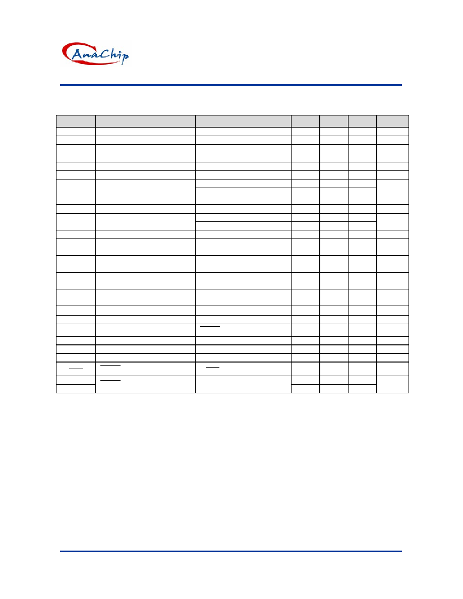
Electrical Characteristics
(V
IN
=2V, FB=V
OUT
, R
L
= , T
A
= 0�C to +85�C, unless otherwise noted. Typical values are at T
A
= +25�C.)
Symbol
Parameter
Conditions
Min.
Typ.
Max.
Unit
Minimum
Input
Voltage
- 0.9 - V
V
IN
Operating
Voltage
T
A
= +25�C
1.1
-
5.5
V
Start-Up
Voltage
T
A
= +25�C,
RL = 3k
(Note 1)
- 0.9 1.1 V
Start-Up
Voltage
Tempco
- -4 -
mV/�C
Output Voltage Range
2
-
5.5
V
FB=V
OUT
=3.3V 100
150
-
I
OUT
Steady-State Output Current
(Note2)
V
IN
=2.4V, FB=GND,
V
OUT
=5V
- 80 -
mA
V
REF
Reference
Voltage
I
REF
=0 1.196
1.22
1.244
V
FB=V
OUT
3.17
3.3
3.43
V
OUT
Output
Voltage
FB=GND
4.8 5 5.2
V
TEMPCO
Reference Voltage Tempco
-
0.05
-
mV/�C
V
REF_LOAD
Reference Voltage Load
Regulation
I
REF
=0 to 30 A
- 15 80 mV
V
REF_LINE
Reference Voltage Line
Regulation
V
IN
=1.1V to 3.6V
-
0.08
1.5
mV/V
R
DS(ON)
Internal NFET, PFET
On-Resistance
I
LX
=100mA -
0.6
1.0
I
LIM
LX Switch Current Limit
(NFET)
0.3 0.35 0.4 A
I
LEAK
LX
Leakage
Current
V
LX
=0, 5.5V; V
OUT
=5.5V -
0.05
1
A
Operating Current into OUT
V
OUT
=3.3V -
16
35
�A
Shutdown Current into OUT
SHDN
=GND
- 0.1 1 �A
Efficiency
V
OUT
=3.3V, I
LOAD
=100mA - 90 - %
t
ON
LX
Switch
On-Time
3 4 7 �s
t
OFF
LX
Switch
Off-Time
1.0 1.2 1.4 �s
I
SHDN
SHDN
Input Current
V
SHDN
=0 or V
OUT
- 0.07 50 nA
V
IL
-
-
0.2
V
IH
SHDN
Input Voltage
Based on V
OUT
Voltage
0.8 - -
V
OUT
Note 1: Start-up voltage operation is guaranteed with the addition of a Schottky 1N5819 external diode between the input and output.
Note 2: Steady-state output current indicates that the device maintains output voltage regulation under load.

AP1603
Step-Up DC/DC Converter
Anachip Corp.
www.anachip.com.tw Rev.1.0 Jun. 3, 2004
4/8
Typical Application Circuit
(1) V
OUT
=5V
SHDN
LX
OUT
REF
0.1uF
22uH
47uF
+
47uF
+
V
IN
ON
OFF
Fixed Output
( 5V )
GND
1.1V to 5.5V
FB
(2) V
OUT
=3.3V
SHDN
LX
OUT
REF
0.1uF
22uH
47uF
+
47uF
+
V
IN
ON
OFF
Fixed Output
( 3.3V )
GND
1.1V to 3.6V
FB
(3) V
OUT
=Adj
SHDN
LX
OUT
REF
0.1uF
22uH
47uF
+
47uF
+
V
IN
ON
OFF
Output
GND
1.1V to 5.5V
FB
R2
R1
V
OUT
= V
REF
(1+ )
R1
R2

AP1603
Step-Up DC/DC Converter
Anachip Corp.
www.anachip.com.tw Rev.1.0 Jun. 3, 2004
5/8
Typical Performance Characteristics
REFERENCE VOLTAGE v.s.
TEMPERATURE
1.18
1.19
1.2
1.21
1.22
1.23
-40
-20
0
20
40
60
80
TEMPERATURE (
o
C)
R
E
F
E
R
E
N
C
E VO
L
T
AG
E
(
V
)
STEADY STATE OUTPUT CURRENT
v.s.
INPUT VOLTAGE
0
80
160
240
320
400
1 1.2 1.4 1.6 1.8 2 2.2 2.4 2.6 2.8 3
INPUT VOLTAGE (V)
ST
EAD
Y STAT
E
O
U
TPU
T
CU
RR
ENT
(mA)
START-UP VOLTAGE v.s.
LOAD CURRENT
0.8
1
1.2
1.4
1.6
1.8
2
0
3
9
18
39
59
79
99
LOAD CURRENT (mA)
ST
AR
T
-
U
P
VOLTAGE (V)
with diode
without diode
1N5819
NO LOAD INPUT CURRENT v.s.
INPUT VOLTAGE
50
75
100
125
150
175
0.89
1
1.
2
1.
4
1.
6
1.
8
2
2.
2
2.
4
2.
6
2.
8
3
INPUT VOLTAGE (V)
N
O
LOAD
INPU
T
CU
RR
E
N
T
(
u
A
)