MD7101_A01
PRELIMINARY (Oct, 2003, Version 0.0)
2
AMIC Technology, Corp.
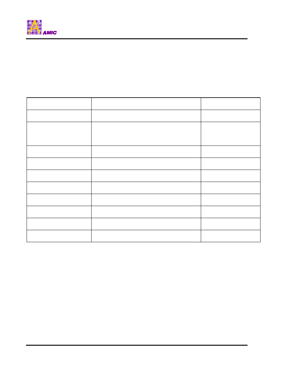
Interface
Pin Number Pin Name
Description
Note
J1-3 VIN
Supply
voltage.
J1-4
EN_REG
Voltage regulator enable input, active high (VIN).
Option.
J1-5
SPI_LATCH
Latch for SPI interface.
J1-6
SPI_CLOCK
Clock for SPI interface.
J1-7
SPI_DATA
Data for SPI interface.
J1-8 GND
Ground.
J2-1
MUTE
Receiver mute control output, active low (open drain).
Option.
J2-2
EN_AFC
AFC circuit control input, active high.
Option.
J2-3
RXDATA
Receiver data output.
MD7101_A01
PRELIMINARY (Oct, 2003, Version 0.0)
3
AMIC Technology, Corp.
Serial to Parallel Interface (SPI)
The SPI bus consists of three signals: SPI_DATA, SPI_CLOCK, and SPI_LATCH. This interface is used for external
base-band controller to communicate with internal registers. The contents of the registers are shown in the following
register description sections.
After setting SPI_LATCH signal to "Low" state, data on SPI_DATA is shifted into the internal shift register on the rising
edge of SPI_CLOCK with MSB going in first. SPI_LATCH should be asserted at the end to latch the data packet into
the register according to the address bits, bit 0 through bit 3, for each of the registers. All registers can only be written
into except the Status Register which can only be read.
When the content of the Status Register need to be fetched by external controller, external baseband controller need to
make sure that the address bits are pointing to address location 0x0 for proper read operation. After the address bits
are shifted into the SPI interface and latched by asserting SPI_LATCH, the SPI interface will be in Read Mode and the
content of the Status Register will be shifted out on SPI_DATA pin. When all 12 status bits have been shifted out, the
SPI bus will be put back to Write Mode automatically.
A. Register Description
Note: Convention used:
1: Logic level "ONE".
0: Logic level "ZERO".
X: Don't care.
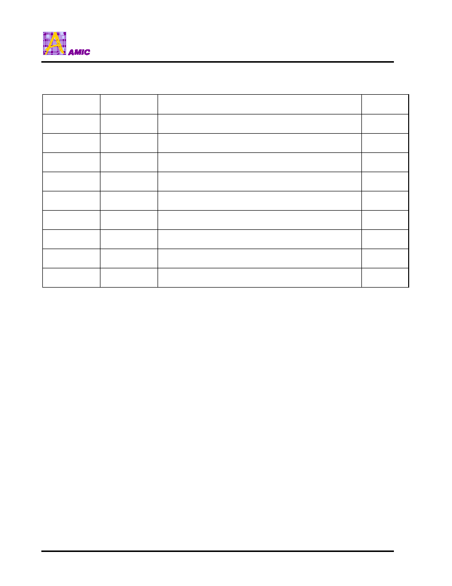
Synthesizer Configuration Register I (Write only / Address 0xf)
Bit 15 Bit 14 Bit 13 Bit12 Bit11 Bit10
Bit9
Bit8
Bit7 Bit6 Bit5 Bit4 Bit3
Bit2
Bit 1
Bit 0
MB6 MB5 MB4 MB3 MB2 MB1 MB0 MA4 MA3 MA2 MA1 MA0 1 1 1 1
Synthesizer Configuration Register II (Write only / Address 0x7)
Bit 15 Bit 14 Bit 13 Bit12 Bit11 Bit10
Bit9
Bit8
Bit7 Bit6 Bit5 Bit4 Bit3
Bit2
Bit 1
Bit 0
X MB9 MB8 MB7 R7 R6 R5 R4 R3 R2 R1 R0 0 1 1 1
Synthesizer Configuration Register I and Synthesizer Configuration Register II control synthesizer frequency settings
where
MA[4:0]: A counter[4:0] . Valid range is from 0 to 31.
MB[9:0]: B counter[9:0] . Valid range is from 0 to 1023.
R[7:0]: R counter[7:0] . Valid range is from 2 to 255,
for this module must be set to 0x78 for proper operation.
The content of A, B and R registers are in unsigned binary format (i.e., 11111
2
= 31
10
).
The equation for setting the synthesizer frequency is:
f
vco
= f
crystal
* (32*B + A) / R, (B A).
For example :
If f
vco
= 2450MHz , f
crysta
= 12MHz , f
reference
= 100KHz.
Then R = f
crysta
/ f
reference
= 120 =01111000
2
, B = 765 = 1011111101
2
, A = 20 = 10100
2
.
MD7101_A01
PRELIMINARY (Oct, 2003, Version 0.0)
4
AMIC Technology, Corp.
Crystal Control Register (Write only / Address 0xb)
Bit 15 Bit 14 Bit 13 Bit12 Bit11 Bit10
Bit9
Bit8
Bit7 Bit6 Bit5 Bit4 Bit3
Bit2
Bit 1
Bit 0
0 DP TXH2
TXH1
TXH0
TXL2
TXL1 TXL0 FX3 FX2 FX1 FX0 1
0
1
1
DP: Data Polarity. This control bit sets data output polarity.
0: Data is inverted.
1: Normal.
TXH[2:0]: Must be set to 0x0 for proper operation.
TXL[2:0]: Must be set to 0x0 for proper operation.
FX[3:0]: Must be set to 0x0 for proper operation.
VCO Control Register (Write only / Address 0x3)
Bit 15 Bit 14 Bit 13 Bit12 Bit11 Bit10
Bit9
Bit8
Bit7 Bit6 Bit5 Bit4 Bit3
Bit2
Bit 1
Bit 0
VTH2
VTH1
VTH0 T1 T0 HP0 CP2 CP1 CP0 VC2 VC1 VC0 0
0
1
1
VTH[2:0]: Set VCO tuning voltage range,
for this module must be set to 0x6 for proper operation.
0x0 = 0.3 to VDD-0.3V , 0x1 = 0.4 to VDD-0.4V ,
0x2 = 0.5 to VDD-0.5V , 0x3 = 0.6 to VDD-0.6V ,
0x4 = 0.7 to VDD-0.7V , 0x5 = 0.8 to VDD-0.8V ,
0x6 = 0.9 to VDD-0.9V , 0x7 = 1.0 to VDD-1.0V ,
T[1:0]: Reserved. Must be set to 0x0 for proper operation.
HP0: RF output power level control.
0: Low power output (-16 dBm).
1: High power output (-6 dBm).
CP[2]: Reserved. Must be set to 0x0 for proper operation.
CP[1:0]: Charge pump output current control,
for this module must be set to 0x1(300uA) for proper operation.
0x0 = 100uA , 0x1 = 300uA ,
0x2 = 500uA , 0x3 = 700uA ,
VC[2:0]: Reserved. Must be set to 0x4 for proper operation.
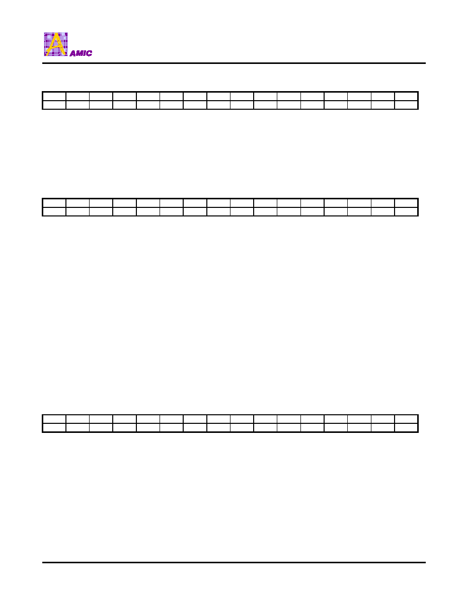
RX Control Register (Write only / Address 0xd)
Bit 15 Bit 14 Bit 13 Bit12 Bit11 Bit10
Bit9
Bit8
Bit7 Bit6 Bit5 Bit4 Bit3
Bit2
Bit 1
Bit 0
T2 T1 T0 MT2 MT1 MT0 MTC DM4 DM3 DM2 DMI DM0 1
1
0
1
T[2:0]: Reserved. Must be set to 0x0 for proper operation.
MT[2:0]: Internal voltage threshold level for mute output (pin 37).
0x0 = 0.581*VDD , 0x1 = 0.516*VDD ,
0x2 = 0.452*VDD , 0x3 = 0.387*VDD ,
0x4 = 0.323*VDD , 0x5 = 0.258*VDD ,
0x6 = 0.194*VDD , 0x7 = 0.129*VDD ,
MTC: RXDATA mute function enable.
0: Disable mute function.
1: Enable mute function. When RSSI output voltage level is higher than the threshold set by MT[2:0], RXDATA becomes
inactive and pull high.