AP160
8-BIT MICROCONTROLLER
DATA SHEET
WITH 8KB OTP
October
2001
Version 0.0
1
AMIC Technology, Inc.
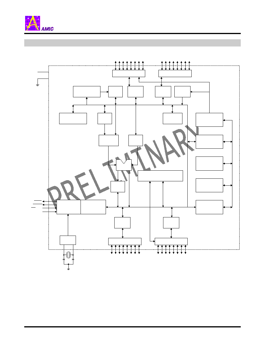
GENERAL DESCRIPTION
The AP160 is a wide operating voltage, Low power consumption and high performance with AMIC high-density CMOS
technology. All instruction set of AP160 are fully compatible with the standard 8051. The AP160 contains 8K bytes OTP
EPROM, 256 bytes RAM, four 8-bit bi-directional and bit addressable I/O ports, three 16-bit timer/counter and eight interrupt
sources. To reduce power consumption, idle mode and power down mode are provided to implementation. For data
protection, program lock bits can be performed through programming LB1, LB2 and LB3. The AMIC AP160 is a useful and
powerful microcontroller in many control system application.
FEATURES
l
Compatible with MCS-51 Products
l
256 X 8 bit internal Data RAM.
l
8KB On-Chip OTP EPROM.
l
2.7V~5.5V Operating Range.
l
Fully Static Operation : 0Hz to 16 MHz
l
0~33MHZ speed range at VCC=5V.
l
32 Programmable I/O pins
l
Three 16-Bit Timers/Counters.
l
Programmable clock out.
l
Full-duplex UART
l
Eight interrupt sources.
l
2 level priority-interrupt.
l
Power reduction control modes
n
Idle mode
n
Power-down mode
l
3 security bits.
l
Low EMI (Inhibit ALE)
l
Wake-up from Power Down by an external interrupt.
l
Available in PLCC and QFP44 packages.

AP160
Version 0.0
4
AMIC Technology, Inc.
PIN DESCRIPTIONS
SYMBOL
TYPE
DESCRIPTIONS
VSS
I
Ground.
VCC
I
Supply voltage.
P0.0-P0.7
I/O Port 0 is an 8-bit open drain, bidirectional I/O port. When 1s are written to port 0 pins, the pins
can be used as high-impedance inputs. Port 0 can also be configured to be the multiplexed
low-order address/data bus during accesses to external program and data memory. In this
mode, P0 has internal pullups. Port 0 also receives the code bytes during programming on-chip
OTP EPROM and outputs the code bytes during program verification. External pullups are
required during program verification.
P1.0-P1.7
I/O Port 1 is an 8-bit bidirectional I/O port with internal pullups. The Port 1 output buffers can
sink/source four TTL inputs. When 1s are written to Port 1 pins, they are pulled high by the
internal pullups and can be used as inputs. As inputs, Port 1 pins that are externally being
pulled low will source current (
IL
I
) because of the internal pullups. In addition, P1.0 and P1.1
can be configured to be the timer/counter 2 external count input (P1.0/T2) and the timer/counter
2 trigger input (P1.1/T2EX), respectively, as shown in the following:
T2 (P1.0): Timer/Counter 2 external count input/clockout (see Programmable Clock-Out)
T2EX (P1.1): Timer/Counter 2 Reload/Capture/Direction control.
Port 1 also receives the low-order address bytes during programming on-chip OTP EPROM
and verification.
P2.0-P2.7
I/O Port 2 is an 8-bit bidirectional I/O port with internal pullups.
The Port 2 output buffers can
sink/source four TTL inputs.
When 1s are written to Port 2 pins, they are pulled high by the
internal pullups and can be used as inputs. As inputs,
Port 2 pins that are externally being
pulled low will source
current (
IL
I
) because of the internal pullups.
Port 2 emits the high-order
address byte during fetches
from external program memory and during accesses to external
data memory that use 16-bit addresses (MOVX @DPTR). In this application, Port 2 uses strong
internal pullups
when emitting 1s. During accesses to external data memory that use 8-bit
addresses (MOVX @ RI), Port 2
emits the contents of the P2 Special Function Register. Port 2
also receives the high-order address bits and some control signals during programming on-chip
OTP EPROM and verification.
P3.0-P3.7
I/O Port 3 is an 8-bit bidirectional I/O port with internal pullups. The Port 3 output buffers can
sink/source four TTL inputs.When 1s are written to Port 3 pins, they are pulled high by the
internal pullups and can be used as inputs. As inputs, Port 3 pins that are externally being
pulled low will source current (
IL
I
) because of the pullups.
Port 3 also serves the functions of
various special features of the AP160, as shown below:
RXD (P3.0): Serial input port
TXD (P3.1): Serial output port
INT0 (P3.2): External interrupt
INT1 (P3.3): External interrupt
T0 (P3.4): Timer 0 external input
T1 (P3.5): Timer 1 external input
WR (P3.6): External data memory write strobe
RD (P3.7): External data memory read strobe
Port 3 also receives some control signals for programming and verification.
RST
I
Reset input. A high on this pin for two machine cycles while the oscillator is running resets the
device.

AP160
Version 0.0
5
AMIC Technology, Inc.
SYMBOL
TYPE
DESCRIPTIONS
ALE/PROG
O/I Address Latch Enable is an output pulse for latching the low byte of the address during
accesses to external memory. This pin is also the program pulse input (PROG) during
Programming on-chip OPT EPROM. In normal operation, ALE is emitted at a constant rate of
1/6 the oscillator frequency and may be used for external timing or clocking purposes. Note,
however, that one ALE pulse is skipped during each access to external data memory. If
desired, ALE operation can be disabled by setting bit 0 of SFR location 8EH. With the bit set,
ALE is active only during a MOVX or MOVC instruction. Otherwise, the pin is weakly pulled
high. Setting the ALE-disable bit has no effect if the microcontroller is in external execution
mode.
PSEN
O
Program Store Enable is the read strobe to external program memory. When the AP160 is
executing code from external program memory, PSEN is activated twice each machine cycle,
except that two PSEN activations are skipped during each access to external data memory.
EA/Vpp
I
External Access Enable. EA must be strapped to GND in order to enable the device to fetch
code from external program memory locations starting at 0000H up to FFFFH. Note, however,
that if lock bit 1 is programmed, EA will be internally latched on reset. EA should be strapped to
VCC for internal program executions. This pin also receives the 12-volt programming enable
voltage (VPP) during programming OTP EPROM.
XTAL1
I
Input to the inverting oscillator amplifier and input to the internal clock operating circuit.
XTAL2
O
Output from the inverting oscillator amplifier.