
Publication Number 31136 Revision A Amendment 1 Issue Date February 5, 2004
PRELIMINARY
S71NS128JA0/S71NS064JA0
Stacked Multi-Chip Product (MCP)
128 Megabit (8 M x 16-Bit) and 64 Megabit (4 M x 16-Bit),
110 nm CMOS 1.8 Volt-only Simultaneous Read/Write,
Burst Mode Flash Memories with 16 Megabit (1M x 16-Bit) pSRAM
Distinctive Characteristics
Single 1.8 volt read, program and erase (1.7
to 1.95 volt)
Multiplexed Data and Address for reduced
I/O count
-- A15A0 multiplexed as DQ15DQ0
-- Addresses are latched by AVD# control input when
CE# low
Simultaneous Read/Write operation
-- Data can be continuously read from one bank while
executing erase/program functions in other bank
-- Zero latency between read and write operations
Read access times at 66/54 MHz (C
L
=30 pF)
-- Burst access times of 11/13.5 ns
at industrial temperature range
-- Asynchronous random access times
of 65/70 ns
-- Synchronous random access times
of 71/87.5 ns
Burst length
-- Continuous linear burst
-- 8/16/32 word linear burst with wrap around
-- 8/16/32 word linear burst without wrap around
Power dissipation (typical values, 8 bits
switching, C
L
= 30 pF)
-- Burst Mode Read: 25 mA
-- Simultaneous Operation: 40 mA
-- Program/Erase: 15 mA
-- Standby mode: 9 µA
Sector Architecture
-- Four 8 Kword sectors
-- Two hundred fifty-five (S29NS128J) or one hundred
twenty-seven (S29NS064J) 32 Kword sectors
-- Four banks
Sector Protection
-- Software command sector locking
-- All sectors locked when V
PP
= V
IL
Handshaking feature
-- Provides host system with minimum possible latency
by monitoring RDY
Supports Common Flash Memory
Interface (CFI)
Software command set compatible with
JEDEC 42.4 standards
-- Backwards compatible with Am29F and Am29LV
families
Manufactured on 110 nm process technology
Minimum 100,000 erase cycle guarantee
per sector
20-year data retention
-- Reliable operation for the life of the system
Embedded Algorithms
-- Embedded Erase algorithm automatically
preprograms and erases the entire chip or any
combination of designated sectors
-- Embedded Program algorithm automatically writes
and verifies data at specified addresses
Data# Polling and toggle bits
-- Provides a software method of detecting program and
erase operation completion
Erase Suspend/Resume
-- Suspends an erase operation to read data from, or
program data to, a sector that is not being erased,
then resumes the erase operation
Hardware reset input (RESET#)
-- Hardware method to reset the device for reading
array data
CMOS compatible inputs and outputs
Package
-- 48-ball Very Thin FBGA (S71NS128JA0)
-- 44-ball Very Thin FBGA (S71NS064JA0)

2
S71NS128JA0/S71NS064JA0
31136A1 February 5, 2004
P r e l i m i n a r y
PRODUCT SELECTOR GUIDE
Part Number
S71NS128JA0, S71NS064JA0
MCP Model Number
00, 10, 20
01, 11, 21
Burst Frequency
66 MHz
54 MHz
Fl
a
s
h Me
mo
r
y
Flash Memory Device/Model Number
S29NS128J/00,
S29NS064J/00
Flash Speed Option
0P
0L
Max Initial Synchronous Access Time, ns (t
IACC
)
71
87.5
Max Burst Access Time, ns (t
BACC
)
11
13.5
Max Asynchronous Access Time, ns (t
ACC
)
65
70
Max CE# Access Time, ns (t
CE
)
Max OE# Access Time, ns (t
OE
)
11
13.5
pS
RAM
Max Access Time, ns (t
ACC2
)
90
90
Max CE# Access Time, ns (t
ACC3
)
90
90
Max OE# Access Time, ns (t
OE
)
50
50

February 5, 2004 31136A1
S71NS128JA0/S71NS064JA0
3
P r e l i m i n a r y
MCP Block Diagram
1. A15A0 are multiplexed with DQ15DQ0.
2. A
MAX
indicates the highest order address bit.
Flash
Memory
(S29NS128J
or
S29NS064J)
RESET#
V
PP
CE#
OE#
WE#
AVD#
16 Mb
pSRAM
RDY
CLK
A19-A16
A20
A21
A21/LB#
LB#
* A22/UB#
UB#
CS#
A/DQ15-A/DQ0
A22
* Note: A22 available for 128 Mb Flash only

4
S71NS128JA0/S71NS064JA0
31136A1 February 5, 2004
P r e l i m i n a r y
Connection Diagram
A1
RDY
A2
A21/LB#
A3
GND
A4
CLK
A5
V
CC
A6
WE#
A7
V
PP
A8
A19
A9
A17
A10
A22/UB#
B1
V
CC
B2
A16
B3
A20
B4
AVD#
B5
NC
B6
RESET#
B7
CS#
B8
A18
B9
CE#
B10
GND
C1
GND
C2
A/DQ7
C3
A/DQ6
C4
A/DQ13
C5
A/DQ12
C6
A/DQ3
C7
A/DQ2
C8
A/DQ9
C9
A/DQ8
C10
OE#
D1
A/DQ15
D2
A/DQ14
D3
GND
D4
A/DQ5
D5
A/DQ4
D6
A/DQ11
D7
A/DQ10
D8
V
CC
D9
A/DQ1
D10
A/DQ0
NC
NC
NC
NC
NC
NC
NC
NC
S71NS128JA0
48-Ball Very Thin FBGA (NLA048)
Top View, Balls Facing Down

February 5, 2004 31136A1
S71NS128JA0/S71NS064JA0
5
P r e l i m i n a r y
CONNECTION DIAGRAM
A1
RDY
A2
A21/LB#
A3
GND
A4
CLK
A5
V
CC
A6
WE#
A7
V
PP
A8
A19
A9
A17
A10
UB#
B1
V
CC
B2
A16
B3
A20
B4
AVD#
B5
NC
B6
RESET#
B7
CS#
B8
A18
B9
CE#
B10
GND
C1
GND
C2
A/DQ7
C3
A/DQ6
C4
A/DQ13
C5
A/DQ12
C6
A/DQ3
C7
A/DQ2
C8
A/DQ9
C9
A/DQ8
C10
OE#
D1
A/DQ15
D2
A/DQ14
D3
GND
D4
A/DQ5
D5
A/DQ4
D6
A/DQ11
D7
A/DQ10
D8
V
CC
D9
A/DQ1
D10
A/DQ0
NC
NC
NC
NC
S71NS064JA0
44-Ball Very Thin FBGA (NLB044)
Top View, Balls Facing Down

6
S71NS128JA0/S71NS064JA0
31136A1 February 5, 2004
P r e l i m i n a r y
Input/Output Descriptions
A22/UB#
=
Address Inputs, pSRAM Upper Byte Control (A22 available
for 128 Mb Flash)
A21/LB#
=
Address Inputs, pSRAM Lower Byte Control
A20A16
=
Address Inputs
A/DQ15A/DQ0
=
Multiplexed Address/Data input/output
CS#
=
pSRAM Chip Select Input
CE#
=
Flash Chip Enable Input. Asynchronous relative to CLK for
the Burst mode.
OE#
=
Output Enable Input. Asynchronous relative to CLK for the
Burst mode.
WE#
=
Write Enable Input.
V
CC
=
Device Power Supply (1.7 V1.95 V).
GND
=
Ground
NC
=
No Connect; not connected internally
RDY
=
Ready output; indicates the status of the Burst read.
V
OL
= data invalid.
CLK
=
Flash Clock input. The first rising edge of CLK in conjunction
with AVD# low latches address input and activates burst
mode operation. After the initial word is output, subsequent
rising edges of CLK increment the internal address counter.
CLK should remain low during asynchronous access.
AVD#
=
Address Valid input. Indicates to device that the valid
address is present on the address inputs (address bits A15
A0 are multiplexed, address bits A22A16 are address
only).
V
IL
= for asynchronous mode, indicates valid address; for
burst mode, causes starting address to be latched on rising
edge of CLK.
V
IH
= device ignores address inputs
RESET#
=
Hardware reset input. V
IL
= device resets and returns to
reading array data
V
PP
=
At 12 V, accelerates programming; automatically places
device in unlock bypass mode. At V
IL
, disables program and
erase functions. Should be at V
IH
for all other conditions.
Logic Symbol
16
A/DQ15
A/DQ0
A20A16
CE#
OE#
WE#
RESET#
CLK
RDY
AVD#
CS#
V
PP
*A22 available for 128Mb Flash only.
A21/LB#
*A22/UB#

February 5, 2004 31136A1
S71NS128JA0/S71NS064JA0
7
P r e l i m i n a r y
ORDERING INFORMATION
The order number (Valid Combination) is formed by the following:
Valid Combinations
The following configurations are planned to be supported for this device. Consult the local
sales office to confirm availability of specific valid combinations and to check on newly re-
leased combinations.
S71NS
128
J
A0
BA
W
00
3
PACKING TYPE
3
= 13 inch Tape and Reel
ADDITIONAL ORDERING OPTIONS
00
= 66 MHz Flash,EMLSI pSRAM
01
= 54 MHz Flash,EMLSI pSRAM
10
= 66 MHz Flash,Cypress pSRAM
11
= 54 MHz Flash,Cypress pSRAM
20
= 66 MHz Flash,Micron pSRAM
21
= 54 MHz Flash,Micron pSRAM
TEMPERATURE RANGE
W
= Wireless (25
°
C to +85
°
C)
For Industrial (40
°
C to +85
°
C), contact local
sales office
PACKAGE TYPE
BA
=
Very Thin Fine-Pitch BGA
Lead (Pb)-Free Compliant Package
BF
=
Very Thin Fine-Pitch BGA
Lead (Pb)-Free Package
pSRAM DENSITY
A0
= 16 Megabit (1M x 16-Bit)
FLASH PROCESS TECHNOLOGY
J
= 110 nm Floating Gate Technology
FLASH DENSITY
128
= 128 Megabit (8 M x 16-Bit)
064
= 64 Megabit (4 M x 16-Bit)
DEVICE FAMILY
S71NS = Stacked Multi-Chip Product,
Simultaneous Read/Write, Burst Mode Flash Memory with Multiplexed I/O
1.8-Volt Operation, Top Boot Sectors, and pSRAM

8
S71NS128JA0/S71NS064JA0
31136A1 February 5, 2004
P r e l i m i n a r y
Valid Combinations for BGA Package
Order Number
Package Marking
Package
Density
Speed
S71NS128JA0BAW013
71NS128JA0BAW01
Pb-Free Compliant
128 Mb + 16 Mb EMLSI
pSRAM
54 MHz
S71NS128JA0BFW013
71NS128JA0BFW01
Pb-Free
S71NS128JA0BAW113
71NS128JA0BAW11
Pb-Free Compliant
128 Mb + 16 Mb Cypress
pSRAM
S71NS128JA0BFW113
71NS128JA0BFW11
Pb-Free
S71NS128JA0BAW213
71NS128JA0BAW21
Pb-Free Compliant
128 Mb + 16 Mb Micron
pSRAM
S71NS128JA0BFW213
71NS128JF0BAW21
Pb-Free
S71NS064JA0BAW013
71NS064JA0BAW01
Pb-Free Compliant
64 Mb + 16 Mb EMLSI
pSRAM
S71NS064JA0BFW013
71NS064JA0BFW01
Pb-Free
S71NS064JA0BAW113
71NS064JA0BAW11
Pb-Free Compliant
128 Mb + 16 Mb Cypress
pSRAM
S71NS064JA0BFW113
71NS064JA0BFW11
Pb-Free
S71NS064JA0BAW213
71NS064JA0BAW21
Pb-Free Compliant
128 Mb + 16 Mb Micron
pSRAM
S71NS064JA0BFW213
71NS064JF0BAW21
Pb-Free

February 5, 2004 31136A1
S71NS128JA0/S71NS064JA0
9
P r e l i m i n a r y
PHYSICAL DIMENSIONSS71NS128JA0
NLA048
--
48
-Ball Very Thin Fine-Pitch Ball Grid Array (FBGA)
10 x 11
mm Package
* For reference only. BSC is an ANSI standard for Basic Space Centering
PACKAGE
NLA 048
JEDEC
N/A
9.95 mm x 10.95 mm NOM
NOTE
PACKAGE
SYMBOL
MIN
NOM
MAX
A
1.05
---
1.20
OVERALL THICKNESS
A1
0.20
---
---
BALL HEIGHT
A2
0.85
0.91
0.97
BODY THICKNESS
D
9.85
9.95
10.05
BODY SIZE
E
10.85
10.95
11.05
BODY SIZE
D1
4.50 BSC.
BALL FOOTPRINT
E1
1.50 BSC.
BALL FOOTPRINT
MD
10
ROW MATRIX SIZE D DIRECTION
ME
4
ROW MATRIX SIZE E DIRECTION
N
48
TOTAL BALL COUNT
b
0.25
0.30
0.35
BALL DIAMETER
e
0.50 BSC.
BALL PITCH
SD / SE
0.25 BSC.
SOLDER BALL PLACEMENT
---
DEPOPULATED SOLDER BALLS
3297 \ 16-038.22a1
NOTES:
1. DIMENSIONING AND TOLERANCING PER ASME Y14.5M-1994.
2. ALL DIMENSIONS ARE IN MILLIMETERS.
3. BALL POSITION DESIGNATION PER JESD 95-1, SPP-010 (EXCEPT
AS NOTED).
4. e REPRESENTS THE SOLDER BALL GRID PITCH.
5. SYMBOL "MD" IS THE BALL ROW MATRIX SIZE IN THE
"D" DIRECTION.
SYMBOL "ME" IS THE BALL COLUMN MATRIX SIZE IN THE
"E" DIRECTION.
N IS THE TOTAL NUMBER OF SOLDER BALLS.
6
DIMENSION "b" IS MEASURED AT THE MAXIMUM BALL
DIAMETER IN A PLANE PARALLEL TO DATUM C.
7
SD AND SE ARE MEASURED WITH RESPECT TO DATUMS
A AND B AND DEFINE THE POSITION OF THE CENTER
SOLDER BALL IN THE OUTER ROW.
WHEN THERE IS AN ODD NUMBER OF SOLDER BALLS IN
THE OUTER ROW PARALLEL TO THE D OR E DIMENSION,
RESPECTIVELY, SD OR SE = 0.000.
WHEN THERE IS AN EVEN NUMBER OF SOLDER BALLS IN
THE OUTER ROW, SD OR SE = e/2
8. NOT USED.
9. "+" INDICATES THE THEORETICAL CENTER OF DEPOPULATED
BALLS.
10 A1 CORNER TO BE IDENTIFIED BY CHAMFER, LASER OR INK
MARK, METALLIZED MARK INDENTATION OR OTHER MEANS.
TOP VIEW
BOTTOM VIEW
SIDE VIEW
INDEX MARK
A1 CORNER
NF4
NF1
NF8
1
2
4
3
5
6
8
9
7
NF2
NF3
A
B
NF7
NF5
C
D
10
NF6
D
A
10
E
A1 CORNER
SE
7
E1
D1
e
1.00
1.00
7
SD
B
6
b
C
M
C
M
0.15
0.05
A
1.00
1.00
C
0.10
C
0.08
A
B
C
A2
SEATING PLANE
A1
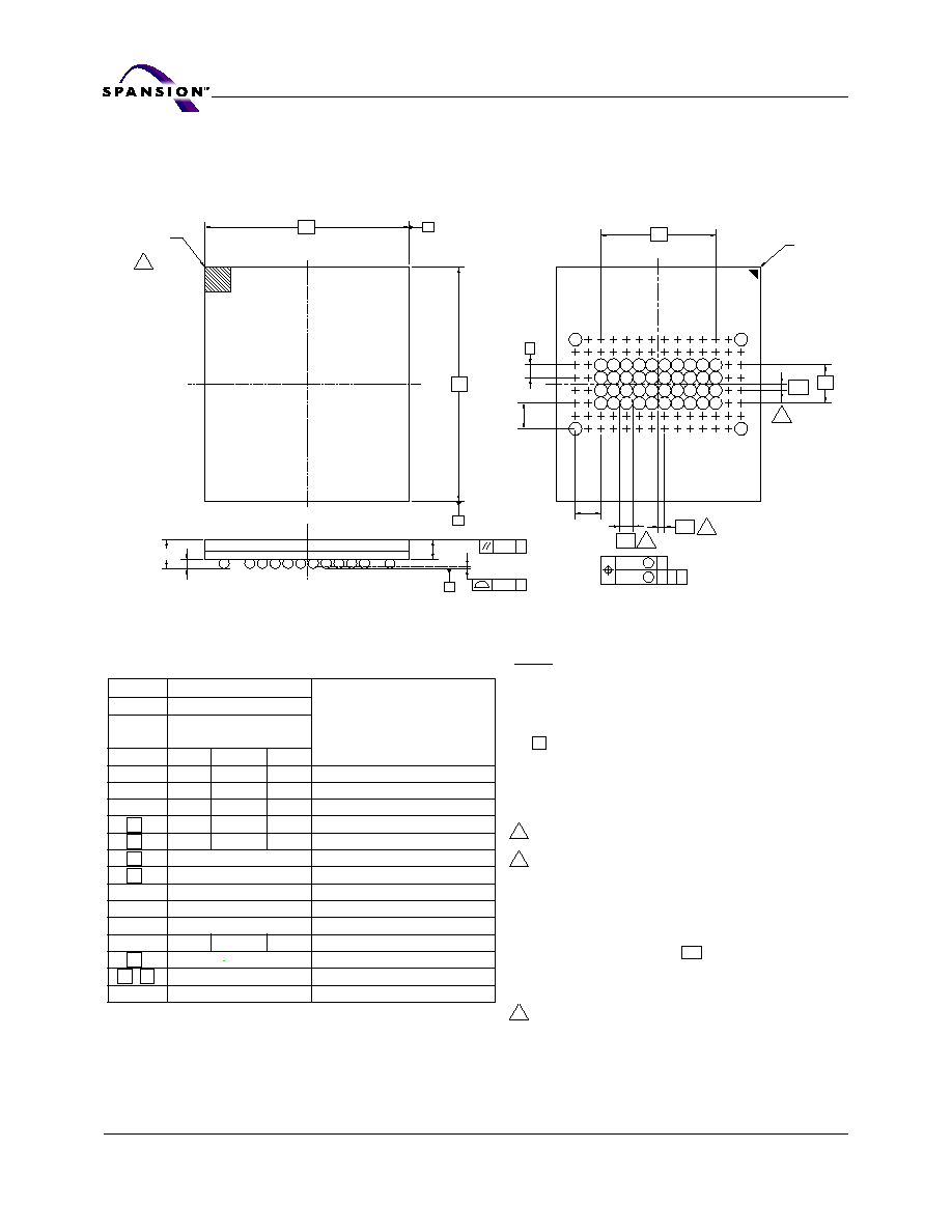
10
S71NS128JA0/S71NS064JA0
31136A1 February 5, 2004
P r e l i m i n a r y
PHYSICAL DIMENSIONSS71NS064JA0
NLB044
--
44
-Ball Very Thin Fine-Pitch Ball Grid Array (FBGA)
9.2 x 8
mm Package
* For reference only. BSC is an ANSI standard for Basic Space Centering
PACKAGE
NLB 044
JEDEC
N/A
8.00 mm x 9.20 mm NOM
NOTE
PACKAGE
SYMBOL
MIN
NOM
MAX
A
1.05
---
1.20
OVERALL THICKNESS
A1
0.20
---
---
BALL HEIGHT
A2
0.85
0.91
0.97
BODY THICKNESS
D
7.90
8.00
8.10
BODY SIZE
E
9.10
9.20
9.30
BODY SIZE
D1
4.50 BSC.
BALL FOOTPRINT
E1
1.50 BSC.
BALL FOOTPRINT
MD
10
ROW MATRIX SIZE D DIRECTION
ME
4
ROW MATRIX SIZE E DIRECTION
N
44
TOTAL BALL COUNT
b
0.25
0.30
0.35
BALL DIAMETER
e
0.50 BSC.
BALL PITCH
SD / SE
0.25 BSC.
SOLDER BALL PLACEMENT
---
DEPOPULATED SOLDER BALLS
3298 \ 16-038.22a1
NOTES:
1. DIMENSIONING AND TOLERANCING PER ASME Y14.5M-1994.
2. ALL DIMENSIONS ARE IN MILLIMETERS.
3. BALL POSITION DESIGNATION PER JESD 95-1, SPP-010 (EXCEPT
AS NOTED).
4. e REPRESENTS THE SOLDER BALL GRID PITCH.
5. SYMBOL "MD" IS THE BALL ROW MATRIX SIZE IN THE
"D" DIRECTION.
SYMBOL "ME" IS THE BALL COLUMN MATRIX SIZE IN THE
"E" DIRECTION.
N IS THE TOTAL NUMBER OF SOLDER BALLS.
6
DIMENSION "b" IS MEASURED AT THE MAXIMUM BALL
DIAMETER IN A PLANE PARALLEL TO DATUM C.
7
SD AND SE ARE MEASURED WITH RESPECT TO DATUMS
A AND B AND DEFINE THE POSITION OF THE CENTER
SOLDER BALL IN THE OUTER ROW.
WHEN THERE IS AN ODD NUMBER OF SOLDER BALLS IN
THE OUTER ROW PARALLEL TO THE D OR E DIMENSION,
RESPECTIVELY, SD OR SE = 0.000.
WHEN THERE IS AN EVEN NUMBER OF SOLDER BALLS IN
THE OUTER ROW, SD OR SE = e/2
8. NOT USED.
9. "+" INDICATES THE THEORETICAL CENTER OF DEPOPULATED
BALLS.
10 A1 CORNER TO BE IDENTIFIED BY CHAMFER, LASER OR INK
MARK, METALLIZED MARK INDENTATION OR OTHER MEANS.
A1 CORNER
INDEX MARK
D
A
10
E
A1
SEATING PLANE
C
0.10
A2
C
B
A
C
0.08
NF1
NF3
2
1
3
4
5
6
9
8
7
10
A
NF2
C
D
NF4
B
e
1.00
SE
E1
D1
SD
b
1.00
A
M
M
C
C
0.05
0.15
B
A1 CORNER
7
7
6

February 5, 2004 31136A1
S71NS128JA0/S71NS064JA0
11
P r e l i m i n a r y
Device History
Device/Model Number
Revision
Autoselect 0003h Contents
Major Reason(s) for Change
S71NS128JA0BA00
Initial (ES)
EMLSI
712Eh
Initial release
S71NS128JA0BAW01
Initial (ES)
EMLSI
711Eh
Initial release
S71NS0128JA0BFW01
Second (ES)
EMLSI
711Dh
t
CSS
and t
AVDH
Timing Update
S71NS064JA0BAW21
Second (ES)
Micron
711Dh
t
CSS
and t
AVDH
Timing Update
S71NS064JA0BFW21

12
S71NS128JA0/S71NS064JA0
31136A1 February 5, 2004
P r e l i m i n a r y
APPENDIX A: DAISY CHAIN INFORMATION
Table 1. Daisy Chain Part for 128/16Mbit Multi-Chip Products (NLA048, 10 x 11 mm)
Table 2. NLA048 Package Information
Table 3. NLA048 Connections
Daisy Chain Part
Number
Package Marking
Daisy Chain
Connection
Spansion
128/16Mb MCP
Part Number
Flash Description
Lead (Pb) - Free
Compliant:
S99DCNLA048MSA002
Lead (Pb) - Free:
S99DCNLA048MSF002
99DCNLA048MSA00
99DCNLA048MSF00
Substrate
S71NS128JA0
128-Mbit 110nm Flash
16-Mbit pSRAM
Component Type/Name
NLA048
Solder resist opening
0.25 + 0.05 mm
Daisy Chain Connection Level
On Substrate
Lead-Free Compliant
Yes
Quantity per Reel
550 (300 units per reel by special request to factory)
C1D1
C6D6
A10B10
A5B5
C2D2
C7D7
A9B9
A4B4
C3D3
C8D8
A8B8
A3B3
C4D4
C9D9
A7B7
A2B2
C5D5
C10D10
A6B6
A1B1
On substrate
NF1NF4
NF2NF5
NF16-NF19
NF17-NF20

February 5, 2004 31136A1
S71NS128JA0/S71NS064JA0
13
P r e l i m i n a r y
Figure 1. NLA048 Daisy Chain Layout
(Top View, Balls Facing Down)
1
2
3
4
5
6
7
8
9
10
A
B
C
D
NF16
NF17
NF4
NF5
NF2
NF20
NF1
NF19

14
S71NS128JA0/S71NS064JA0
31136A1 February 5, 2004
P r e l i m i n a r y
APPENDIX B: DAISY CHAIN INFORMATION
Table 4. Daisy Chain Part for 64/16Mbit Multi-Chip Products (NLB044, 9.2 x 8 mm)
Table 5. NLB044 Package Information
Table 6. NLB044 Connections
Daisy Chain Part Number
Package Marking
Daisy Chain
Connection
Spansion
64/16Mb MCP
Part Number
Description
Lead (Pb) - Free Compliant:
S99DCNLB044MSA002
Lead (Pb)- Free:
S99DCNLB044MSF002
99DCNLB044MSA00
99DCNLB044MSF00
Substrate
Level
S71NS064JA0
64-Mbit 110nm Flash
16-Mbit pSRAM
Component Type/Name
NLB044
Solder resist opening
0.25 + 0.05 mm
Daisy Chain Connection Level
On Substrate
Lead-Free Compliant
Yes
Quantity per Reel
600 (300 units per reel by special request to factory)
C1D1
C6D6
A10B10
A5B5
C2D2
C7D7
A9B9
A4B4
C3D3
C8D8
A8B8
A3B3
C4D4
C9D9
A7B7
A2B2
C5D5
C10D10
A6B6
A1B1
On substrate
NF1NF3
NF2NF4

February 5, 2004 31136A1
S71NS128JA0/S71NS064JA0
15
P r e l i m i n a r y
Figure 2. NLB044 Daisy Chain Layout
(Top View, Balls Facing Down)
1
2
3
4
5
6
7
8
9
10
A
B
C
D
NF3
NF4
NF1
NF2

16
S71NS128JA0/S71NS064JA0
31136A1 February 5, 2004
P r e l i m i n a r y
pSRAM CHARACTERISTICS
pSRAM Device Bus Operations
Legend: L= Logic0, H= Logic1, X= Don't care
pSRAM DC Characteristics
CS#
OE#
WE#
LB#
UB#
AVD#
A[19-16]
A/DQ[15-0]
Mode
Power
H
X
X
X
X
X
X
HIGH-Z
Deselected
Standby
L
H
H
X
X
H
X
HIGH-Z
Output Disabled
Active
L
X
X
H
H
X
X
HIGH-Z
Output Disabled
Active
L
H
L
H
H
H
X
Data In
Configuration
Register Write
Access
Active
L
L
H
H
H
H
X
Data Out
Configuration
Register Read
Access
Active
L
H
H
H
H
L
Addr In
Addr In
Address Input
Active
L
L
H
L
H
H
X
Data Out
Lower Byte Read
Active
L
L
H
H
L
H
X
Data Out
Upper Byte Read
Active
L
L
H
L
L
H
X
Data Out
Word Read
Active
L
H
L
L
H
H
X
Data In
Lower Byte Write
Active
L
H
L
H
L
H
X
Data In
Upper Byte Write
Active
L
H
L
L
L
H
X
Data In
Word Write
Active
Symbol
Item
Test Conditions
Min
Typ
Max
Unit
I
LI
Input Leakage Current
V
IN
= V
SS
to V
CC
-1
1
µA
I
LO
Output Leakage Current
CS# = V
IH
or OE# = V
IH
or WE# = V
IL
,
V
IO
= V
SS
to V
CC
-1
1
µA
I
CC1
Average Operating Current
Cycle Time = 1 µs, 100% duty, I
IO
= 0 mA,
CS#
0.2 V, V
IN
0.2V or V
IN
V
CC
0.2V
5
mA
I
CC2
Cycle Time = Min, I
IO
= 0 mA, 100% duty,
CS# = V
IL
, V
IN
= V
IH
or V
IL
20
mA
V
OL
Output Low Voltage
I
OL
= 0.1 mA
0.1
V
V
OH
Output High Voltage
I
OH
= -0.1 mA
V
CC
0.1 V
V
I
SB1
Standby Current (CMOS)
CS#
V
CC
0.2V, Other Inputs = 0~V
CC
70
µA

February 5, 2004 31136A1
S71NS128JA0/S71NS064JA0
17
P r e l i m i n a r y
pSRAM CHARACTERISTICS
pSRAM AC Characteristics
Notes:
1. t
WRL
(min) = 85 ns for continuous write operation over 50 times. (Only in case of WE# controlled write operation)
2. t
BW
(min) = 85 ns for continuous write operation over 50 times. (Only in case of UB#, LB# controlled write operation)
Parameter List
Symbol
Min
Max
Units
Common
AVD# Low Pulse
t
AVD
20
ns
Address setup to AVD# rising edge
t
AVDS
20
ns
Address hold from AVD# rising edge
t
AVDH
5
ns
Chip enable setup to AVD# rising edge
t
CSS
10
ns
Read
AVD# low to Data Valid time
t
ACC1
90
ns
Address access time
t
ACC2
90
ns
Chip Enable to data output
t
ACC3
90
ns
Address disabled to output enable
t
ADOE
0
ns
Output enable to valid output
t
OE
50
ns
UB#, LB# enable to data output
t
UBLBA
40
ns
UB#, LB# enable to Low-Z output
t
BLZ
15
ns
Output enable to Low-Z output
t
OLZ
15
ns
Chip disable to High-Z output
t
HZ
20
ns
UB#, LB# disable to High-Z output
t
BHZ
15
ns
Output disable to High-Z output
t
OHZ
15
ns
Write
AVD# low to end of write
t
ACW1
90
ns
Address valid to end of write
t
ACW2
90
ns
Chip enable to end of write
t
ACW3
90
ns
Write pulse low
t
WRL
70
(Note 1)
ns
UB#, LB# valid to end of write
t
BW
70
(Note 2)
ns
Data to write time overlap
t
DW
35
ns
Data hold from write time
t
DH
0
ns

18
S71NS128JA0/S71NS064JA0
31136A1 February 5, 2004
P r e l i m i n a r y
pSRAM CHARACTERISTICS
pSRAM Device Operation
The access is performed in two stages. The first stage is address latching. The
first stage takes place between points A and B in timing diagram. At this stage,
the Chip Select (CS#) to the device is asserted. The random access is enabled
either from the point the address becomes stable, the falling edge of the AVD#
signal or from the falling edge of the last CS# signal.
The second stage is the read or write access. This takes place between points B
and C in timing diagram. In case of read access, the multiplexed address/ data
bus A/DQ[15-0] changes its direction. It is important to notice t
OE
when it is dom-
inant that the device gets into the read cycle since the address is available long
before the device output is enabled.
pSRAM Read Access
The read access (See Figures
5
,
6
) is initiated by applying the address to the mul-
tiplexed address/data bus A/DQ[15-0] and address bus A[19-16]. When the
address is stable, the device chip select (CS#) is set active low. At point A, the
AVD# signal is taken low and the latch becomes transparent. This allows the ad-
dress to be propagated to the memory array. The address is stable at the rising
edge of the AVD# signal. The AVD# signal goes high at point B in which the ad-
dress latch is completed. At this point the read cycle is entered. The OE# signal
is set active low. This changes the direction of the bus. The status of control sig-
nals UB# and LB# is set according to the access. Data is read at point C.
pSRAM Write Access
The write access (Figures
7
and
8
) is initiated by applying the address to the mul-
tiplexed address/data bus A/DQ[15-0] and the address bus A[19-16]. When the
address is stable, the device chip select (CS#) is asserted active low. At point A,
the AVD# signal is taken low and the latch becomes transparent. This allows the
address to be propagated to the memory array. The address is stable at the rising
edge of the AVD# signal. The AVD# signal goes high at point B in which the ad-
dress latch is completed. At this point, the second stage of the write process is
entered. Data is input to the multiplexed address/data bus. The WE# signal is set
low and control signals UB# and LB# are set according to the access.
Configuration Register Access
A configuration register is needed to control the different modes of the RAM. The
configuration register consists of 16 bits and it can be accessed when LB# and
UB# signals are de-asserted. The AVD# signal is not used during configuration
access. Configuration registers read access is shown in Figure 3 and write ac-
cesses in Figure 4.
The configuration registers bits are specified in Table
7
. Writing to bits 15 - 8,
does not change the device operation in normal mode.

February 5, 2004 31136A1
S71NS128JA0/S71NS064JA0
19
P r e l i m i n a r y
Table 7. Configuration Register
Figure 3. Configuration Register Read Access
Figure 4. Configuration Register Write Access
Bit Number
Definition
Remark
15 - 8
Don't use in normal mode
7 - 4
Reserved for future use
3 - 2
Reduced memory size
00 = Full array
01 = 1/2 array
10 = 1/4 array
11 = 1/8 array
1 - 0
Temperature
00 = Internal temperature sensing
A/DQ15-0
CS#
OE#
LB#, UB#, WE#
High
Don't Care
Data Valid
t
ACC3
t
OE
A/DQ15-0
CS#
WE#
LB#, UB#, OE#
Data Valid
ACC3
WRL
t
t

20
S71NS128JA0/S71NS064JA0
31136A1 February 5, 2004
P r e l i m i n a r y
pSRAM CHARACTERISTICS
pSRAM Read Access Timing Diagrams
Figure 5. pSRAM Read Cycle 1 (WE# = V
IH
)
Figure 6. pSRAM Read Cycle 2 (WE# = V
IH
)
Notes:
1. To have t
OE
= t
UBLBA
= 50 ns, time for the AVD# rising edge to OE# low and that for AVD# rising edge to UB#/LB# low must
be over 30 ns at least.
2. If invalid address signals shorter than min. t
ACC
are continuously repeated for over 4
µ
s, the device needs a normal read
timing (t
ACC
) or needs to sustain standby state for min. t
ACC
at least once in every 4
µ
s.
t
ADOE
t
AVDS
CS#
Address/Data
UB#, LB#
OE#
t
ACC1
t
AVD
Address Valid
Data Valid
t
CSS
t
UBLBA
AVD#
A
B
t
BHZ
t
HZ
t
OHZ
t
OLZ
t
BLZ
t
AVDH
C
t
OE
t
ACC3
t
ADOE
t
AVDS
CS#
Address/Data
UB#, LB#
OE#
t
AVD
Address Valid
Data Valid
t
CSS
t
UBLBA
AVD#
A
B
t
BHZ
t
HZ
t
OHZ
t
OLZ
t
BLZ
t
AVDH
C
t
ACC2
t
OE

February 5, 2004 31136A1
S71NS128JA0/S71NS064JA0
21
P r e l i m i n a r y
pSRAM CHARACTERISTICS
pSRAM Write Access Timing Diagrams
Figure 7. pSRAM Write Cycle 1 (OE# = V
IH
)
Figure 8. pSRAM Write Cycle 2 (OE# = V
IH
)
Notes:
1. A write occurs during the overlap (t
WRL
) of low CS#, low WE# and low UB# or LB#. A write begins at the last transition among
low CS# and low WE# with asserting UB# or LB# low for single byte operation or simultaneously asserting UB# and LB# low
for word operation. A write ends at the earliest transition among high CS# and high WE#. The t
WRL
is measured from the
beginning of write to the end of write.
t
AVDH
t
AVDS
CS#
Address/Data
UB#, LB#
WE#
t
ACW3
t
ACW1
t
AVD
t
CSS
t
BW
AVD#
A
B
C
t
DW
t
DH
Data Valid
Address Valid
t
WRL
t
AVDH
t
AVDS
CS#
Address/Data
UB#, LB#
WE#
t
AVD
t
CSS
t
BW
AVD#
A
B
C
t
DW
t
DH
Data Valid
Address Valid
t
WRL
t
ACW2

22
S71NS128JA0/S71NS064JA0
31136A1 February 5, 2004
P r e l i m i n a r y
Revision Summary
Revision A (December 8, 2003)
Initial Release.
Revision A+1 (February 5, 2004)
Global
Converted datasheet to Preliminary to Advanced.
Product Selector Guide
Added additional MCP Model Numbers.
Ordering Information
Updated Ordering options to reflect new Model Numbers.
Added new Valid Combinations and Package Markings to table.
Device History
Updated to reflect addition of Model Numbers.
pSRAM Device Bus Operations
Added two rows for Configuration Register Read/Write Access Mode.
Trademarks and Notice
Copyright © 2004 FASL LLC. All rights reserved.
Spansion, the Spansion logo, MirrorBit, and combinations thereof are registered trademarks of FASL LLC.
ExpressFlash is a trademark of FASL LLC.
Product names used in this publication are for identification purposes only and may be trademarks of their respective companies.