August 2004
ASM4SSTVF16857
rev 2.0
Alliance Semiconductor
2575, Augustine Drive
Santa Clara, CA
Tel: 408.855.4900
Fax: 408.855.4999
www.alsc.com
Notice: The information in this document is subject to change without notice.
DDR 14-Bit Registered Buffer
Features
·
Fully JEDEC JC40 - JC42.5 compliant for DDR1
applications to include: PC1600, PC2100, PC2700
& PC3200 ( > JEDEC defined DDR 400 @
200MHz )
·
Low voltage operation; VDD: 2.3V - 2.7V.
·
SSTL_2 Class II outputs.
·
Differential clock inputs.
·
Available in 48 pin TSSOP and TVSOP packages.
Product Description
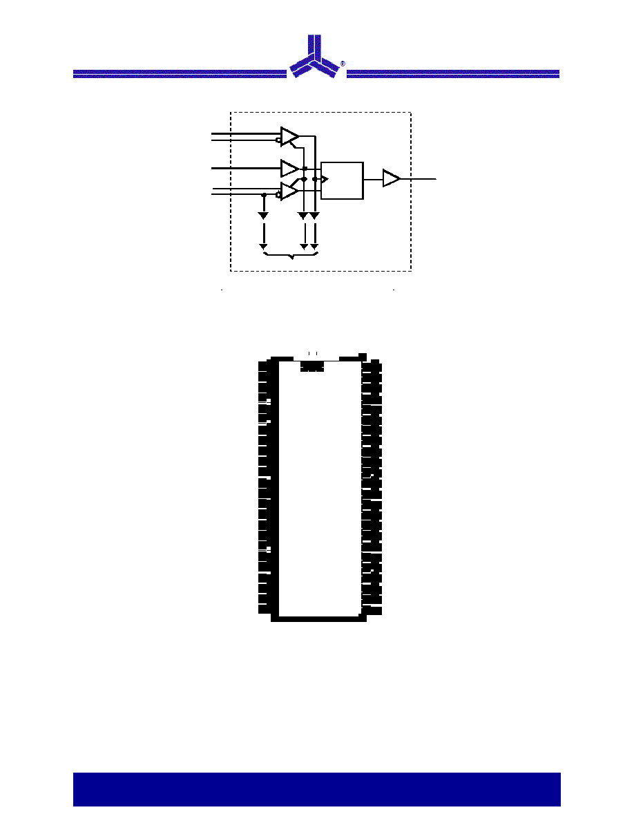
The ASM4SSTVF16857 is a universal 14-bit register
(D F/F based), designed for 2.3V to 2.7V V
DD
. The
device supports SSTL_2 I/O levels, and is fully
compliant with the JEDEC JC40, JC42.5 DDR I
specifications covering PC1600, PC2100, PC2700, and
PC3200 operational ranges. 14-bit refers to 2Q outputs
for each D input - designed for use in Stacked Registers
(stacked memory devices), Buffered DIMM applications.
Data flow from D to Q is controlled by the differential
clock (CLK/CLKB) along with a controlled reset
(RESETB). The positive edge of CLK is used to trigger
the data transfer, and CLKB is used to maintain
sufficient noise margins, whereas the RESETB input is
designed and intended for use at power-up.
The ASM4SSTVF16857 supports a low power standby
mode of operation. A logic low level at RESETB,
assures that all internal registers and outputs (Q) are
reset to a logic low state, and that all input receivers,
data (D) buffers, and clock (CLK/CLKB) are switched
off. Note that RESETB should be supported with a
LVCMOS level at a valid logic state since VREF may
not be stable during power-up.
To ensure that outputs are at a defined logic state
before a stable clock has been supplied, RESETB must
be held at a logic low level during power-up.
In the JEDEC defined Registered DDR DIMM
application, RESETB is specified to be asynchronous
with respect to
CLK/CLKB; therefore, no timing
relationship can be guaranteed between the two
signals. When entering a low-power standby mode, the
register will be cleared and the outputs will be driven to
a logic low level quickly relative to the time to disable
the differential input receivers. This ensures there are
no "glitches" on any output. However, when coming out
of low power standby mode, the register will become
active quickly relative to the time taken to enable the
differential input receivers. When the data inputs are at
a logic level low and the clock is stable during the low-
to-high transition of RESETB until the input receivers
are fully enabled, the design ensures that the outputs
will remain at a logic low level.
Applications
·
JEDEC and Non JEDEC DDR Memory Modules
·Planar configurations
·Supports PC1600 - PC2100 - PC2700 - PC3200
·
SSTL_2I/O
·
Provides a complete support solution for JEDEC
JC42.5 (JC45) DDR I RDIMMs' when used with the
ASM5CVF857 Zero Delay Buffer.
August 2004
ASM4SSTVF16857
rev 2.0
DDR 14-Bit Registered Buffer
3 of 16
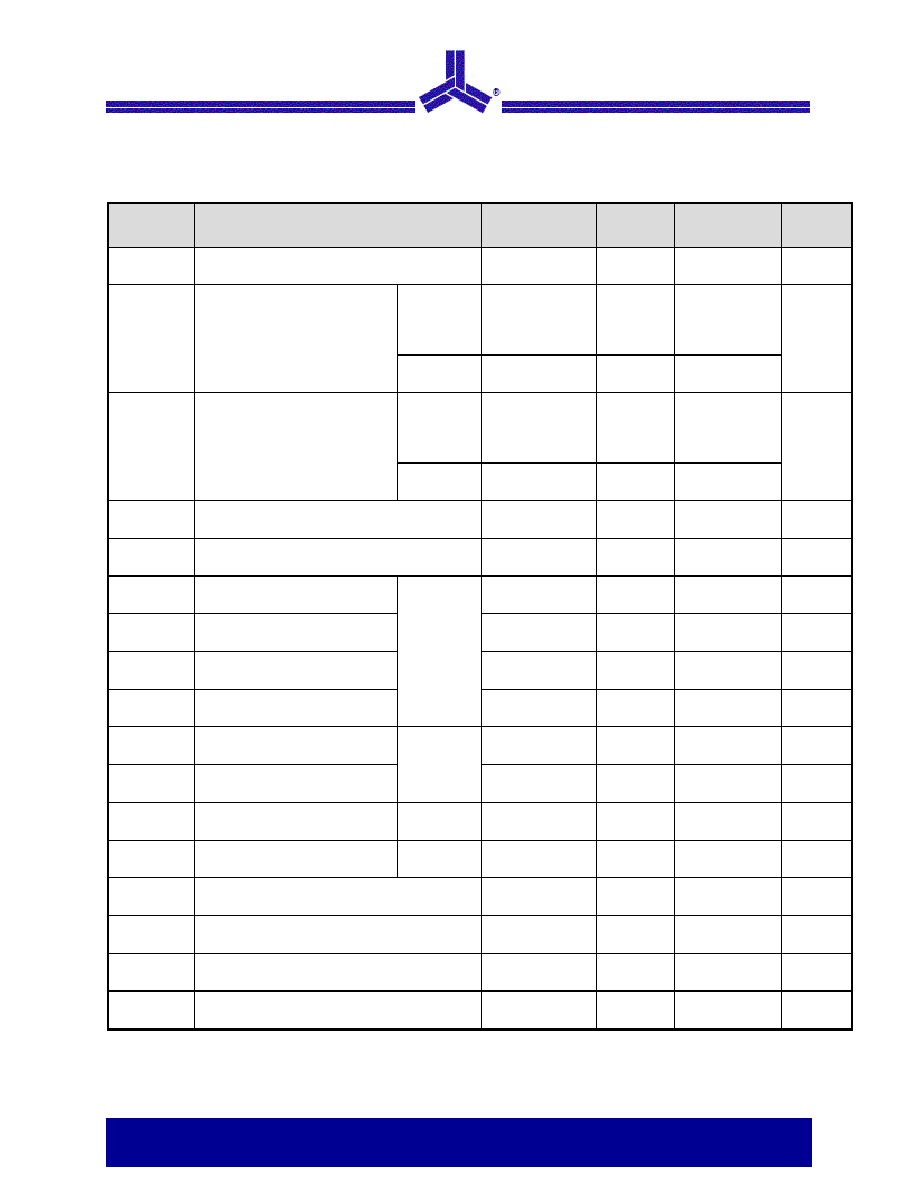
Pin Descriptions
Pin #
Pin Name
Type
Description
1, 2, 5, 6, 7, 10, 11, 14, 15, 18, 19, 20, 23, 24
Q (14:1)
O
Data output.
3, 8, 13, 17, 22, 27, 36, 46
GND
P
Ground to entire chip.
4, 9, 12, 16, 21
VDDQ
P
Output supply voltage.
25, 26, 29, 30, 31, 32, 33, 40, 41, 42, 43, 44, 47, 48
D(14:1)
I
Data input.
38
CLK
I
Positive clock input.
39
CLKB
I
Negative clock input.
28, 37, 45
VDD
P
Core supply voltage.
34
RESETB
I
Rest Active low.
35
VREF
I
Input reference voltage.
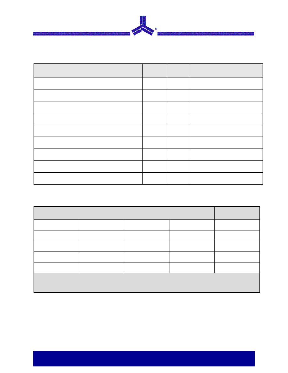
Truth Table
1
Inputs
Q Outputs
RESETB
CLK
CLKB
D
Q
L
X or floating
X or floating
X or floating
L
H
H
H
H
L
L
H
L or H
L or H
X
Q
0
2
Note:
1. H=High signal level, L=Low signal level, = transition from low to high, = transition from high to low, X = don't care
2. Output level before the indicated steady state input conditions were established.