
Alpha Industries, Inc. [978] 241-7000
· Fax [978] 241-7906 · Email sales@alphaind.com · www.alphaind.com
1
Specifications subject to change without notice. 1/02A
LGA Packaged Phase Shifter
for DCS Base Stations
Features
Designed for DCS 1837.5 ± 32.5 MHz Band
100 Degree Phase Shift Range
1.5 Degree Phase Deviation
0.3 dB Insertion Loss Deviation
012 V Control Voltage Range
Specified 33 dBm IP3
Small Footprint LGA Package
PS184-315
Description
The PS184-315 is a voltage controlled phase shifter
specifically designed for use in power amplifier distortion
compensation circuits centered at 1837.5 MHz in DCS
band base stations. Its characteristics are specified in a
70 MHz bandwidth. The PS184-315 employs a monolithic
quadrature hybrid and a pair of selected silicon varactor
diodes to achieve 100 degree phase shift and low insertion
loss. The PS184-315 is packaged in the small outline LGA
(Land Grid Array) surface mount package with the internal
elements affixed to an organic BT substrate.
Preliminary
Parameter
Condition
Min.
Typ.
Max.
Unit
Frequency Range (BW)
F
O =
1837.5
1805
1870
MHz
Phase Shift
At F
O
, C
V
= 12 V
100
Deg.
Phase Deviation in BW
C
V
= 012 V
1.5
2.0
Deg.
Control Voltage (C
V
) Range
0
12
V
Control Current
C
V
= 12 V
1
µA
Insertion Loss in BW
C
V
= 0 V
2.3
dB
I.L. Deviation in BW
C
V
= 012 V
0.3
dB
I.L. Variation At
F
O
, C
V
= 012 V
0.75
dB
VSWR in BW
1.8
IM3
P
IN
= 8 dBm, 1900/1905 MHz, C
V
= 0 V
-50
dBc
IP3
Derived from IM3
33
dBm
Electrical Specifications at 25°C

2
Alpha Industries, Inc. [978] 241-7000
· Fax [978] 241-7906 · Email sales@alphaind.com · www.alphaind.com
Specifications subject to change without notice. 1/02A
LGA Packaged Phase Shifter for DCS Base Stations
PS184-315
Insertion Loss vs.
Frequency and Control Voltage
Frequency (GHz)
Loss (dB)
-2.0
-1.9
-1.8
-1.7
-1.6
-1.5
-1.4
-1.3
-1.2
-1.1
-1.0
1.805
1.820
1.835
1.850
1.865
1.880
0 V
4 V
8 V
12 V
Input/Output Return Loss vs.
Frequency and Control Voltage
Frequency (GHz)
Return Loss (dB)
1.805
1.820
1.835
1.850
1.865
1.880
-60
-50
-40
-30
-20
-10
0
0 V
4 V
8 V
12 V
Insertion Loss Flatness vs. Control Voltage
0
4
2
6
8
10
12
Flatness (dB)
Control Voltage (V)
-0.5
-0.4
-0.3
-0.2
-0.1
0
0.1
0.2
0.3
0.4
0.5
Phase vs. Frequency and Control Voltage
Frequency (GHz)
Phase (Degrees)
1.805
1.820
1.835
1.850
1.865
1.880
0
20
40
60
80
100
120
0 V
4 V
8 V
12 V
Phase Flatness vs. Control Voltage
0
4
2
6
8
10
12
Flatness (dB)
Control Voltage (V)
-2.5
-2.0
-1.5
-1.0
-0.5
0
0.5
1.0
1.5
2.0
2.5
3rd Order Intermod vs. Control Voltage
RF
1
= 1.900 GHz, RF
2
= 1.905 GHz @ 8 dBm
0
4
2
6
8
10
12
Intermod (dBm)
Control Voltage (V)
30
32
34
36
38
40
42
44
46
48
50
Typical Performance Data
LGA Packaged Phase Shifter for DCS Base Stations
PS184-315
Alpha Industries, Inc. [978] 241-7000
· Fax [978] 241-7906 · Email sales@alphaind.com · www.alphaind.com
3
Specifications subject to change without notice. 1/02A
Characteristic
Value
RF Input Power
20 dBm
Control Voltage
15 V
Operating Temperature
-40 to +85°C
Storage Temperature
-40 to +85°C
Absolute Maximum Ratings
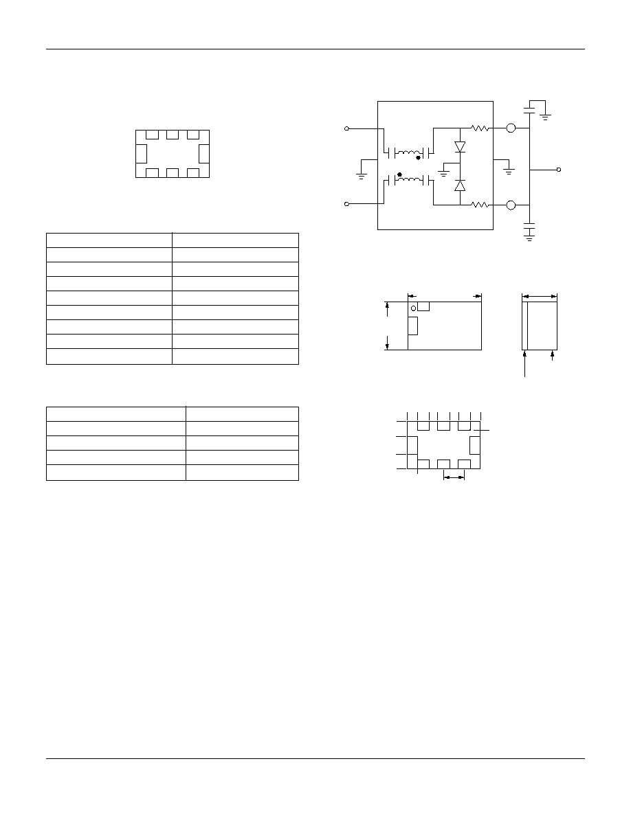
Terminal No.
Terminal Name
A
1
IN/OUT
A
2
GND
A
3
IN/OUT
B
1
GND
B
3
GND
C
1
Vcontrol
C
2
GND
C
3
Vcontrol
-315
B
3
B
1
C
1
C
2
C
3
A
1
A
2
A
3
0.091 (2.32 mm)
0.193 (4.90 mm)
A
1
B
1
0.126
(3.20 mm)
0.079 (2 mm)
ENCAP
0.014 (0.36 mm)
SUBSTRATE
0.000
0.037 (1.00 mm)
0.047 (1.20 mm)
0.079 (2.00 mm)
0.031
(0.775 mm)
0.166 (4.22 mm)
0.135 (3.42 mm)
0.193 (4.90 mm)
0.081 (2.05 mm)
0.058 (1.48 mm)
0.027 (0.68 mm)
0.000
0.112 (2.85 mm)
0.054 (1.370 mm)
0.024 (0.60 mm)
B
3
B
1
C
1
C
2
C
3
A
1
A
2
A
3
IN/OUT
GND
IN/OUT
GND
GND
Vcontrol
Vcontrol
GND
PS184
Pin Out (Bottom View)
Vcontrol
CONTROL
CURRENT
10 pF
10 pF
Vcontrol
RF IN/OUT
RF IN/OUT
Connection Diagram