Alpha Industries, Inc. [781] 935-5150
· Fax [617] 824-4579 · Email sales@alphaind.com · www.alphaind.com
1
Specifications subject to change without notice. 3/01A
GaAs IC 5 Bit Digital Attenuator With
Serial-to-Parallel Driver DC2 GHz
Features
I Positive Voltage Operation (+5 V)
I MLF 5 x 5 mm Leadless Package
I Integrated Silicon Serial-to-Parallel Driver
I Attenuation 0.5 dB Steps to 15.5 dB
MLF 5 x 5 (-310)
AA107-310
Description
The AA107-310 is a GaAs FET IC 5 bit digital attenuator
with a serial-to-parallel driver packaged in a 32 leadless
exposed pad plastic package. It is particularly suited at IF
frequencies where high attenuation accuracy, low insertion
loss and low intermodulation products are required. Typical
applications include base station, wireless and RF data and
wireless local loop gain control circuits.
Parameter
1
Condition
Frequency
2
Min.
Typ.
Max.
Unit
Insertion Loss
3
DC1.0 GHz
1.4
1.7
dB
DC2.0 GHz
1.7
2.2
dB
Attenuation Range
4, 5
15.5
dB
Attenuation Accuracy
4, 5
DC1.0 GHz
± (0.2 + 3% of
Attenuation Setting in dB)
dB
DC2.0 GHz
± (0.4 + 3% of
Attenuation Setting in dB)
dB
VSWR (I/O)
DC2.0 GHz
1.4:1
1.8:1
Switching Characteristics
6
Rise, Fall (10/90% or 90/10% RF)
50
ns
On, Off (50% CTL to 90/10% RF)
100
ns
Video Feedthru
50
mV
Input Power for 1 dB Compression
0.502.0 GHz
+24
+29
dBm
0.05 GHz
+17
+22
dBm
Intermodulation Intercept Point (IP3)
For Two-tone Input Power +5 dBm
0.502.0 GHz
+44
+50
dBm
0.05 GHz
+35
+40
dBm
Control Voltages
V
Low
= 0 to 0.2 V @ 20 µA Max.
V
High
= -5 V @ 300 µA Max.
Electrical Specifications at 25°C (V
CC
= +5 V)
0.001
(0.025 mm)
0.039 (1.00 mm) MAX.
SEATING
PLANE
12° MAX.
0.197 (5.00 mm) BSC
0.197
(5.00 mm)
BSC
1
32
0.187
(4.75 mm) BSC
0.187
(4.75 mm)
BSC
PIN 1
INDICATOR
0.122 (3.10 mm)
± 0.006 (0.15 mm)
0.122 (3.10 mm)
± 0.006 (0.15 mm)
32
1
0.138 (3.50 mm) REF.
0.138
(3.50 mm) REF.
0.019 (0.50 mm) BSC
Preliminary
Parameter
Symbol
Min.
Typ.
Max.
Unit
Input Voltage High
V
IH
(1)
3.5
5.0
V
Input Voltage Low
V
IL
(0)
0
0.5
V
Input Leakage Current
I
L
±0.5
µA
Quiescent Current
I
CC
500
µA
Supply Voltages
V
CC
5.0
V
DC Electrical Characteristics at 25°C (V
CC
= +5 V)
1. All measurements made in a 50
system, unless otherwise specified.
2. DC = 300 kHz.
3. Insertion loss changes by 0.003 dB/°C.
4. Attenuation value referenced above insertion loss.
5. Exposed pad must be connected to RF ground to obtain specified attenuation.
6. Video feedthru measured with 1 ns risetime pulse and 500 MHz bandwidth.

GaAs IC 5 Bit Digital Attenuator With Serial-to-Parallel Driver DC2 GHz
AA107-310
2
Alpha Industries, Inc. [781] 935-5150
· Fax [617] 824-4579 · Email sales@alphaind.com · www.alphaind.com
Specifications subject to change without notice. 3/01A
Truth Table
J
1
J
2
Reset 0.5 dB
1 dB
2 dB
4 dB
8 dB
Attenuation
1
0
0
0
0
0
Insertion Loss
1
1
0
0
0
0
0.5 dB
1
0
1
0
0
0
1 dB
1
0
0
1
0
0
2 dB
1
0
0
0
1
0
4 dB
1
0
0
0
0
1
8 dB
1 1
1
1
1
1
15.5 dB
0
X
X
X
X
X
Insertion Loss
Characteristic
Value
Supply Voltage (V
CC
)
-0.5 to +6 V
Input Voltage (V
I
)
-0.5 V
CC
+ 0.5 V
Power Dissipation (P
D
)
500 mW
Storage Temperature (T
ST
)
-65°C to +125°C
Operating Temperature (T
OP
)
-40°C to +85°C
Absolute Maximum Ratings
Typical Performance Data (V
CC
= +5 V)
-2.0
-1.5
-1.0
-0.5
0
0
0.5
1.0
1.5
2.0
Loss (dB)
Frequency (GHz)
Insertion Loss vs. Frequency
-1.0
-0.8
-0.6
-0.4
0.2
-0.2
0
0
Deviation from Nominal
Attenuation (dB)
Frequency (GHz)
Attenuation Accuracy vs. Frequency
0.5
1.0
1.5
2.0
0.5 dB
1 dB
2 dB
4 dB
8 dB
15.5 dB
0
0.5
1.0
1.5
2.0
VSWR
Frequency (GHz)
VSWR vs. Frequency
1.0
1.1
1.2
1.3
1.4
1.5
Ins. Loss
0.5 dB
1 dB
2 dB
4 dB
8 dB
15.5 dB
Serial Data Input
V
IL
(0) = 0 to 0.5 V.
V
IH
(1) = 3.5 to 5 V.
X = Don't Care.
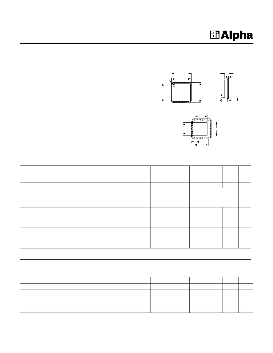
Dimensions in inches (mm).
0.122
(3.10 mm)
SQ.
0.020 (0.50 mm)
0.020
(0.50 mm)
0.020 (0.50 mm)
0.020
(0.50 mm)
0.013 (0.33 mm)
Surface Mount Land Pattern
5 x 5 mm MLF 32 Lead

GaAs IC 5 Bit Digital Attenuator With Serial-to-Parallel Driver DC2 GHz
AA107-310
Alpha Industries, Inc. [781] 935-5150
· Fax [617] 824-4579 · Email sales@alphaind.com · www.alphaind.com
3
Specifications subject to change without notice. 3/01A
J
1
GND
0.025
µ
F
0.01
µ
F
LE
SCK
SDA
GND
GND
GND
GND
GND
GND
GND
GND
GND
Pin 1
Pin 32
GND
GND
GND
GND
GND
J
2
GND
GND
GND
GND
GND
GND
RST
S
OUT
V
CC
C
2
C
1
V
SS
0.01
µ
F
Pin Out
Pin
Symbol
Function
1
S
OUT
Serial Data Output
24
GND
Ground
5
J
1
RF Input/Output
619
GND
Ground
20
J
2
RF Input/Output
2123
GND
Ground
24
RST
Reset
25
LE
Latch Enable
26
SDA
Serial Data Input
27
SCK
Serial Clock Input
28
V
SS
Low Output Voltage Level
29
GND
Ground
30
C
2
Charge Pump Capacitor
31
C
1
Charge Pump Capacitor
32
V
CC
Supply Voltage
Parameter
Symbol
Min.
Typ.
Max.
Unit
LE Setup Time
T
1
15
ns
SDA Setup Time
T
2
15
ns
SDA Hold Time
T
3
10
ns
LE Hold Time
T
4
10
ns
Clock Period
T
5
60
ns
Timing Diagram
LE
SCK
SDA
T
1
T
2
T
3
T
5
T
4