Äîêóìåíòàöèÿ è îïèñàíèÿ www.docs.chipfind.ru
Designed to meet the high-current requirements in industrial and
consumer applications; embedded core, memory, or logic supplies; TVs,
VCRs, and office equipment, the SI-3011ZD voltage regulator offers the
reduced dropout voltage and low quiescent current essential for im-
proved efficiency. This device delivers a regulated output at up to 3 A.
Integrated thermal and overcurrent protection enhance overall system
reliability. Devices with fixed output voltages of 2.5 or 3.3 V are also
available.
Quiescent current does not increase significantly as the dropout
voltage is approached, an ideal feature in standby/resume power systems
where data integrity is crucial. Regulator accuracy and excellent
temperature characteristics are provided by a bandgap reference. An
LS-TTL/CMOS-compatible input gives the designer complete control
over power up, standby, or power down. A pnp pass element provides a
dropout voltage of less than 600 mV at 3 A of load current. Low output
voltages eliminate the need for expensive PWM buck converters. The
low dropout voltage permits more efficient regulation before output
regulation is lost.
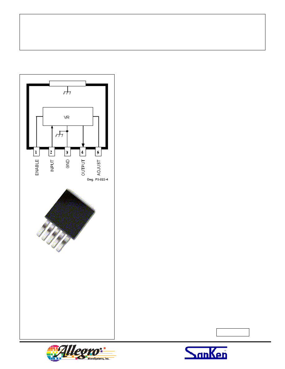
This device is supplied in a 5-lead surface-mount plastic package
(TO-263) with ground tab to provide a low-resistance path for maximum
heat dissipation. A similar device in a flange-mounted (TO-220-style)
high-power package is the SI-3011ZF.
FEATURES
3 A Output Current
Adjustable 1.1~ 5 V Output Voltage
0.6 V Maximum Dropout Voltage at I
O
= 3 A
Fast Transient Response
1 µA Maximum Standby Current
Remote Voltage Sensing
Foldback Current Limiting
Ground Tab for Superior Heat Dissipation
Thermal Protection
APPLICATIONS
TVs, VCRs, Electronic Games
Embedded Core, Memory, or Logic Supplies
Printers and Other Office Equipment
Industrial Machinery
Secondary-Side Stabilization of Multi-Output SMPS
High-Current, Low-Dropout, 1.1~5 V Regulator
Data Sheet
27468.40
Always order by complete part number, e.g., SI-3011ZD-TL ,
where "-TL" indicates tape and reel.
ABSOLUTE MAXIMUM RATINGS
Input Voltage, V
I
. . . . . . . . . . . . . 10 V
Output Current, I
O
. . . . . . . . . . . . . 3 A*
Enable Input Voltage, V
E
. . . . . . . . 6 V
Junction Temperature, T
J
. . . . +125°C
Storage Temperature Range,
T
S
. . . . . . . . . . . . -40°C to +125°C
* Output current rating is limited by input
voltage, duty cycle, and ambient tempera-
ture. Under any set of conditions, do not
exceed a junction temperature of +125°C.
SI-3011ZD
Sanken Power Devices
from Allegro MicroSystems
Linear
Regulators
SI-3011ZD
High-Current,
Low-Dropout,
1.1~5 V Regulator
115 Northeast Cutoff, Box 15036
Worcester, Massachusetts 01615-0036
Linear
Regulators
2
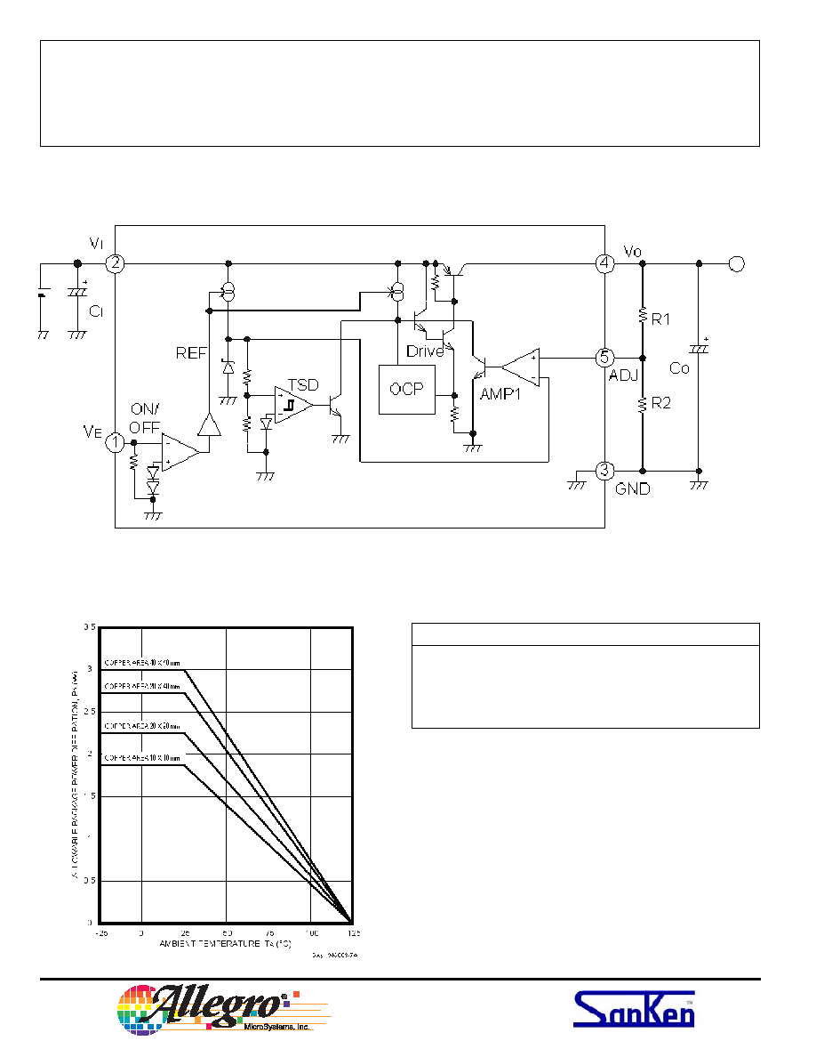
FUNCTIONAL BLOCK DIAGRAM
Copyright © 2004 Allegro MicroSystems, Inc.
Recommended Operating Conditions
Min
Max
Units
DC Input Voltage
--
6
V
DC Output Current
0
3
A
Adjustable Voltage Range
1.2
5
V
Operating Junction Temp.
-20
+100
°C
Allowable Package Power Dissipation
This data sheet is based on Sanken data sheet SSJ-02059E
SI-3011ZD
High-Current,
Low-Dropout,
1.1~5 V Regulator
www.allegromicro.com
Linear
Regulators
3
ELECTRICAL CHARACTERISTICS
at T
A
= +25°C, V
O
= 2.5 V adjusted, V
E
= 2 V (unless otherwise noted).
Limits
Characteristic
Symbol
Test Conditions
Min.
Typ.
Max.
Units
Output Voltage
V
O
V
I
= V
O(nom)
+ 1 V, I
O
= 10 mA
--
V
O(nom)
--
V
V
O(off)
V
E
= 0 V
--
--
0.5
V
Output Volt. Temp. Coeff.
a
VO
0°C
T
J
100°C
--
±0.3
--
mV/°C
Internal Reference Voltage
V
ref
V
I
= V
O(nom)
+ 1 V, I
O
= 10 mA
1.078
1.100 1.122
V
Output Short-Circuit Current
I
OM
V
I
= V
O(nom)
+ 1 V, see note
3.2
--
--
A
Line Regulation
V
O(
VI)
V
I
= 3.0 ~ 5.0 V, I
O
= 10 mA
--
--
10
mV
Load Regulation
V
O(
IO)
V
I
= 3.3 V, I
O
= 0 A ~ 3.0 A
--
--
40
mV
Dropout Voltage
V
Imin
- V
O
I
O
= 3.0 A
--
--
0.6
V
Ground Terminal Current
I
GND
V
I
= V
O(nom)
+ 1 V, I
O
= 0 mA, V
E
= 2.0 V
--
1.0
1.5
mA
V
I
= V
O(nom)
+ 1 V, V
E
= 0 V
--
--
1.0
µA
Enable Input Voltage
V
EH
Output ON
2.0
--
--
V
V
EL
Output OFF
--
--
0.8
V
Enable Input Current
I
EH
V
E
= 2.7 V
--
--
100
µA
I
EL
V
E
= 0 V
--
0
-5.0
µA
Ripple Rejection Ratio
PSRR
V
I
= V
O(nom)
+ 1 V, 100 Hz
f
120 Hz
--
60
--
dB
Thermal Shutdown
T
J
135
152
--
°C
Typical values are given for circuit design information only.
Note: Output short-circuit current is at point where output voltage has decreased 5% below V
O(nom)
.
SI-3011ZD
High-Current,
Low-Dropout,
1.1~5 V Regulator
115 Northeast Cutoff, Box 15036
Worcester, Massachusetts 01615-0036
Linear
Regulators
4
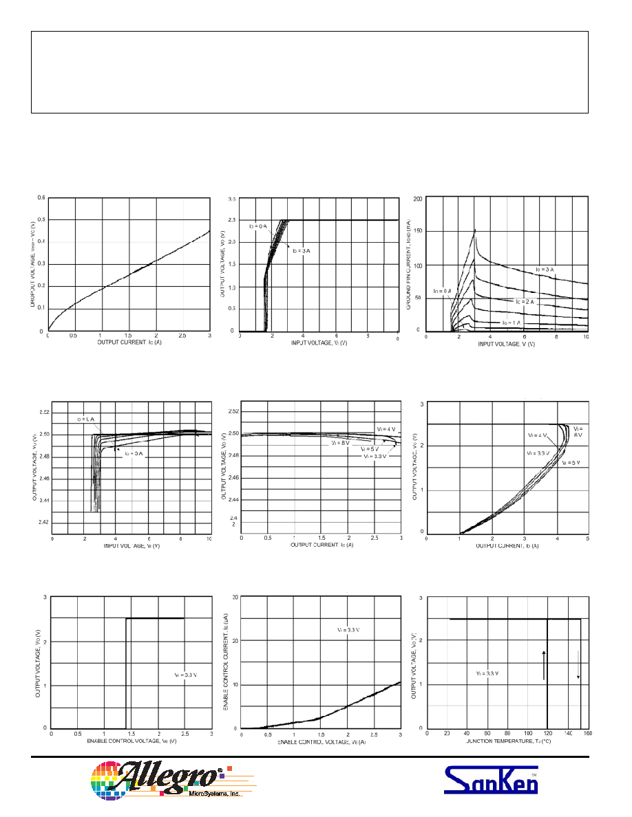
TYPICAL CHARACTERISTICS
(V
O
= 2.5 V adjusted, T
A
= 25°C)
Dropout Voltage
Low-Voltage Behavior
GND Pin Current
Line Regulation
Load Regulation
ENABLE Control Voltage
Overcurrent Protection
ENABLE Control Current
Thermal Protection
SI-3011ZD
High-Current,
Low-Dropout,
1.1~5 V Regulator
www.allegromicro.com
Linear
Regulators
5
APPLICATIONS INFORMATION
Input Capacitor
(C
I
, 0.1 µF to 10 µF). This is necessary
either when the input line includes inductance or when the
wiring is long.
Output Capacitor
(C
O
, > 47 µF). This device is not
designed for a use with a very low ESR output capacitor
such as a ceramic capacitor. Output oscillation may occur
with that kind of capacitor.
Output Voltage Adjustable Resistors
(R1 and R2).
The output voltage is adjusted by R1 and R2. 10 k
or
11 k
for R2 is recommended.
R1 = (V
O
V
ref
)/(V
ref
/R2)
For an output voltage of 1.8 V or less, add a 10 k
resistor
between ADJ and the junction of R1 and R2.
Determination of DC Input Voltage.
The minimum
input voltage V
I
(min) should be higher than the sum of the
fixed output voltage and the maximum rated dropout
voltage. If setting the output voltage lower than 2.0 V, the
minimum input voltage should be more than 2.4 V.
Overcurrent Protection.
The SI-3000ZD series has a
built-in fold-back type overcurrent protection circuit, which
limits the output current at a start-up mode. It thus cannot
be used in applications that require current at the start-up
mode such as:
(1) constant-current load,
(2) power supply with positive and negative outputs to
common load (a center-tap type power supply), or
(3) raising the output voltage by putting a diode or a
resistor between the device ground and system ground.
Thermal Protection.
Circuitry turns off the pass
transistor when the junction temperature rises above 135°C.
It is intended only to protect the device from failures due to
excessive junction temperatures and should not imply that
output short circuits or continuous overloads are permitted.
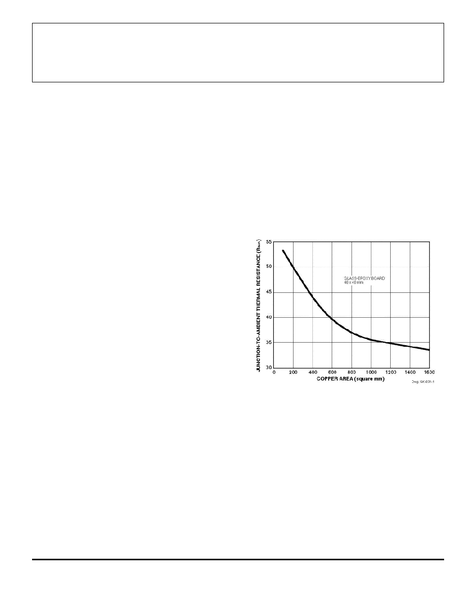
Heat Radiation and Reliability.
The reliability of the
IC is directly related to the junction temperature (T
J
) in its
operation. Accordingly, careful consideration should be
given to heat dissipation.
The inner frame on which the integrated circuit is mounted
is connected to the GND terminal (pin 3). Therefore, it is
very effective for heat radiation to enlarge the copper area
that is connected to the GND terminal. The graph illus-
trates the effect of the copper area on the junction-to-
ambient thermal resistance (R
JA
).
The junction temperature (T
J
) can be determined from
either of the following equations:
T
J
= (P
D
× R
JA
) + T
A
or
T
J
= (P
D
× R
JT
) + T
T
where P
D
= I
O
× (V
I
V
O
) and
R
JT
= 3°C/W.
Parallel Operation.
Parallel operation to increase load
current is not permitted.