
Datasheet
26180.1
10
A6800/A6801
DABiC-5 Latched Sink Drivers
The A6800 and A6801 latched-input BiMOS ICs merge high-current,
high-voltage outputs with CMOS logic. The CMOS input section con-
sists of 4 or 8 data (`D' type) latches with associated common CLEAR,
STROBE, and OUTPUT ENABLE circuitry. The power outputs are
bipolar NPN Darlingtons. This merged technology provides versatile,
fl exible interface. These BiMOS power interface ICs greatly benefi t the
simplifi cation of computer or microprocessor I/O. The A6800 ICs each
contain four latched drivers. A6801 ICs contain eight latched drivers.
The CMOS inputs are compatible with standard CMOS circuits. TTL
circuits may mandate the addition of input pull-up resistors. The bipolar
Darlington outputs are suitable for directly driving many peripheral/
power loads: relays, lamps, solenoids, small dc motors, etc.
All devices have open-collector outputs and integral diodes for induc-
tive load transient suppression. The output transistors are capable of
sinking 600 mA and will withstand at least 50 V in the OFF state.
Because of limitations on package power dissipation, the simultaneous
operation of all drivers at maximum rated current can only be accom-
plished by a reduction in duty cycle. Outputs may be paralleled for
higher load current capability.
The A6800SA is furnished in a standard 14-pin DIP; the A6800SL and
A6801SLW in surface-mountable SOICs; the A6801SA in a 22-pin
DIP with 0.400" (10.16 mm) row centers; the A6801SEP in a 28-lead
PLCC. These devices are lead (Pb) free, with 100% matte tin plated
leadframes.
3.3 V to 5 V logic supply range
To 10 MHz data input rate
High-voltage, high-current outputs
Darlington current-sink outputs, with
improved low-saturation voltages
Use the following complete part numbers when ordering:
AB SO LUTE MAX I MUM RAT INGS
Part Number
Pins
Package
A6800SA-T
14
DIP
A6800SL-T
14
SOIC
A6801SA-T
22
DIP
A6801SEP-T
28
PLCC
A6801SLW-T
24
SOIC
Output Voltage, V
CE
............................................50 V
Supply Voltage, V
DD
.............................................7 V
Input Voltage Range, V
IN
..............0.3 V to V
DD
+0.3 V
Continuous Collector Current, I
C
........................ 600 mA
Package Power Dissipation, P
D
, see Allowable Power
Disspation chart, page 5
Operating Temperature Range
Ambient Temperature, T
A
............20°C to +85°C
Storage Temperature, T
S
..........55°C to +150°C
Caution: CMOS devices have input-static protection,
but are susceptible to damage when exposed to
extremely high static-electrical charges.
FEATURES
Relays
Lamps
APPLICATIONS
A6800SA
A6801SEP
A6801SLW
A6801SA
A6800SL
CMOS, TTL compatible inputs
Output transient protection
Internal pull-down resistors
Low-power CMOS latches
Solenoids
Small dc motors

2
Worcester, Massachusetts 01615-0036 (508) 853-5000
115 Northeast Cutoff, Box 15036
www.allegromicro.com
A6800/A6801
DABiC-5 Latched Sink Drivers
Datasheet
26180.1
10
Functional Block Diagram
C OMMON
G R OUND
S T R OB E
OUT P UT E NAB LE
IN
N
C OMMON MOS C ONT R OL
T Y P IC AL MOS LAT C H
T Y P IC AL B IP OLAR DR IV E
OUT
N
C LE AR
S UP P LY
V
DD
Typical Input Circuit
IN
V
DD
Allowable Power Dissipation
50
75
100
125
150
2.5
0.5
0
PA
C
K
A
G
E
P
O
W
E
R
D
I
S
S
I
PA
T
I
O
N
(
W
)
A MB IE NT T E MP E R A T UR E (ş C )
2.0
1.5
1.0
25
22-P IN DIP , R
JA
= 56
°C /W
28-LE AD P LC C , R
JA
= 68
°C /W
14-P IN DIP , R
JA
= 73
°C /W
14-LE AD S OIC , R
JA
= 120
°C /W
24-LE AD S OIC , R
JA
= 85
°C /W

3
Worcester, Massachusetts 01615-0036 (508) 853-5000
115 Northeast Cutoff, Box 15036
www.allegromicro.com
A6800/A6801
DABiC-5 Latched Sink Drivers
Datasheet
26180.1
10
ELECTRICAL CHARACTERISTICS
1
Unless otherwise noted: T
A
= 25°C, logic supply operating voltage V
dd
= 3.0 V to 5.5 V
Characteristic
Symbol
Test Conditions
V
dd
= 3.3 V
V
dd
= 5 V
Units
Min.
Typ. Max. Min.
Typ.
Max.
Output Leakage Current
I
CEX
V
OUT
= 50 V
10
10
µA
Output Sustaining Voltage
V
CE(SUS)
I
OUT
= 350 mA, L = 3 mH
35
35
V
Collector-Emitter Saturation
Voltage
V
CE(SAT)
I
OUT
= 100 mA
0.8
1.0
0.8
1.0
V
I
OUT
= 200 mA
0.9
1.1
0.9
1.1
V
I
OUT
= 350 mA (See note 2)
1.0
1.3
1.0
1.3
V
Input Voltage
V
IN(1)
2.2
3.3
V
V
IN(0)
1.1
1.7
V
Input Resistance
R
IN
50
50
k
Logic Supply Current
I
DD(1)
One output on, I
OUT
= 100 mA
1.0
1.0
mA
I
DD(0)
All outputs off
130
150
130
150
µA
Clamp Diode Leakage Current
I
r
V
r
= 50 V
50
50
µA
Clamp Diode Forward Voltage
V
f
I
f
= 350 mA
2.0
2.0
V
Output Fall Time
t
f
V
CC
= 50 V, R1 = 500 , C1 30 pF
80
80
ns
Output Rise Time
t
r
V
CC
= 50 V, R1 = 500 , C1 30 pF
100
100
ns
1
Operation of these devices with standard TTL or DTL may require the use of appropriate pull-up resistors to ensure a minimum logic 1.
2
Because of limitations on package power dissipation, the simultaneous operation of multiple drivers can only be accomplished by reduction in duty cycle.
OUT
N
IN
N
S TR OB E
C L E AR
E NAB L E
t-1
t
0
1
0
0
X
OF F
1
1
0
0
X
ON
X
X
1
X
X
OF F
X
X
X
1
X
OF F
X
0
0
0
ON
ON
X
0
0
0
OF F
OF F
X = irrelevant
t-1 = previous output state
t = present output state
OUTP UT
Truth Table

4
Worcester, Massachusetts 01615-0036 (508) 853-5000
115 Northeast Cutoff, Box 15036
www.allegromicro.com
A6800/A6801
DABiC-5 Latched Sink Drivers
Datasheet
26180.1
10
Timing Requirements and Specifi cations
(Logic Levels are V
DD
and Ground)
NOTE: Information present at an input is transferred
to its latch when the STROBE is high. A high CLEAR
input will set all latches to the output off condition
regardless of the data or STROBE input levels. A high
Key
Description
Time (ns)
A
Minimum data active time before Strobe enabled (Data Set-Up Time)
25
B
Minimum data active time after Strobe disabled (Data Hold Time)
25
C
Minimum Strobe pulse width
50
D
Maximum time between Strobe activation and transition from output on to output off*
500
E
Minimum time between Strobe activation and transition from output off to output on*
500
F
Maximum time between Output Enable activation and transition from output on to output off*
500
G
Minimum time between Output Enable activation and transition from output off to output on*
500
H
Minimum Clear pulse width
50
I
Minimum data pulse width
100
CLEAR
STROBE
OUTPUT
ENABLE
INN
OUTN
A
C
B
C
B
G
D
E
H
A
C
B
I
E
G
F
*Conditions for output transition testing are: V
DD
= 50 V, V
CC
= 5 V, R1 = 500 , C1 30 pF.
OUTPUT ENABLE will set all outputs to the off con-
tdition, regardless of any other input conditions. When
the OUTPUT ENABLE is low, the outputs depend on
the state of their respective latches.

5
Worcester, Massachusetts 01615-0036 (508) 853-5000
115 Northeast Cutoff, Box 15036
www.allegromicro.com
A6800/A6801
DABiC-5 Latched Sink Drivers
Datasheet
26180.1
10
2
3
4
5
6
7
8
9
10
11
12
13
14
SUPPLY
GROUND
CLEAR
OUT
1
OUT
2
OUT
3
Dwg. PP-014A
OUT
4
1
14
1
COMMON
OUTPUT
ENABLE
IN
1
STROBE
IN
2
IN
3
IN
4
V
DD
LATCHES
A6800SL
A6800SA
Note: The A6800SL (SOIC) and the A6800SA
(DIP) are electrically identical and share a com-
mon terminal number assignment.
1
2
3
4
5
6
7
8
9
10
11
12
13
14
15
16
17
18
19
20
21
22
23
24
25
26
27
28
GROUND
OUTPUT
ENABLE
STROBE
K
ST
V
DD
OE
Dwg. PP-037
LATCHES
NC
NC
NC
NC
NC
NC
SUPPLY
LAMP DIODE
COMMON
C
CLEAR
OUT
1
IN
8
OUT
8
OUT
2
OUT
3
OUT
4
OUT
5
OUT
6
OUT
7
IN
1
IN
2
IN
3
IN
4
IN
5
IN
6
IN
7
A6801SEP
2
21
22
SUPPLY
CLEAR
1
OUTPUT
ENABLE
STROBE
V
DD
3
4
5
6
7
16
17
18
19
20
OUT
1
OUT
2
OUT
3
OUT
4
IN
1
IN
2
IN
3
IN
4
7
8
9
10
11
12
13
14
15
GROUND
OUT
5
OUT
6
OUT
7
Dwg. PP-015
OUT
8
COMMON
IN
5
IN
6
IN
7
IN
8
LATCHES
A6801SA
2
23
24
SUPPLY
CLEAR
1
OUTPUT
ENABLE
STROBE
V
DD
3
4
5
6
7
21
22
OUT
1
OUT
2
OUT
3
OUT
4
IN
1
IN
2
IN
3
IN
4
7
8
9
10
11
GROUND
OUT
5
OUT
6
OUT
7
Dwg. PP-015-1
OUT
8
COMMON
IN
5
IN
6
IN
7
IN
8
LATCHES
NO
CONNECTION
NO
CONNECTION
NC
NC
12
13
18
19
20
14
15
16
17
A6801SLW

6
Worcester, Massachusetts 01615-0036 (508) 853-5000
115 Northeast Cutoff, Box 15036
www.allegromicro.com
A6800/A6801
DABiC-5 Latched Sink Drivers
Datasheet
26180.1
10
TYPICAL APPLICATION
UNIPOLAR STEPPER-MOTOR DRIVE
Dwg. No. B -1537
1
2
3
4
5
6
7
8
9
10
11
12
13
14
OUT 2
OUT 3
OUT 4
OUT 1
+30 V
IN 1
IN 2
IN 3
IN 4
S T R OB E
C LE AR
OUT P UT E NAB LE (AC T IV E LOW )
LA
T
C
H
E
S
A6800S A
V
DD
V
DD
+30 V
S T R OB E
IN 1
IN 2
IN 3
IN 4
OUT 1
OUT 2
OUT 3
OUT 4
Dwg. G P -060
S T R OB E
IN 1
IN 2
IN 3
IN 4
OUT 1
OUT 2
OUT 3
OUT 4
Dwg. G P -060-1
UNIPOLAR WAVE DRIVE
UNIPOLAR 2-PHASE DRIVE

7
Worcester, Massachusetts 01615-0036 (508) 853-5000
115 Northeast Cutoff, Box 15036
www.allegromicro.com
A6800/A6801
DABiC-5 Latched Sink Drivers
Datasheet
26180.1
10
A6800SA
Dimensions in Inches
(controlling dimensions)
Dimensions in Millimeters
(for reference only)
NOTES: 1. Exact body and lead configuration at vendor's option within limits shown.
2. Lead spacing tolerance is non-cumulative.
3. Lead thickness is measured at seating plane or below.
0.014
0.008
0.300
BSC
Dwg. MA-001-14A in
0.430
MAX
0.100
BSC
14
1
7
0.280
0.240
0.210
MAX
0.070
0.045
0.015
MIN
0.022
0.014
0.005
MIN
0.150
0.115
8
0.775
0.735
0.355
0.204
7.62
BSC
Dwg. MA-001-14A mm
10.92
MAX
14
1
7
7.11
6.10
5.33
MAX
1.77
1.15
0.39
MIN
0.558
0.356
2.54
BSC
0.13
MIN
3.81
2.93
8
19.68
18.67

8
Worcester, Massachusetts 01615-0036 (508) 853-5000
115 Northeast Cutoff, Box 15036
www.allegromicro.com
A6800/A6801
DABiC-5 Latched Sink Drivers
Datasheet
26180.1
10
A6800SL
NOTES: 1.
Exact body and lead configuration at vendor's option within limits shown.
2.
Lead spacing tolerance is non-cumulative.
0
°
TO 8
°
0.3444
0.3367
0.2440
0.2284
0.050
0.016
Dwg. MA-007-14 in
0.050
BSC
0.0098
0.0075
1
2
3
0.1574
0.1497
0.020
0.013
0.0688
0.0532
0.0040
MIN.
14
8
8.75
8.55
6.20
5.80
1.27
0.40
0
°
TO 8
°
Dwg. MA-007-14A mm
1.27
BSC
0.25
0.19
1
2
3
4.00
3.80
0.51
0.33
1.75
1.35
0.10
MIN.
14
8
Dimensions in Inches
(for reference only)
Dimensions in Millimeters
(controlling dimensions)

9
Worcester, Massachusetts 01615-0036 (508) 853-5000
115 Northeast Cutoff, Box 15036
www.allegromicro.com
A6800/A6801
DABiC-5 Latched Sink Drivers
Datasheet
26180.1
10
Dimensions in Inches
(controlling dimensions)
Dimensions in Millimeters
(for reference only)
NOTES: 1. Exact body and lead configuration at vendor's option within limits shown.
2. Lead spacing tolerance is non-cumulative.
3. Lead thickness is measured at seating plane or below.
22
1
2
3
11
9.65
8.39
5.33
MAX
0.070
0.030
28.44
26.67
0.39
MIN
0.558
0.356
2.54
BSC
0.13
MIN
4.06
2.93
0.381
0.204
10.16
BSC
Dwg. MA-002-22 mm
12.70
MAX
12
22
1
2
3
11
0.380
0.330
0.210
MAX
0.070
0.030
0.015
MIN
0.022
0.014
0.100
BSC
0.005
MIN
0.160
0.115
0.015
0.008
0.400
BSC
Dwg. MA-002-22 in
0.500
MAX
12
1.120
1.050
A6801SA

10
Worcester, Massachusetts 01615-0036 (508) 853-5000
115 Northeast Cutoff, Box 15036
www.allegromicro.com
A6800/A6801
DABiC-5 Latched Sink Drivers
Datasheet
26180.1
10
A6801SEP
Dimensions in Inches
(controlling dimensions)
Dimensions in Millimeters
(for reference only)
NOTES: 1. Exact body and lead configuration at vendor's option within limits shown.
2. Lead spacing tolerance is non-cumulative.
18
12
0.020
MIN
0.050
BSC
1
28
INDEX AREA
Dwg. MA-005-28A in
0.026
0.032
0.013
0.021
26
25
19
11
4
5
0.165
0.180
0.495
0.485
0.456
0.450
0.495
0.485
0.456
0.450
0.219
0.191
0.219
0.191
0.51
MIN
4.57
4.20
1.27
BSC
12.57
12.32
11.582
11.430
1
28
INDEX AREA
Dwg. MA-005-28A mm
0.812
0.661
0.331
0.533
12.57
12.32
26
25
19
18
12
11
4
5
11.58
11.43
5.56
4.85
5.56
4.85
11
Worcester, Massachusetts 01615-0036 (508) 853-5000
115 Northeast Cutoff, Box 15036
www.allegromicro.com
A6800/A6801
DABiC-5 Latched Sink Drivers
Datasheet
26180.1
10
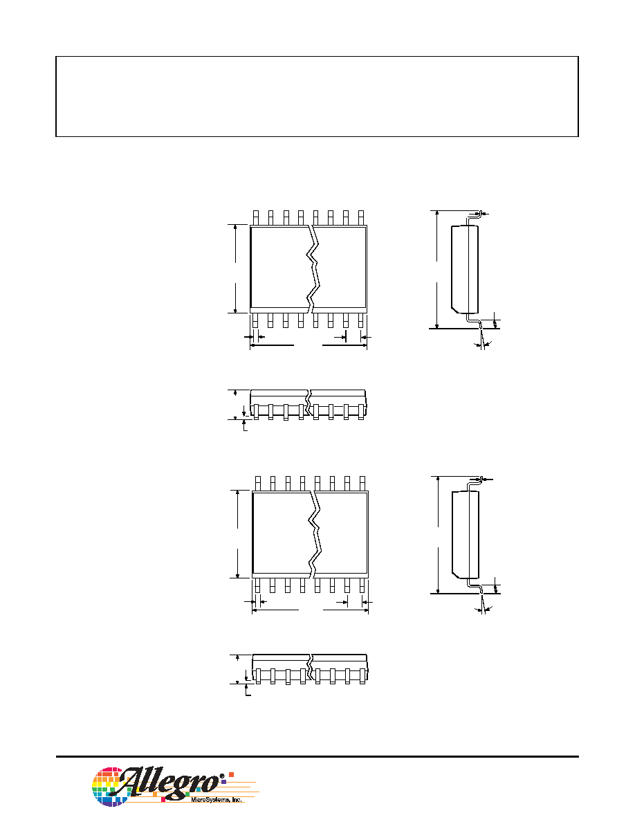
A6801SLW
Dimensions in Inches
(for reference only)
Dimensions in Millimeters
(controlling dimensions)
NOTES: 1.
Exact body and lead configuration at vendor's option within limits shown.
2.
Lead spacing tolerance is non-cumulative.
0
°
TO
8
°
1
2
3
0.020
0.013
0.0040
MIN.
0.0125
0.0091
0.050
0.016
Dwg. MA-008-24A in
0.050
BSC
24
13
0.2992
0.2914
0.419
0.394
0.6141
0.5985
0.0926
0.1043
0
°
TO
8
°
1
24
2
3
0.51
0.33
0.10
MIN.
0.32
0.23
1.27
0.40
Dwg. MA-008-24A mm
1.27
BSC
13
7.60
7.40
10.65
10.00
15.60
15.20
2.65
2.35

12
Worcester, Massachusetts 01615-0036 (508) 853-5000
115 Northeast Cutoff, Box 15036
www.allegromicro.com
A6800/A6801
DABiC-5 Latched Sink Drivers
Datasheet
26180.1
10
The products described here are manufactured under one or
more U.S. patents or U.S. patents pending.
Allegro MicroSystems, Inc. reserves the right to make, from time
to time, such de par tures from the detail spec i fi ca tions as may be
required to permit improvements in the per for mance, reliability,
or manufacturability of its products. Before placing an order, the
user is cautioned to verify that the information being relied upon is
current.
Allegro products are not authorized for use as critical compo-
nents in life-support devices or sys tems without express written
approval.
The in for ma tion in clud ed herein is believed to be ac cu rate and
reliable. How ev er, Allegro MicroSystems, Inc. assumes no re spon -
si bil i ty for its use; nor for any in fringe ment of patents or other
rights of third parties which may result from its use.
Copyright©2003, 2004, 2005 Allegro Microsystems, Inc.