
AME, Inc.
1
AME4624/4625
1-Ohm Low Voltage
SPDT Analog Switch
l
Low R
ON
l
Wide Operation Supply Voltage: 1.8V to 5.5V
l
Fast Switching Time: t
ON
= t
OFF
= 50nS max.
l
TTL-Logic Compatible
l
Pin Compatible with MAX4624/MAX4625
l
Over Thermal Protection
The AME4624/AME4625 analog switches feature low
ON resistance, single-pole, double-throw (SPDT) with
wide operating single power supply voltage range, from
1.8V to 5.5V. The AME4624 offers break-before-make
switching while the AME4625 offers make-before-break
switching.
AME4624/AME4625 has 1
max ON resistance when
+5V power supply is used. These products also have
fast switching speeds, t
ON
= t
OFF
= 50nS max.
AME4624/AME4625 are available in SOT-26 & TSOT-
26 (TSOT-23, 6 pins).
l
Power Routing
l
Battery-Operated Equipment
l
Audio and Video Signal Routing
l
Low-Voltage Data-Acquisition Systems
l
Communications Circuits
l
PCMCIA Cards
l
PC Peripherals
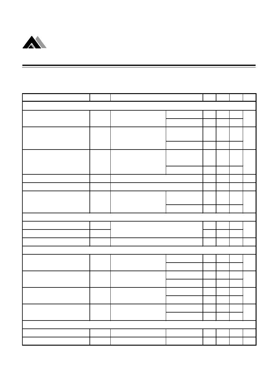
n
General Description
n
Features
n
Applications
n
Functional Block Diagram
In Logic
NC
NO
0
ON
OFF
1
OFF
ON
V
+
IN
NO
COM
NC
GND
l
Guaranteed Break-Before-Make(AME4624)
l
Guaranteed Make-Before-Break(AME4625)

AME, Inc.
2
AME4624/4625
1-Ohm Low Voltage
SPDT Analog Switch
n
Pin Configuration
1
3
2
6
4
5
AME4624
AME4624
1. IN
2. V+
3. GND
4. NC
5. COM
6. NO
n
Pin Description
n
Ordering Information
Note: ww represents the date code and pls refer to Date Code Rule before the page of Package Dimension.
* A line on top of the first letter represents lead free plating such as AZL
Pls consult AME sales office or authorized Rep./Distributor for the availability of package type.
AME4625
1. IN
2. V+
3. GND
4. NC
5. COM
6. NO
1
3
2
6
4
5
AME4625
Part Number
Marking*
Activity Mode
Package
Operating Temp. Range
AME4624AEEY
AZLww
Break-Before-Make
SOT-26
- 40
o
C to + 85
o
C
AME4624AEEYZ
AZLww
Break-Before-Make
SOT-26
- 40
o
C to + 85
o
C
AME4624AEEYL
AZLww
Break-Before-Make
TSOT-26
- 40
o
C to + 85
o
C
AME4624AEEYY
AZLww
Break-Before-Make
TSOT-26
- 40
o
C to + 85
o
C
AME4625AEEY
BAHww
Make-Before-Break
SOT-26
- 40
o
C to + 85
o
C
AME4625AEEYZ
BAHww
Make-Before-Break
SOT-26
- 40
o
C to + 85
o
C
AME4625AEEYL
BAHww
Make-Before-Break
TSOT-26
- 40
o
C to + 85
o
C
AME4625AEEYY
BAHww
Make-Before-Break
TSOT-26
- 40
o
C to + 85
o
C
*Epoxy: Non-Conductive *Epoxy: Non-Conductive
Pin
Pin Name
Pin Description
1
IN
Digital Control Input
2
V+
Positive Supply Voltage Input
3
GND
Ground
4
NC
Analog Switch-Normally Closed
5
COM
Analog Switch-Common
6
NO
Analog Switch-Normally Open

AME, Inc.
3
AME4624/4625
1-Ohm Low Voltage
SPDT Analog Switch
n
Ordering Information
AME4624/4625 x x x
x x
Operating Temperature Range
Number of Pins
Package Type
Pin Configuration
Special Feature
A
1. IN
E: -40
O
C to 85
O
C
E: SOT-2X
Y: 6
L: Low profile
(SOT-26)
2. V+
Z: Lead free
3. GND
Y: Lead free & Low profile
4. NC
5. COM
6. NO
Pin
Configuration
Special Feature
Operating
Temperature Range
Package Type
Number of
Pins

AME, Inc.
4
AME4624/4625
1-Ohm Low Voltage
SPDT Analog Switch
n
Absolute Maximum Ratings
n
Recommended Operating Conditions
Note1: Signals on COM, NC and NO can not exceed V
+
Caution: Stress above the listed absolute maximum rating may cause permanent damage to the device
n
Thermal Information
Parameter
Rating
Unit
V
+
1.8 to 5.5
V
IN
CMOS, TTL Logic
V
Ambient Temperature Range
- 40 to + 85
o
C
Junction Temperature Range
- 40 to + 125
o
C
Parameter
Maximum
Unit
V
+
, IN
6
V
COM , NC , NO
Note 1
V
Continuous Current
COM , NC , NO
300
mA
ESD Classification
B
Parameter
Package Die Attached
Symbol
Maximum
Unit
Thermal Resistance *
(Junction to Case)
JC
140
Thermal Resistance
(Junction to Ambient)
JA
280
Interal Power Dissipation
P
D
400
mW
300
o
C
o
C / W
Maximum Lead Temperature ( 10sec )
SOT-26
Non-Conductive
* Measure
JC
on center of molding compound if IC has no tab.
AME, Inc.
5
AME4624/4625
1-Ohm Low Voltage
SPDT Analog Switch
Parameter
Symbol
Min
Typ Max Units
V
+
= 4.5V
T
A
= +25
O
C
1.0
I
COM
= 100mA
T
A
= T
MIN
to T
MAX
1.2
V
+
= 4.5V
ICOM = 100mA
VNO or VNC = 3.5V
T
A
= T
MIN
to T
MAX
0.15
V
+
= 4.5V
I
COM
= 100mA
V
NO
or V
NC
= 0V, 1V , 2V T
A
= T
MIN
to T
MAX
0.2
NC or NO Off-Capaitance
C
OFF
30
pF
COM On-Capacitance
C
COM(ON)
87
pF
V
+
= 5.5V
V
COM
= 1V, 4.5V
V
NC
or V
NO
= 4.5V or 1V
T
A
= T
MIN
to T
MAX
-1.0
1.0
Input Logic High
IN
H
2.4
Input Logic Low
IN
L
0.8
Input Current Logic High or Low
I
IH
, I
IL
-1.0
1.0
µ
A
T
A
= +25
O
C
50
T
A
= T
MIN
to T
MAX
60
T
A
= +25
O
C
50
T
A
= T
MIN
to T
MAX
60
T
A
= +25
O
C
1
20
T
A
= T
MIN
to T
MAX
1
T
A
= +25
O
C
1
3
T
A
= T
MIN
to T
MAX
1
Power Supply Range
V
+
T
A
= T
MIN
to T
MAX
1.8
5.5
V
V
+
Supply Current
I
+
V
+
= 5.5V, IN = 0V or V
+
T
A
= T
MIN
to T
MAX
10.0
µ
A
Ron
On-Resistance Match
Flatness
R
FLATE
T
A
= +25
O
C
T
A
= +25
O
C
On-Resistance Match
between channels
Figure 1
ns
Switch Off-Leakage
Current
I
NO(OFF)
INC(OFF)
Turn-On Time
Figure 1
T
A
= +25
O
C
V
+
= 5.5V
V
µ
A
POWER SUPPLY
SWITCH DYNAMIC CHARACTERISTICS
ns
t
ON
Turn-Off Time
t
OFF
Break-Before-Make Delay
t
BBM
ns
-0.1 0.05
0.1
Test Condition
f=1MH
Z
, T
A
=+25
O
C, Figure4
f=1MH
Z
, T
A
=+25
O
C, Figure4
0.12
0.2
V
IN
= V
+
, 0V
ANALOG SWITCH
DIGITAL I/O
R
ON
On-Resistance
0.15
ns
AME4624 only, Figure 2
Make-Before-Break Delay
t
MBB
AME4625 only, Figure 3
n
Electrical Specifications
V
+
= +5V +/- 10%, GND = 0V, IN
H
= 2.4V, IN
L
= 0.8V, T
A
= T
MIN
to T
MAX
, unless otherwise noted.
Typical values are at T
A
= +25
O
C.

AME, Inc.
6
AME4624/4625
1-Ohm Low Voltage
SPDT Analog Switch
n
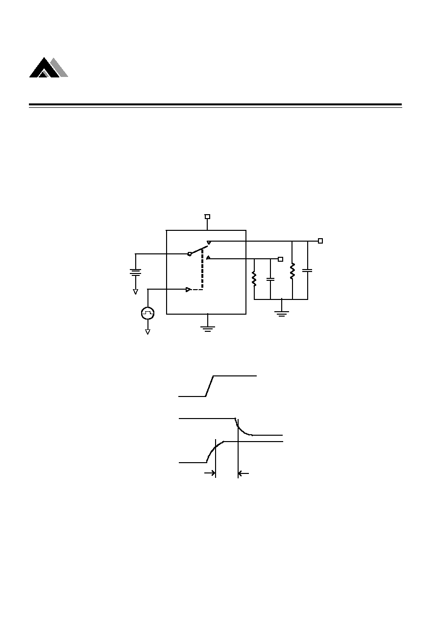
Timing Diagrams
Figure 1. Switching Time (AME4624 / AME4625)
V
OUT
t
OFF
Logic
Input
t
ON
OV
L
H
50%
0.9xV
IN
NO or NC
V
+
V
OUT
GND
Logic
Input
V
IN
IN
COM
R
L
C
L

AME, Inc.
7
AME4624/4625
1-Ohm Low Voltage
SPDT Analog Switch
n
Timing Diagrams (contd.)
Figure 2. Break-Before-Make Interval (AME4624)
V
OUT
Logic
Input
L
t
D
H
NC
V
+
V
OUT
GND
Logic
Input
V
IN
IN
COM
R
L
C
L
NO
AME, Inc.
8
AME4624/4625
1-Ohm Low Voltage
SPDT Analog Switch
n
Timing Diagrams (contd.)
Figure 3. Make-Before-Break Interval (AME4625)
Logic
Input
L
H
V
NC
V
NO
0.9xV
COM
0.9xV
COM
GND
V
COM
V
NC
C
L
V
+
Logic
Input
IN
R
L
C
L
NC
NO
COM
V
NO
R
L

AME, Inc.
9
AME4624/4625
1-Ohm Low Voltage
SPDT Analog Switch
n
Timing Diagrams
Figure 4. Channel Off / On Capacitance
NC or
NO
V+
V
INL
or
V
INH
GND
COM
IN
Capacitance
Meter
f=1MH
Z
V+
10nF

AME, Inc.
10
AME4624/4625
1-Ohm Low Voltage
SPDT Analog Switch
Ron vs. COM Voltage over Supply Voltage
Ron vs. COM Voltage over Temperature
OFF Leakage vs. Temperature
Charge Injection vs. COM Voltage(NC pin)
0
4
3
2
1
5
-50
-150
-200
0
50
V
COM
(V)
q
(
p
C
)
-100
100
AME4624
2
5
4
3
6
0.5
0
1.5
2.0
Supply Voltage (V)
L
o
g
i
c
T
h
r
e
s
h
o
l
d
V
o
l
t
a
g
e
(
V
)
1.0
2.5
IN ramping up
IN ramping down
Logic Threshold Voltage vs. Supply Voltage
0
4
3
2
1
5
6
5
4
3
1
2
8
7
9
V
COM
(V)
R
O
N
(
)
+1.8V
+2.0V
+2.5V
+2.3V
+5.0V
V
COM
=100mA
+3.0V
IN ramping down
2
5
4
3
6
10
0
30
40
V
SUPPLY
(V)
T
O
N
/
T
O
F
F
(
n
S
)
20
50
60
80
100
90
70
T
ON
T
OFF
TURN-ON/OFF Time vs. Supply Voltage
0
4
3
2
1
5
0.75
0.50
0.25
1.00
1.25
V
COM
(V)
R
O
N
(
)
T
A
=+105
0
C
T
A
=+85
0
C
T
A
=+25
0
C
T
A
=-40
0
C
T
A
=-55
0
C
-40
40
20
0
-20
60
1.0
0.8
0.0
1.4
1.6
Temperature (
O
C)
O
F
F
L
e
a
k
a
g
e
(
µ
A
)
80
100
0.2
0.4
0.6
1.2

AME, Inc.
11
AME4624/4625
1-Ohm Low Voltage
SPDT Analog Switch
-40
40
20
0
-20
60
30
25
0
45
50
Temperature (
O
C)
T
O
N
/
T
O
F
F
(
n
S
)
80
100
5
10
15
35
20
40
V+=5V
V
NO
or V
NC
=3V
T
ON
T
OFF
T
ON
/T
OFF
vs. Temperature

AME, Inc.
12
AME4624/4625
1-Ohm Low Voltage
SPDT Analog Switch
n
Date Code Rule
Year
A
A
A
W
W
xxx0
A
A
A
W
W
xxx1
A
A
A
W
W
xxx2
A
A
A
W
W
xxx3
A
A
A
W
W
xxx4
A
A
A
W
W
xxx5
A
A
A
W
W
xxx6
A
A
A
W
W
xxx7
A
A
A
W
W
xxx8
A
A
A
W
W
xxx9
Marking
Date Code
n
Tape & Reel Dimension
PIN 1
W
P
AME
AME
Package
Carrier Width (W)
Pitch (P)
Part Per Full Reel
Reel Size
SOT-26
8.0±0.1 mm
4.0±0.1 mm
3000pcs
180±1 mm
TSOT-26
8.0±0.1 mm
4.0±0.1 mm
3000pcs
180±1 mm
Carrier Tape, Number of Components Per Reel and Reel Size
AME, Inc.
13
AME4624/4625
1-Ohm Low Voltage
SPDT Analog Switch
n
Package Dimension
TSOT-26
Side View
L
1
Top View
S1
D
e
E
H
Front View
b
A
A
1
Side View
L
1
Top View
S1
D
e
E
H
Front View
b
A
A
1
SOT-26
MIN
MAX
MIN
MAX
A
A
1
0.00
0.15
0.0000
0.0059
b
0.30
0.55
0.0118
0.0217
D
2.70
3.10
0.1063
0.1220
E
1.40
1.80
0.0551
0.0709
e
H
2.60
3.00
0.10236 0.11811
L
1
0
o
10
o
0
o
10
o
S
1
0.37REF
0.0146REF
0.95REF
0.0374REF
1.90 BSC
0.0748 BSC
SYMBOLS
MILLIMETERS
INCHES
1.20REF
0.0472REF
MIN
MAX
MIN
MAX
A+A
1
0.90
1.25
0.0354
0.0492
b
0.30
0.50
0.0118
0.0197
c
0.09
0.25
0.0035
0.0098
D
2.70
3.10
0.1063
0.1220
E
1.40
1.80
0.0551
0.0709
e
H
2.40
3.00
0.09449 0.11811
L
1
0
o
10
o
0
o
10
o
S
1
1.90 BSC
0.07480 BSC
SYMBOLS
MILLIMETERS
INCHES
0.35BSC
0.0138BSC
0.95BSC
0.0374BSC

Life Support Policy:
These products of AME, Inc. are not authorized for use as critical components in life-support devices or sys-
tems, without the express written approval of the president
of AME, Inc.
AME, Inc. reserves the right to make changes in the circuitry and specifications of its devices and
advises its customers to obtain the latest version of relevant information.
©
AME, Inc. , November 2005
Document: 2079-DS4624/4625-G
Corporate Headquarter
U.S.A.(Subsidiary)
AME, Inc.
Analog Microelectronics, Inc.
2F, 302 Rui-Guang Road, Nei-Hu District
3100 De La Cruz Blvd., Suite 201
Taipei 114, Taiwan .
Santa Clara, CA. 95054-2046
Tel: 886 2 2627-8687
Tel : (408) 988-2388
Fax: 886 2 2659-2989
Fax: (408) 988-2489
www.ame.com.tw
E-Mail: sales@ame.com.tw