
ASAHI KASEI [AK4532]
0178-E-01 1 1999/06
AK4532
Internet/Network/General Purpose Multimedia Audio CODEC
General Description
The AK4532 is a low-cost high-quality 16-Bit CODEC designed specifically for Internet Boxes, Network
PCs, and to interface with audio/video controller ICs for standard PC applications. AKM's AK4532
serial interface mode simplifies the design process on existing and new audio projects. The converters
can have a range of 4 to 50 kHz. For voice mail applications, an internal 26 dB microphone preamp has
been added and because of the internal input mixer, music or other sounds can easily be mixed with voice.
Features
ñ
2ch Audio CODEC
ñ
2ch stereo including 1ch mono recording mixer with L/R, R/L, L/L and R/R switching
ñ
2ch stereo playback mixer
ñ
Mic input with 26 dB optional gain
ñ
High Jitter Tolerance
ñ
Interface compatible with AKM's AK4531
ñ
Sampling Rate: 4 kHz to 50 kHz
ñ
3-wire Serial Interface for Mixer Control
ñ
5 V operation, can connect to 3.3 V Digital Controller.
ñ
Low power consumption - 150 mW
ñ
Power down mode
ñ
Small low profile package - 24 pin VSOP.
Block Diagram

ASAHI KASEI [AK4532]
0178-E-01 2 1999/06
Ordering Guide
AK4532 from -10
¯
C to +70
¯
C 24pin VSOP(0.65mm pitch)
AKD4532 Evaluation Board
Pin Layout

ASAHI KASEI [AK4532]
0178-E-01 3 1999/06
Pin and Function
Pin
Pin Name
I/O
Function
1
AGND
-
Analog Ground
2
VA
-
Analog Power - 5V
3
MIC/AUXR
I
Mic or Right Aux Line Level Input
4
AUXL
I
Left Aux Line Level Input
5
LINER
I
Right Line Level Input
6
LINEL
I
Left Line Level Input
7
PD
I
Power down and Reset
8
MCLK
I
Master Clock for CODEC
9
LRCK
I
Left Right Clock for CODEC
10
SCLK
I
Serial Clock for CODEC
11
SDI
I
Serial Data In
12
SDO
O
Serial Data Out
13
DGND
-
Digital Ground
14
VD
-
Digital Power - 5V
15
CS
I
Chip Select
16
CCLK
I
Control Port Clock
17
CDATA
I
Control Port Data
18
CMODE
I
MCLK select (L:256fs, H:384fs)
19
LOUT
O
Left Analog Out
20
ROUT
O
Right Analog Out
21
VRAD
I
A/D Reference
Connect to AGND with 0.1uF and 4.7uF capacitors
22
AINFL
-
L channel Antialias Filter Pin
Connect to AGND with 1.0nF capacitor
23
AINFR
-
R channel Antialias Filter Pin
Connect to AGND with 1.0nF capacitor
24
VCOM
-
Voltage Common Output Pin
Connect to AGND with 0.1uF and 4.7uF capacitors.
Note: 1. No load current may be taken from the VCOM, VRAD pins for the external circuits.
2. All digital input pins should not be left floating.
ASAHI KASEI [AK4532]
0178-E-01 4 1999/06
ABSOLUTE MAXIMUM RATINGS
AGND, DGND = 0 V
Parameter
Symbol
min
max
Units
Power Supplies:
Analog
Digital
VA
VD
-0.3
-0.3
6.0
6.0 or VA+0.3
V
V
Input Current, Any Pin except Supplies
IIN
-
+/- 10
mA
Analog Input Voltage Range
VINA
-0.3
6.0 or VA+0.3
V
Digital Input Voltage
VIND
-0.3
6.0 or VA+0.3
V
Ambient Temperature
Ta
-10
70
Storage Temperature
Tstg
-65
150
Note: 1. All voltages with respect to ground.
2. Max value is higher voltage of 6.0 or VA+0.3V.
WARNING: Operation at or beyond these limits may result in permanent damage to the device. Normal
Operating Specifications are not guarantee at these extremes.
RECOMMENDED OPERATING CONDITIONS
(AGND, DGND = 0 V, Note 1)
Parameter
Symbol
min
typ
max
units
Power Supplies
Analog
Digital
VA
VD
4.5
4.5
5.0
5.0
5.5
VA
V
V
Note 1: All voltages with respect to ground.

ASAHI KASEI [AK4532]
0178-E-01 5 1999/06
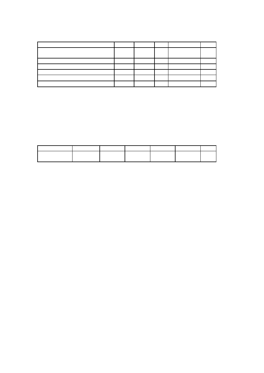
ANALOG CHARACTERISTICS
(Ta=25 ; VA, VD = 5.0V; fs = 44.1kHz; Signal Frequency = 1 kHz; MCLK=256fs; BCLK = 64 fs;
LRCK = fs, Gain, ATT and Mixer switches are defualt setting. Measurement frequency bandwidth is
10Hz to 20kHz, unless otherwise noted.)
Parameter
min
typ
max
units
A/D
measured via LineL and LineR
Resolution
16
Bits
S/(N+D)
-0.5 dB Input
74
80
dB
S/N
A-weighted
84
90
dB
Dynamic Range
-60 dB Input,
A-weighted
84
90
dB
Interchannel Isolation
(Note 1)
68
76
dB
Interchannel Gain Mismatch
0.2
0.5
dB
Gain Drift
100
ppm/
Offset Error
(Note 2)
+/- 1
LSB
Input Voltage
(Note 4)
2.50
2.70
2.90
Vpp
Mixer Input Resistance
30
60
100
k
D/A
measured via LOUT and ROUT
Resolution
16
Bits
S/(N+D)
75
83
dB
S/N
A-weighted
83
87
dB
Dynamic Range
-60 dB Input,
A-weighted
83
87
dB
Interchannel Isolation
(Note 1)
80
100
dB
Interchannel Gain Mismatch
0.2
0.7
dB
Gain Drift
100
ppm/
Output Voltage
(Note 4)
2.85
3.05
3.35
Vpp
Load Resistance
10
k
Out-of-Band Noise
BW < 100 kHz
-81
dB
MIC Amp
Gain
24
26
28
dB
Input Resistance
For 26dB setting
15
25
40
k
Mixer Gain Control
32 Steps
Step Size
(Note 3)
0
2
dB
Gain Control Range
-50
12
dB
Master Volume
32 Steps
Step Size
(Note 3)
0
2
dB
Attenuation Control Range
-62
0
dB
Power Supplies
Normal Operation
VA
27
40
mA
VD
3
5
mA
Power Dissipation
150
225
mW
Power-Down Mode
VA
10
uA
VD
10
uA
Power Dissipation
100
200
uW
Note: 1. Crosstalk between channels on the same A/D or D/A.
2. Internal HPF removes offset.
3. Minimum spec applies to -40dB setting.
4. Input and Output voltage scale with VA.

ASAHI KASEI [AK4532]
0178-E-01 6 1999/06
FILTER CHARACTERISTICS
(Ta=25 ; VA, VD = 5.0VÝ10%; fs = 44.1 kHz)
Parameter
Symbol
min
typ
max
Units
A/D Digital Filter
(Decimation LPF)
Passband (Note 1)
+/- 0.1 dB
-0.5 dB
-1.2 dB
-6.7 dB
PB
0
0
0
0
16.5
19.0
20.0
22.05
kHz
kHz
kHz
kHz
Stopband
SB
26.0
kHz
Passband Ripple
PR
+/- 0.1
dB
Stopband Attenuation
SA
68
dB
Group Delay Distortion
Delta GD
0
uS
Group Delay (Note 2)
GD
16.1
1/fs
A/D Digital Filter (HPF)
Frequency Response
(Note 1)
-3 dB
-0.5 dB
-0.1 dB
FR
6.85
19.6
44.9
Hz
Hz
Hz
D/A Digital Filter
Passband (Note 1)
+/- 0.1 dB
-6.0 dB
PB
0
0
18.0
22.05
kHz
kHz
Stopband
SB
26.1
kHz
Passband Ripple
PR
+/- 0.1
dB
Stopband Attenuation
SA
65
dB
Group Delay (Note 2)
GD
14.4
1/fs
D/A Digital Filter
+ Analog Filter
Frequency Response
0 to 20 kHz
FR
+/- 1.0
dB
Note: 1. The passband and stopband frequencies scale with fs.
2. The calculating delay time which occurred by digital filtering. This time is from the input of
analog signal to setting the 16bit data of both channels to the output register of ADC.
For DAC, this time is from setting 16bit data of both channels on input register to the output of
analog signal.
DIGITAL CHARACTERISTICS
(Ta=25 ; VA, VD = 5.0VÝ10%)
Parameter
Symbol
min
typ
max
Units
High-Level Input Voltage
Low-Level Input Voltage
VIH
VIL
2.2
-
-
-
-
0.8
V
V
High-Level Output Voltage (Iout=-80uA)
Low-Level Output Voltage (Iout=80uA)
VOH
VOL
VD-0.4
-
-
-
-
0.4
V
V
Input Leakage Current
Iin
-
-
+/-10
uA

ASAHI KASEI [AK4532]
0178-E-01 7 1999/06
SWITCHING CHARACTERISTICS
(Ta=25 ; VA, VD = 5.0VÝ10%, Cl = 20pF)
Parameter
Symbol
min
typ
max
Units
Master Clock Timing (CMODE=L)
(CMODE=H)
Pulse Width Low (CMODE=L)
(CMODE=H)
Pulse Width High (CMODE=L)
(CMODE=H)
fCLK
fCLK
fCLKL
fCLKL
fCLKH
fCLKH
1.024
1.536
31.25
23
31.25
23
11.2896
16.9344
12.800
19.2
MHz
MHz
ns
ns
ns
ns
LRCK Frequency (Note 1)
Duty Cycle
fs
4
45
44.1
50
55
kHz
%
Serial Interface Timing
SCLK Period
SCLK Pulse Width Low
SCLK Pulse Width High
LRCK Edge to SCLK "rising edge" (Note 2)
SCLK "rising edge" to LRCK edge (Note 2)
SDI Hold Time
SDI Setup Time
LRCK to SDO(MSB)
SCLK "rising edge" to SDO
tSCK
tSCKL
tSCKH
tLRS
tSLR
tSDH
tSDS
tLRS
tSSD
312.5
100
100
50
50
50
50
70
70
ns
ns
ns
ns
ns
ns
ns
ns
ns
Control Interface Timing
CCLK Period
CCLK Pulse Width Low
CCLK Pulse Width High
CDATA Hold Time
CDATA Setup Time
CS
High Level Time
CS
"falling edge" to CCLK "rising" time
CCLK "rising time" to
CS
"rising" time
tCCK
tCCKL
tCCKH
tCDS
tCDH
tCSW
tCSS
tCSH
200
80
80
50
50
150
50
50
ns
ns
ns
ns
ns
ns
ns
ns
Reset Timing
PD
Pulse Width
PD
"rising edge" to SDO delay (Note 3)
tPD
tPDS
150
516
ns
1/fs
Note: 1. If the duty of LRCK changes larger than 5% from 50%, the AK4532 is reset by the internal phase
detecting circuit automatically.
2. SCLK rising edge must not occur at the same time as LRCK edge.
3. These cycles are the number of LRCK rising from
PD
rising.

ASAHI KASEI [AK4532]
0178-E-01 8 1999/06
Audio Data Formats
The data format of ADC and DAC are MSB first & MSB justified with 16bit. The SCLK needs 32fs or
more than 32fs in a LRCK cycle.
15
1
141312
0
15
1
141312
0
1514
Don't Care
Don't Care
SCLK
SDI
16Bit
Lch
Rch
15
1
141312
0
15
1
141312
0
1514
Don't Care
Don't Care
SDO
16Bit
SDO,SDI - 15:MSB,0:LSB
LRCK
=64fs
Timing Diagram
VIH
VIL
LRCK
SCLK
MCLK
tCLKL
1/fCLK
t
CLKH
VIH
VIL
1/fs
VIH
VIL
t
SCKL
t
SCK
t
SCKH
Clock Timing
LRCK
SCLK
SDO
t
SSD
VIH
VIL
VIH
VIL
VIH
VIL
t
LRS
t
SLR
t
SDH
t
SDS
SDI
VIH
VIL
t
LRS
Serial Audio Interface Timing

ASAHI KASEI [AK4532]
0178-E-01 9 1999/06
CS
CCLK
CDATA
A6
A7
A5
t
CSS
t
CCKH
t
CCKL
t
CCK
t
CDS
t
CDH
VIH
VIL
VIH
VIL
VIH
VIL
t
CSW
Control Data Interface Timing 1
CS
CCLK
CDATA
D0
D1
t
CSH
VIH
VIL
VIH
VIL
VIH
VIL
D2
Control Data Interface Timing2
VIL
PD
tPD
Power down and Reset Timing

ASAHI KASEI [AK4532]
0178-E-01 10 1999/06
OPERATION OVERVIW
1. CONTROL REGISTER MAP
Addr
Register Name
D7
D6
D5
D4
D3
D2
D1
D0
00
Master Volume Lch
MUTE
ATT4
ATT3
ATT2
ATT1
ATT0
01
Master Volume Rch
MUTE
ATT4
ATT3
ATT2
ATT1
ATT0
02
Voice Volume Lch
MUTE
GAI4
GAI3
GAI2
GAI1
GAI0
03
Voice Volume Rch
MUTE
GAI4
GAI3
GAI2
GAI1
GAI0
08
Line Volume Lch
MUTE
GAI4
GAI3
GAI2
GAI1
GAI0
09
Line Volume Rch
MUTE
GAI4
GAI3
GAI2
GAI1
GAI0
0A
AUX Volume Lch
MUTE
GAI4
GAI3
GAI2
GAI1
GAI0
0B
AUX Volume Rch
MUTE
GAI4
GAI3
GAI2
GAI1
GAI0
10
Output Mixer SW 1
LineL
LineR
MIC
11
Output Mixer SW 2
AUXL
AUXR
VoiceL
VoiceR
12
Lch Input Mixer SW 1
LineL
LineR
13
Rch Input Mixer SW 1
LineL
LineR
14
Lch Input Mixer SW 2
AUXL
AUXR
VoiceL
15
Rch Input Mixer SW 2
AUXL
AUXR
VoiceR
16
Reset and Power Down
PD
RST
19
MIC Amp Gain
MGAIN
Note: ATT* is data bits for the attenuation level.
GAI* is data bits for the gain level.
IMPORTANT: There is the compatibility between the AK4531 and AK4532. But the input mixer
functions of those device has some different implication in the application, receptively.
And the other address of control register except those described in the above table and "1A" are
"do not care". Address "1A" for testing shall be strictly prohibited to access.
Be ware that the three MSB address bits(A7, A6, A5) are ignored by AK4532. Writing to address
"20" register will update the address "00" register for instance.
2. WRITE Timing of Control Register
CS
CCLK
1
A7-A0:
Address
D7-D0:
Control Data
3
4
5
6
7
9
10
11
12
13
14
15
2
8
CDATA
D0
D1
D2
D3
D4
D5
D6
A0
A1
A2
A3
A4
A6
A7
A5
D7
0
3. Control Register Definitions
Addr
Register Name
D7
D6
D5
D4
D3
D2
D1
D0
00
Master Volume Lch
MUTE
ATT4
ATT3
ATT2
ATT1
ATT0
01
Master Volume Rch
MUTE
ATT4
ATT3
ATT2
ATT1
ATT0
MUTE
1:
MUTE
0:
No MUTE
ATT4:0
32 levels with 2 dB step
00000: 0dB
11111: -62 dB
Initial "0000 0000"(No MUTE & 0dB)

ASAHI KASEI [AK4532]
0178-E-01 11 1999/06
Addr
Register Name
D7
D6
D5
D4
D3
D2
D1
D0
02
Voice Volume Lch
MUTE
GAI4
GAI3
GAI2
GAI1
GAI0
03
Voice Volume Rch
MUTE
GAI4
GAI3
GAI2
GAI1
GAI0
08
Line Volume Lch
MUTE
GAI4
GAI3
GAI2
GAI1
GAI0
09
Line Volume Rch
MUTE
GAI4
GAI3
GAI2
GAI1
GAI0
0A
AUX Volume Lch
MUTE
GAI4
GAI3
GAI2
GAI1
GAI0
0B
AUX Volume Rch
MUTE
GAI4
GAI3
GAI2
GAI1
GAI0
MUTE
1:
MUTE
0:
No MUTE
ATT4:0
32 levels with 2 dB step
00000: 12dB
00110: 0 dB
11111: -50 dB
Initial "0000 0110"(No MUTE & 0dB)
Addr
Register Name
D7
D6
D5
D4
D3
D2
D1
D0
10
Output Mixer SW 1
LineL
LineR
MIC
11
Output Mixer SW 2
AUXL
AUXR
VoiceL
VoiceR
12
Lch Input Mixer SW 1
LineL
LineR
13
Rch Input Mixer SW 1
LineL
LineR
14
Lch Input Mixer SW 2
AUXL
AUXR
VoiceL
15
Rch Input Mixer SW 2
AUXL
AUXR
VoiceR
ON/OFF of Mixer Switches
0:
OFF
1:
ON
Initial
"000X XX00"
XXX=000: Addr=10,14,15 (All:OFF)
XXX=011: Addr=11(Output Mixer Voice R&L:ON)
XXX=100: Addr=12(Lch Input Mixer Line L :ON)
XXX=010: Addr=13(Rch Input Mixer Line R :ON)
Addr
Register Name
D7
D6
D5
D4
D3
D2
D1
D0
16
Reset and Power Down
PD
RST
19
MIC Amp Gain
MGAIN
RST
initializes the contents of all registers except
PD
and
RST
registers. When
PD
pin goes low,
RST
register becomes
"1".
1: Normal Operation
0: Initialize
PD
register enables the power down. When
PD
pin goes low,
PD
register becomes "1".
1: Normal Operation
0: Power Down
MGAIN selects the gain of MIC amp. The initial state is "0".
0: Bypass (0dB)
1: 26 dB
Try to avoid pops and clicks when activating or inactivating this function.

ASAHI KASEI [AK4532]
0178-E-01 12 1999/06
4. Explanation of each sequence
4.1. Reset & Power down
INIT1
INITA
Normal
PD
Normal
INIT2
Normal PD+INIT2
Normal
Inhibit(1)
Inhibit(2)
Inhibit(2
Power Supply
PD pin
PD(register)
RST(register)
Internal State
Write to register
External clock
MCLK,LRCK,SCLK
The clocks may be stopped.
INITA
INITA
INIT1: Initializing all registers. The AK4532 exists in the power down state.
INIT2: Initializing all registers except
PD
,
RST
registers.
INITA: Initializing the analog section. Initializing period is 516/fs.
PD: Power down state. All analog outputs are floating.
In case of
RST
register = "0", initializing all registers except
PD
,
RST
registers.
Inhibit(1): Inhibits writing to all registers.
Inhibit(2): Inhibits writing to all registers except for
PD
,
RST
registers.
The AK4532 operates with the external clocks(MCLK, LRCK, SCLK) during initializing the
analog section.
Figure 1. Reset & Power Down Sequence
4.2.
PD
pin operation
"H": Normal operation
"L": Initializing mode 1(INIT1 in Figure 1)
Initializing all registers.
Inhibits writing to all registers.
The initialization of the analog section starts at rising edge of
PD
pin.
SDO pin stays "L" during the initializing periods of 516/fs.
Going into power down state.
4.3.
RST
register operation
"1": Normal operation
"0": Initializing mode 2(INIT2 in Figure 1)
Initializing all registers except
PD
,
RST
registers.
Inhibits writing to all registers except
PD
,
RST
registers.
RST
register goes "1" when
PD
pin goes "L".
The analog section is not initialized.
4.4.
PD
register operation
"1": Normal operation
"0": Power down
The contents of all registers are held.
PD
resister goes "1" when
PD
pin goes "L"
.
All analog outputs(LOUT, ROUT) go floating.
The initialization of the analog section starts at the rising edge of
PD
resister.
SDO pin stays "L" during the initializing period of 516/fs.
4.5. SDO output pin operation

ASAHI KASEI [AK4532]
0178-E-01 13 1999/06
SDO output is the 16bit data of ADC and goes "L"(0000H) in the following cases.
PD
pin = "L"
During initializing the analog section(516/fs).
RST
register = "0"
PD
register = "0"
4.6. Analog output pin(LOUT, ROUT) operation
These outputs are floating in the following case.
PD
pin = "L"
PD
register = "0"
5. System Clock
The external clocks which are required to operate the AK4532 are MCLK, LRCK and SCLK. MCLK
should be synchronized with LRCK but the phase is free of care. As the AK4532 includes the phase
detect circuit for LRCK, the AK4532 is reset automatically when the synchronization is out of phase
by changing the clock frequencies. Therefore, the reset is not required except only upon power-up.
All external clocks should always be present whenever the AK4532 is in normal operation mode. If these
clocks are not provided, the AK4532 may draw excessive current and do not possibly operate
properly because the device utilizes the dynamic logic internally. If the external clocks are not
present, the AK4532 should be in the power down mode.
5. Digital High Pass Filter
The ADC of the AK4532 has a digital high pass filter for DC offset cancel. The cut-off frequency of
the HPF is 6.85Hz at fs=44.1kHz and the frequency response at 20Hz is -0.5dB. It also scales with
sampling rate(fs).

ASAHI KASEI [AK4532]
0178-E-01 14 1999/06
System Design
Figure 2 shows the system connection diagram. An evaluation board is available which demonstrates the
optimum layout, power supply arrangements and measurement results.
PD
LRCK
DGND
AGND
VD
Synth.
Controller
+5V
Analog
VA
AK4532
LOUT
0.1u
0.1u
4.7u
4.7u
+
+
VRAD
SCLK
SDI
Analog
Out
Lch
4.7u
+
0.1u
ROUT
Analog
Out
Rch
VCOM
CMODE
CDATA
CCLK
CS
13
1
19
20
7
9
10
11
18
17
16
15
24
2
14
MCLK
8
SDO
12
&
4.7u
+
0.1u
21
AINFL
22
MIC/AUXR
3
AUXL
4
LineR
5
LineL
6
AINFR
23
10
Figure 2. Typical Connection Diagram
1. Grounding and power supply decoupling
The AK4532 requires careful attention to power supply and grounding arrangements. VD should be
supplied from analog power supply. Analog ground and digital ground should be connected together
near to where the supplies are brought onto the printed circuit board. Decoupling capacitors should
be as near to the AK4532 as possible, with the small value ceramic capacitor being the nearest.
2. On-chip voltage reference
The on-chip voltage references are output on the VRAD and VCOM pins for decouping .
The VRAD is used as the reference of A/D conversion. The VCOM is a signal ground of this chip. An
electrolytic capacitor less than 10uF in parallel with a 0.1uF ceramic capacitor attached to these pins
eliminates the effects of high frequency noise. Especially, the small value ceramic capacitors should
be as near to the AK4532 as possible. No load current may be drawn from the VRAD and VCOM
pins. All signals, especially clocks, should be kept away from the VRAD and VCOM pins in order to
avoid unwanted coupling into the chip.

ASAHI KASEI [AK4532]
0178-E-01 15 1999/06
3. Analog Inputs
The mixer input and the ADC inputs are single-ended and internally biased to the VCOM voltage with
60k(typ) resistance. The input signal range is typically 2.83Vpp(1Vrms). Figure 3 is an example
for 2Vrms line-level input circuit. The ADC output data format is 2's complement. The AK4532
accepts input voltages from AGND to VA. The output code is 7FFFH for input above a positive full
scale and 8000H for input below a negative full scale. The ideal code is 0000H with no input signal.
The DC offset is canceled by the internal HPF.
LINE/AUX
0.47u
5.1k
AK4532
Analog
Input
2Vrms
5.1k
Figure 3. 2Vrms Line-level Input
The AK4532 samples the analog inputs at 64fs. The digital filter rejects all noise higher than the stop
band. However, the filter will not reject frequencies right around 64fs(and multiples of 64fs). Most
audio signals do not have significant energy at 64fs. As a result, two 1nF capacitors are necessary for
AINFR and AINFL.
4. Analog Outputs
The analog outputs are also single-ended and centered around the VCOM voltage. The output signal
range is typically 2.83Vpp(1Vrms). The DAC input data format is 2's complement. The output
voltage is a positive full scale for 7FFFH and a negative full scale for 8000H. The ideal output is
VCOM voltage for 0000H. The internal switched-capacitor filter and continuous-time filter almost
remove the noise generated by the delta-sigma modulator of DAC beyond the audio passband,
especially low sampling rate. The noise floor level is almost constant and the audible noise level is
-83dB(typ) at 8kHz sampling.
5. Other information
5.1 Clock change
The clock change or LRCK phase shift should be done while muting the DAC output by the master
volume or voice volume to avoid the click noise by out-of-synchronization.
ADC may output digital code at the clock change, or LRCK phase shift may produce incomplete or
destroyed 16bit data. Then some attention is required carefully.
5.2 Offset on mixer inputs
When the mixer gain is set to +12dB, the output has pretty large offset even if the inputs are no signal.
Therefore, large click noise may occur when the gain level is changed quickly.
5.3 Click noise on the analog outputs
The click noise of about -50dB occurs from the analog outputs(LOUT, ROUT) at the power on/off or the
transition of
PD
register. The analog outputs should be muted externally if the click noise influences
systems application.

ASAHI KASEI [AK4532]
0178-E-01 16 1999/06
Package
0.65
0.22Ý0.1
*
7.8 Ý0.15
0.15Ý0.05
1.25Ý0.2
*
5.
6
Ý
0.
2
0.1
7.
6
Ý
0.
2
0
.
5
Ý
0.
2
010
1
12
24
13
24pin VSOP
(Unit: mm)
0.10
Detail
Seating Plane
NOTE: Dimension "*" does not include mold flash.
Package & Lead frame materiel
Package molding compound : Epoxy
Lead frame material :Cu
Lead frame surface treatment : Solder plate

ASAHI KASEI [AK4532]
0178-E-01 17 1999/06
Marking
A K 4 5 3 2 V F
A A X X X X
1) Pin #1 indication
2) AA: LOT#
3) Date Code: XXXXX(4 digits)
4) Marketing Code: AK4532-VF
5) Country of Origin
6) Asahi Kasei Logo