
AIC1574
5-bit DAC, Synchronous PWM Power Regulator
with Triple Linear Controllers
Analog Integrations Corporation 4F, 9, Industry E. 9th Rd, Science Based Industrial Park, Hsinchu Taiwan, ROC
www.analog.com.tw
DS-1574-00 May 22, 01
TEL: 886-3-5772500 FAX: 886-3-5772510
1
n
FEATURES
l
Compatible with HIP6021.
l
Provides 4 Regulated Voltages for Microprocessor
Core, AGP Bus, Memory and GTL Bus Power.
l
TTL Compatible 5-bit Digital-to-Analog Core Output
Voltage Selection. Range from 1.3V to 3.5V.
0.1V Steps from 2.1V to 3.5V.
0.05V Steps from 1.3V to 2.05V.
l
�
1.0% Output Voltage for VCORE,
�
3.0% Accu-
racy for Linear Controller Outputs.
l
Simple Voltage-Mode PWM Control and Built in
Internal Compensation Networks.
l
N-Channel MOSFET Driver for PWM Buck Con-
verter.
l
Linear Controller Drives Compatible with both N�
Chanel MOSFET and NPN Bipolar Series Pass
Transistor.
l
Operates from +3.3V, +5V and +12V Inputs.
l
Fast Transient Response.
l
Full 0% to 100% Duty Ratios.
l
Adjustable Current Limit without External Sense
Resistor.
l
Microprocessor Core Voltage Protection against
Upper MOSFET shorted to +5V.
l
Power Good Output Voltage Monitor.
l
Over-Voltage and Over-Current Fault Monitors.
l
200KHz Free-Running Oscillator Programmable up
to 700KHz.
n
APPLICATIONS
l
Full Motherboard Power Regulation for Computers.
n
DESCRIPTION
The AIC1574 combines a synchronous voltage mode
controller with three linear controller as well as the
monitoring and protection functions in this chip. The
PWM controller regulates the microprocessor core
voltage with a synchronous rectified buck converter.
The three linear controllers regulate power for the
1.5V or 3.3V AGP bus power, the 1.5V GTL bus and
the 1.8V power for the chip set core voltage and/or
cache memory circuits.
An integrated 5 bit D/A converter that adjusts the
core PWM output voltage from 2.1V to 3.5V in 0.1V
increments and from 1.3V to 2.05V in 0.05V incre-
ments. The linear controller for AGP bus power is
selectable by TTL-compatible SELECT pin status for
1.5V or 3.3V with
�
3% accuracy. The other two
linear controller provide 1.5V
�
3% and 1.8V
�
3% or
adjustable output voltage by means of external di-
vided resistor based on FIX pin status.
This chip monitors all the output voltages. Power
Good signal is issued when the core voltage is
within �10% of the DAC setting and the other levels
are above their under-voltage levels. Over-voltage
protection for the core output uses the lower N-
channel MOSFET to prevent output voltage above
116% of the DAC setting.
The PWM over-current function monitors the output
current by using the voltage drop across the upper
MOSFET's R
DS(ON)
, eliminating the need for a cur-
rent sensing resistor
.

AIC1574
2
n
TYPICAL APPLICATION
+
+
+
VAUX
DRIVE2
VSEN2
SELECT
DRIVE3
VSEN3
SD
DRIVE4
VESN4
FIX
2
9
11
10
16
COUT2
Q3
+3.3VIN
3.3V or 1.5V
VOUT2
+12VIN
10
2.2
�
F
COUT4
1.8V
Q5
Q4
COUT3
14
VOUT4
15
VOUT3
19
18
1.5V
1
GND
28
23
VCC
17
7
6
5
4
3
8
13
12
20
21
22
24
25
26
27
+
+
UGATE1
PHASE1
LGATE1
PGND
VSEN1
FB
NC
VID0
VID1
VID2
VID3
VID4
PGOOD
FAULT/RT
SS
COUT1
Css
OCSET1
L1
GND
+5VIN
D5820
1
�
H
L1
Q2
Q1
VOUT1

AIC1574
3
n
ORDERING INFORMATION
ORDER NUMBER
PIN CONFIGURATION
AIC1574-CX
AIC157 4CS
(SO28)
PACKAGING TYPE
S: SMALL OUTLINE
1
3
4
2
5
7
6
8
9
10
VID 1
FIX
VID 4
VID 3
DRIVE2
VID 2
VSEN2
VID0
SD
PGOOD
11
12
SS
SELECT
PHASE1
VCC
UGATE1
OCSET
LGATE1
PGND
20
19
VSEN1
VSEN3
FB
NC
28
26
27
25
24
23
21
22
18
17 GND
DRIVE3
13
14
VSEN4
FAULT/RT
16
15 DRIVE4
VAUX
n
ABSOLUTE MAXIMUM RATINGS
Supply Voltage, V
CC
.................. ... ... ... ... ........ ... ... ... ...... ... ...... ..... ... ..................... +15V
PGOOD, FAULT and GATE Voltage ...... ... ... ... ........ ... ... ..... .... GND -0.3V to V
CC
+0.3V
Input, Output , or I/O Voltage
......... ...... ... ... ... ... ... ... ... ..... ... ............ GND -0.3V to 7V
Recommended Operating Conditions
Supply Voltage; VCC... ... .................. ... ... ... ..................... +12V�10%
Ambient temperature Range ... ... ..... ... ... ... ... ... ................. 0
�
C~70
�
C
Junction Temperature Range ... ... ......... ..... ... .................. 0
�
C~125
�
C
Thermal Information
Thermal Resistance,
JA
SOIC package ... ... ... ... ... ... ... ... ... ... ... ..... ... ..... ... .............. 70
�
C/W
SOIC package (with 3in
2
of copper) ... ...... ... ... ............ ......... 50
�
C/W
Maximum Junction Temperature (Plastic Package) ... ... ... ... ... ... ... ..... ... ...... 150
�
C
Maximum Storage Temperature Range
... ... ... ... ... ... ... ... ... ... ... .... -65
�
C ~ 150
�
C
Maximum Lead Temperature (Soldering 10 sec)
... ... ... ... ... ... ... ... ... ... ..... ... 300
�
C
n
TEST CIRCUIT
Refer to APPLICATION CIRCUIT.

AIC1574
4
n
ELECTRICAL CHARACTERISTICS
(Vcc=12V, TJ=25
�
C, Unless otherwise specified)
PARAMETER
TEST CONDITIONS
SYMBOL
MIN.
TYP.
MAX.
UNIT
VCC SUPPLY CURRENT
Supply Current
UGATE, LGATE, GATE3 and
VOUT2 open
I
CC
3
mA
POWER ON RESET
Rising VCC Threshold
VOCSET=4.5V
V
CCTHR
10.4
V
Falling VCC Threshold
VOCSET=4.5V
V
CCTHF
8.2
V
Rising VAUX Threshold
VAUX
THR
2.5
V
VAUX Threshold Hysteresis
VAUX
HYS
500
mV
Rising VOCSET1 Threshold
V
OCSETH
1.26
V
OSCILLATOR
Free Running Frequency
RT=Open
F
170
200
230
KHz
Total Variation
6k
<RT to GND<200k
-15
+15
%
Ramp. Amplitude
RT=open
V
OSC
1.5
VP-P
REFERENCE AND DAC
DAC (VID0~VID4) Input Low
Voltage
V
IDL
0.8
V
DAC (VID0~VID4) Input High
Voltage
V
IDH
2.0
V
DACOUT Voltage Accuracy
V
DAC
=1.8V~3.5V
-1.0
+1.0
%
Bandgap Reference Voltage
V
REF
1.265
V
Bandgap Reference Toler-
ance
-2.5
+2.5
%
LINEAR REGULATOR (OUT2, OUT3, OUT4)
Regulation
3
%
VSEN2 Regulation Voltage
Select<0.8V
V
REG2
1.5
V
VSEN2 Regulation Voltage
Select>2.0V
V
REG2
3.3
V
VSEN3 Regulation Voltage
V
REG3
1.5
V
VSEN3 Regulation Voltage
V
REG4
1.8
V
Under-Voltage Level
( V
SEN
/V
REG
)
V
SEN
Rising
V
SENUV
75
%
Under-Voltage Hysteresis
(V
SEN
/V
REG
)
V
SEN
Falling
5
%
Output Drive Current (All
Linears )
V
AUX
-V
DRIVE
> 0.6V
20
30
mA

AIC1574
5
n
ELECTRICAL CHARACTERISTICS
(Continued)
PARAMETER
TEST CONDITIONS
SYMBOL MIN.
TYP.
MAX.
UNIT
SYNCHRONOUS PWM CONTROLLER AMPLIFIER
DC Gain
(G.B.D.)
80
dB
Gain-Bandwidth Product
(G.B.D.)
G
BWP
13
MHz
Slew Rate
(G.B.D.) note 1.
S
R
6
V/
�
s
PWM CONTROLLER GATE DRIVER
Upper Drive Source
V
CC
=12V, V
UGATE
= 6V
I
UGH
0.9
A
Upper Drive Sink
V
UGATE
=1V
R
UGL
2.8
3.5
Lower Drive Source
V
CC
=12V, V
LGATE
=6V
I
LGH
1
A
Lower Drive Sink
V
LGATE
=1V
R
LGL
2.2
3.0
PROTECTION
VSEN1 Over-Voltage
( V
SEN1
/D
ACOUT
)
V
SEN1
Rising
OVP
116
120
%
FAULT Sourcing Current
V
CC
-
V
FAULT/RT
=2.0V
I
OVP
20
mA
OCSET Current Source
V
OCSET
=4.5VDC
I
OCSET
170
200
230
�
A
Soft-Start Current
I
SS
25
�
A
POWER GOOD
V
SEN1
Upper Threshold
( V
SEN1
/DA
COUT
)
V
SEN1
Rising
108
111
%
V
SEN1
Under-Voltage
( VSEN1/DACOUT )
V
SEN
Falling
92
95
%
V
SEN1
Hysteresis
(VSEN1/DACOUT)
Upper and Lower Threshold
2
%
P
GOOD
Voltage Low
I
PGOOD
=-4mA
V
PGOOD
0.4
0.8
V
Note 1. Without internal compensation network, the gain bandwidth product is 13MHz. Being associated with in-
ternal compensation networks, the Bode Plot is shown in Fig. 3, "Internal Compensation Gain of PWM Error Am-
plifier".

AIC1574
6
n
TYPICAL PERFORMANCE CHARACTERISTICS
PGOOD
V
OUT4
V
OUT3
SS
V
OUT2
V
OUT1
Fig. 1 Soft Start Interval with 4 Outputs and P
GOOD
SS
VDAC=3.5V
VDAC=2V
VDAC=1.3V
Fig. 2
Soft Start Initiates PWM Output
1k
10k
100k
1M
-5
0
5
10
15
20
25
30
90
�
C
Internal Compensation Gain of PWM Error Amplifier
Gain (dB)
Fig. 3
Frequency (Hz)
-40
�
C
22
�
C
10k
100k
1M
1k
10k
100k
1M
10M
R
T
Pull Up to 12V
Resistance (
)
Fig. 4
Switching Frequency (Hz)
R
T
Pull Down to GND
R
T
Resistance vs. Frequency
200k
300k
400k
500k
600k
700k
800k
900k
1M
0
20
40
60
80
100
120
C=0
C=680pF
C=1.5nF
C=3.3nF
C=4.7nF
VCC=12V
C
UG1
=C
LG1
=C
Supply Current vs. Frequency
I
CC (
mA)
Fig. 5
Switching Frequency (Hz)
SS
Inductor
Current 5A/div
Over Load
Applied
Fault
Over Current ON Inductor
Fig. 6

AIC1574
7
n
TYPICAL PERFORMANCE CHARACTERISTICS
(Continued)
0.1A to 3A
Load Step
V
OUT
Fig. 7 Load Transient of Linear Controller
-40
-20
0
20
40
60
80
100
120
-8
-7
-6
-5
-4
-3
-2
-1
0
1
2
3
4
F
SW
=200KHz
Temperature vs. Switching Frequency Drift
Switching Frequency Drift (%)
Fig. 8
Temperature (
�
C)
-40
-20
0
20
40
60
80
100
120
-8
-7
-6
-5
-4
-3
-2
-1
0
1
2
3
4
5
6
OCSET Current = 200
�
A
Temperature vs. OCSET Current Drift
OCSET Current Drift (%)
Fig. 9
Temperature (
�
C)
-40
-20
0
20
40
60
80
100
120
-0.8
-0.7
-0.6
-0.5
-0.4
-0.3
-0.2
-
0
.
1
0.0
0.1
0.2
0.3
0.4
Temperature Drift of 9 Different Parts
VREG2=3.3V
VSEN2 Voltage Drift (%)
Fig. 10
Temperature (
�
C)
-
40
-
20
0
20
40
60
80
100
120
-0.7
-0.6
-0.5
-0.4
-0.3
-0.2
-0
.
1
0.0
0.1
0
.
2
0
.3
0.4
Temperature Drift of 13 Different Parts
DACOUT=1.6V
PWM Output Voltage Drift (%)
Fig. 11
Temperature (
�
C)
-40
-20
0
20
40
60
80
100
120
-0.7
-0.6
-0.5
-0.4
-0.3
-0.2
-0.1
0.0
0.1
0.2
0.3
0.4
Temperature Drift of 9 Different Parts
VREG4=1.8V
VSEN4 Voltage Drift (%)
Fig. 12
Temperature (
�
C)

AIC1574
8
n
TYPICAL PERFORMANCE CHARACTERISTICS
(Continued)
V
OUT1
0 to 20A Load Step
Fig. 13
Load Transient of PWM Output
0 to 20A Load Step
V
OUT1
Fig. 14 Stringent Load Transient of PWM Output
-0.6
-0.4
-0.2
0.0
0.2
0.4
0.6
0
10
20
30
40
50
60
Mean= -0.03%
3 std.= 0.56%
DACOUT=1.6V
Ta = 25
�
C
FB Voltage Accuracy
Number of Parts
Fig. 15
Accuracy (%)
1.255
1.260
1.265
1.270
1.275
0
10
20
30
40
50
60
70
Bandgap Voltage Accuracy
FIX=0V
Ta = 25
�
C
Mean=1.266V
3 std.= 0.8%
Number of Parts
Fig. 16
Bandgap Voltage (V)

AIC1574
9
n
BLOCK DIAGRAM
RAMP1
OFF
DACOUT
RAMP1
INHB
OV
VSEN1
POR
SS
RESET
OC1
UP
LUV
SS
POR
INHB
SS
INHB
INHB
NC
FAULT /
RT
FB
VCC
VCC
PGND
3 P, 2Z
x 116%
1.26V
VAUX
POWER
ON
RESET
PHASE1
UGATE1
Comp.
COMP1
AMP1
ERROR
DRIVE2
VCC
DRV-H
DRV-L
R
R
R
4V
0.2V
200uA
FIX
VSEN3
X 75%
SD
VCC
VAUX
1.5V or 3.3V
x 75%
VAUX
VSEN2
SELECT
VAUX
DRIVE4
DRIVE3
LOGIC
SOFT START
VSEN4
OCSET1
LGATE1
GND
SS
VID4
VID3
VID2
VID1
VID0
CONVERTER
TTL D/A
LATCH
CURRENT
OSCILLATOR
CONTROL
GATE
4.5V
25uA
x 110%
X 90%
VSEN1
PGOOD
VCC
(3)
COUNTER
LATCH
FAULT
OVER

AIC1574
10
n
PIN DESCRIPTION
Pin 1: DRIVE2: Connect this pin to the Gate of
the external N-MOS to supply
AGP power.
Pin 2 :
FIX:
Left this pin open, its
voltage is pulled high, enabling
fixed output voltage operation for
1.5V and 1.8V linear regulators. If
connect this pin to Ground, the
new output voltage set by external
resistors R
GND
(Connected be-
tween VSEN and GND)
and R
OUT
(Connected between VSEN and
VOUT) .
GND
OUT
GND
OUT
R
)
R
(R
1.265V
V
+
�
=
Pin 7: VID4:
Pin 6: VID3:
Pin 5: VID2:
Pin 4: VID1:
Pin 3: VID0:
5bit DAC voltage select pin. TTL-
compatible inputs used to set the
internal voltage reference VDAC.
When left open, these pins are in-
ternally pulled up to 5V and
provide logic ones. The level of
VDAC sets the converter output
voltage as well as the PGOOD
and OVP thresholds.
Table 1 specifies the VDAC volt-
age for the 32 combinations of
DAC inputs.
Pin 8: PGOOD: Power good indicator pin.
PGOOD is an open drain output.
This pin is pulled low when the
converter output is �10% out of
the VDAC reference voltage and
the other outputs are below their
under-voltage thresholds. The
PGOOD output is open for VID
codes that inhibit operation. See
Table 1.
Pin 9 :
SD:
A TTL-compatibe
logic level high signal applied
this pin immediately discharges
the soft-start capacitors, dis-
abling all the outputs. Dedicated
internal circuitry insures the core
output voltage does not go nec-
tive during this process. When
re-enabled, this IC undergoes a
new soft-start cycle. Left open,
this pin is pulled low by an inter-
nal pull-down resistor, enabling
operation.
Pin 10:VSEN2: Connect this pin to the output of
the AGP linear regulator. The
voltage at this pin is regulated to
the 1.5V/3.3V predetermined by
the logic Low/High level ststus of
the SELECT pin. This pin is also
monitored for under-voltage
events.
Pin 11:SELECT: This pin determines the output
voltage of the AGP bus linear
regulator. A low TTL input sets
the output voltage to 1.5V, while
a high input sets the output volt-
age to 3.3V.

AIC1574
11
Pin 12:SS:
Soft-start pin. Connect a ca-
pacitor from this pin to ground.
This capacitor, along with an
internal 25
�
A (typically) cur-
rent source, sets the soft-start
interval of the converter. Pulling
this pin low will shut down the
IC.
Pin 13: FAULT/RT: Frequency adjustment pin.
Connecting a resistor (RT)
from this pin to GND, increas-
ing the frequency. Connecting
a resistor (RT) from this pin to
VCC, decreasing the frequen-
cy by the following figure (Fig.
4).
This pin is 1.26V during normal
operation, but it is pulled to
VCC in the event of an over-
voltage or over-current condition.
+
=
T
R
K
.
f
f
2
25
1
0
, R
T
pulled to
GND
�
-
-
=
T
R
V
VCC
f
f
5
26
.
1
1
0
, R
T
pulled to VCC,
where
0
f
is free run frequency.
Pin14:
VSEN4:
Connect this pin to
the 1.8V linear regulator's output.
This pin is monitored for under-
voltage events.
Pin15:
DRIVE4:
Connect this pin to
the Gate of the external N-MOS to
drive for the 1~8V power.
Pin 16: VAUX: This pin provides boost current for
the linear regulator's output. The
voltage at this pin is also moni-
tored for power-on-reset purpose.
Pin 17: GND:
Signal GND for IC. All voltage lev-
els are measured with respect to
this pin.
Pin 18: DRIVE3: Connect this pin to the Gate of
the external N-MOS for providing
1.5V power to GTL bus.
Pin 19: VSEN3:
Connect this pin to
the 1.5V linear regulator's output.
This pin is monitored for under-
voltage events.
Pin 20: NC:
Not Connected.
Pin 21: FB:
The error amplifier inverting input
pin.
Pin 22: VSEN1: Converter output voltage sense
pin. Connect this pin to the con-
verter output. The PGOOD and
OVP comparator circuits use
this signal to report output volt-
age status and for over-voltage
protection function.
Pin 23: OCSET:Current limit sense pin. Connect
a resistor R
OCSET
from this pin
to the drain of the external high-
side N-MOSFET. R
OCSET
, an in-
ternal 200
�
A current source
(I
OCSET
), and the upper N-
MOSFET on-resistance (R
DS(ON)
)
set the over-current trip point
according to the following equa-
tion:
DS(ON)
OCSET
OCSET
PEAK
R
R
I
I
�
=
Pin 24:PGND: Driver power GND pin. PGND
should be connected to a low
impedance ground plane in
close to lower N-MOSFET
source.

AIC1574
12
Pin 25: LGATE: Lower N-MOSFET gate drive pin.
Pin 26: PHASE: Over-current detection pin. Con-
nect the PHASE pin to source of
the external upper N-MOSFET.
This pin detects the voltage drop
across the upper N-MOSFET
R
DS(ON)
for over-current protection.
Pin 27: UGATE: Connect UGATE to pin of the ex-
ternal upper N-MOSFET gate.
Pin 28: VCC:
The chip power supply pin. It also
provides the gate bias charge for
all the MOSFETs controlled by
the IC. Recommended supply
voltage is 12V. The voltage at this
pin is monitored for Power-On-
Reset purpose.
n
APPLICATION INFORMATIONS
The AIC1574 is designed for microprocessor computer
applications with 3.3V and 5V power, and 12V bias in-
put. This IC has one synchronous PWM controller and
three linear controllers. The PWM controller is des-
igned to regulate the microprocessor core voltage
(V
OUT1
) by driving 2 MOSFETs (Q1 and Q2) in a syn-
chronous rectified buck converter configuration. The
core voltage is regulated to a level programmed by the
5-bit D/A converter. One of the linear controllers is
designed to regulate the advanced graphic port (AGP)
bus voltage (V
OUT2
) to a digitally programmable level
1.5V or 3.3V. Selection of either output voltage is
achieved by applying the proper logic level at the SE-
LECT pin. The remaining two linear controllers supply
the 1.5V GTL bus power (V
OUT3
) and 1.8V memory
power (V
OUT4
). All linear controllers are designed to
employ an external pass transistor.
The Power-On Reset (POR) function continually moni-
tors the input supply voltage +12V at VCC pin, the 5V
input voltage at OCSET pin, and the 3.3V input at
VAUX pin. The POR function initiates soft-start opera-
tion after all three input supply voltage exceed their
POR thresholds.
Soft-Start
The POR function initiates the soft-start sequence. An
internal 25�A current source charges an external ca-
pacitor (C
SS
) on the SS pin from 0V to 4.5V. The
PWM error amplifier reference input (Non-inverting ter-
minal) and output is clamped to a level proportional to
the SS pin voltage. As the SS pin voltage slew from 1V
to 4V, the output clamp generates PHASE pulses of
increasing width that charge the output capacitors. Af-
ter the the output voltage increases to approximately
70% of the set value, the reference input clamp slows
the output voltage rate-to rise and provides a smooth
transition to the final set voltage. Additionally, all linear
regulator's reference inputs are clamped to a voltage
proportional to the SS pin voltage. This method
provides a rapid and controlled output voltage rise.
Fig. 1 and Fig. 2 show the soft-start sequence for the
typical application. The internal oscillator's triangular
waveform is compared to the clamped error amplifier
output voltage. As the SS pin voltage increases, the
pulse width on PHASE pin increases. The interval of
increasing pulse width continues until output reaches
sufficient voltage to transfer control to the input refer-
ence clamp.
Each linear output initially follows a ramp. When each
output reaches sufficient voltage the input reference
clamp slows the rate of output voltage rise. The
PGOOD signal toggles `high' when all output voltage
levels have exceeded their under-voltage levels.
Fault Protection
All four outputs are monitored and protected against

AIC1574
13
extreme overload. A sustained overload on any output
or over-voltage on PWM output disable all converters
and drive the FAULT/RT pin to VCC.
+
+
0.15V
OV
LATCH
OVER CURRENT
4.0V
SS
OC1
R
LUV
Q
S
FAULT
VCC
FAULT LATCH
POR
Q
R
S
R
S
COUNTER
INHIBIT
Fig. 17 Simplified Schematic of Fault Logic
A simplified schematic is shown in figure 17. An
over-voltage detected on VSEN1 immediately sets
the fault latch. A sequence of three over-current
fault signals also sets the fault latch. An under-
voltage event on either linear output (VSEN2,
VSEN3, VSEN4) is ignored until the soft-start inter-
val. Cycling the bias input voltage (+12V off then on)
resets the counter and the fault latch.
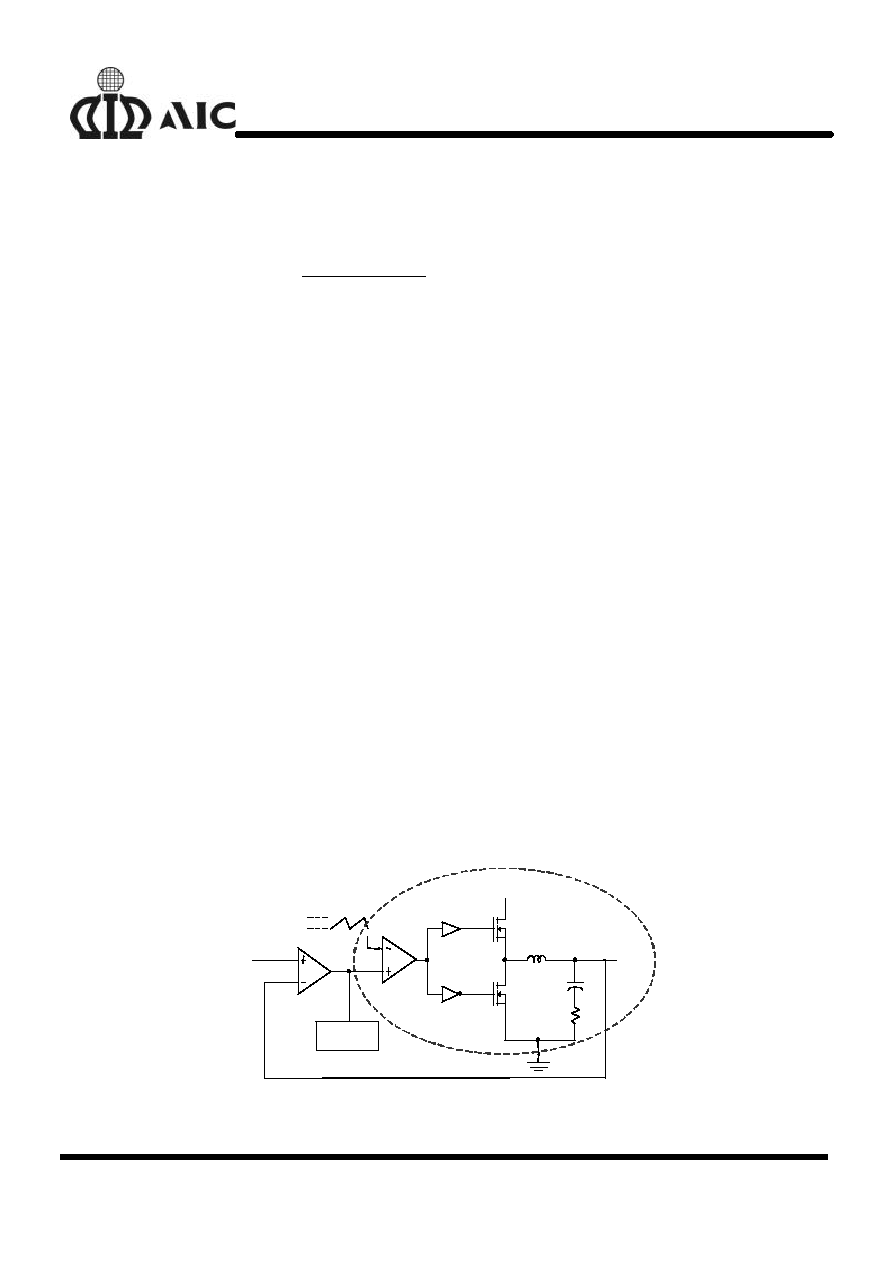
Gate Drive Overlap Protection
The Overlap Protection circuit ensures that the Bot-
tom MOSFET does not turn on until the Upper
MOSFET source has reached a voltage low enough
to ensure that shoot-through will not occur.
Over-Voltage Protection
During operation, a short on the upper PWM
MOSFET (Q1) causes V
OUT1
to increase. When
the output exceed the over-voltage threshold of
116% of DACOUT, the FAULT pin is set to fault
latch and turns Q2 on as required in order to regu-
late VOUT1 to 115% of DACOUT. The fault latch
raises the FAULT/RT pin close to VCC potential.
A separate over-voltage circuit provides protection
during the initial application of power. For voltage on
VCC pin below the power-on reset (and above ~4V),
should VSEN1 exceed 1.0V, the lower MOSFET
(Q2) is driven on as needed to regulate VOUT1 to
1.0V.
Over-Current Protection
All outputs are protected against excessive over-
current. The PWM controller uses upper
MOSFET's on-resistance, R
DS(ON)
to monitor the
current for protection against shorted outputs. All
linear controllers monitor VSEN for under-voltage
events to protect against excessive current.
When the voltage across Q1 (ID
�
R
DS(ON)
) exceeds
the level (200
�
A
�
R
OCSET
), this signal inhibit all
outputs. Discharge soft-start capacitor (Css) with
25
�
A current sink, and increments the counter.
Css recharges and initiates a soft-start cycle again
until the counter increments to 3. This sets the fault
latch to disable all outputs. Fig.
6
illustrates the
over-current protection until an over load on OUT1.
Should excessive current cause VSEN to fall below

AIC1574
14
the linear under-voltage threshold, the LUV signal
sets the over-current latch if C
SS
is fully charged.
Cycling the bias input power (off then on ) reset the
counter and the fault latch.
The over-current function for PWM controller will trip
at a peak inductor current (I
PEAK
) determined by:
I
I
R
R
PEAK
OCSET
OCSET
DS(ON)
=
�
The OC trip point varies with MOSFET's tempera-
ture. To avoid over-current tripping in the normal op-
erating load range, determine the R
OCSET
resistor
from the equation above with:
1. The maximum R
DS(ON)
at the temperature.
2. The minimum I
OCSET
from the specification table.
3. Determine I
PEAK
> I
OUT(MAX)
+ (inductor ripple
current) /2.
PWM OUT1 Voltage Program
The output voltage of the PWM converter is pro-
grammed to discrete levels between 1.3V to 3.5V.
The VID pins program an internal voltage reference
(DACOUT) through a TTL compatible 5 bit digital to
analog converter. The VID pins can be left open for
a logic 1 input, because they are internally pulled
up to 5V by a 70K
resistor. Changing the VID in-
puts during operation is not recommended. All VID
pin combinations resulting in an INHIBIT disable the
IC and the open collector at the PGOOD pin.
OUT2 Voltage Program
The AGP regulator output voltage is internally set to
one of two discrete levels based on the SELECT
pin status. Left SELECT pin open, internal pulled
high, the output voltage is 3.3V. Grounding SE-
LECT pin to GROUND will get the 1.5V output volt-
age.
The status of the SELECT pin can not be changed
during operation of the IC without immediatelly
causing a fault condition.
OUT3 and OUT4 Voltage Program
The GTL bus voltage (1.5V, OUT3) and the chip set
and/or cache memorey voltage (1.8V,OUT4) are in-
ternally set for simpe, low cost implementation ba-
se on the FIX pin left open. Grounding FIX pin al-
lows both output voltages to be set by means of ex-
ternal resistor dividers.
+
AIC1574
FIX
DRV
VSEN
RGND
ROUT
VOUT
3.3V
+
�
=
GND
OUT
OUT
R
R
1
265
.
1
V
V
Adjusting the Output Voltage of OUTPUT 3 and 4
Shutdown
The AIC1574 features a dedicated shetdown pin
(SD). A TTL-compatible logic high signal applied to
this pin shuts down all four outputs and discharge
the soft-start capacitor.
The VID codes resulting in an INHIBIT as shown in
Table 1 also shut down the IC.
n
APPLICATION GUIDE LINES
Layout Considerations
Any inductance in the switched current path gener-
ates a large voltage spike during the switching in-
terval. The voltage spikes can degrade efficiency,

AIC1574
15
radiate noise into the circuit, and lead to device
over-voltage stress. Careful component selection
and tight layout of critical components, and short,
wide metal trace minimize the voltage spike.
A ground plane should be used. Locate the input
capacitors (C
IN
) close to the power switches.
Minimize the loop formed by C
IN
, the upper
MOSFET (Q1) and the lower MOSFET (Q2) as
possible. Connections should be as wide as short
as possible to minimize loop inductance.
The connection between Q1, Q2 and output induc-
tor should be as wide as short as practical. Since
this connection has fast voltage transitions will ea-
sily induce EMI.
The output capacitor (C
OUT
) should be located as
close the load as possible. Because minimize the
transient load magnitude for high slew rate requires
low inductance and resistance in circuit board
The AIC1574 is best placed over a quiet ground
plane area. The GND pin should be connected to
the groundside of the output capacitors. Under no
circumstances should GND be returned to a ground
inside the C
IN
, Q1, Q2 loop. The GND and PGND
pins should be shorted right at the IC. This help to
minimize internal ground disturbances in the IC and
prevents differences in ground potential from dis-
rupting internal circuit operation.
The wiring traces from the control IC to the MOS-
FET gate and source should be sized to carry peak
current.
The Vcc pin should be decoupled directly to GND
by a 2.2
�
F ceramic capacitor, trace lengths should
be as short as possible.

AIC1574
16
Table 1 VOUT1 Voltage Program (0=connected to GND, 1=open or connected to 5V)
For all package versions
PIN NAME
PIN NAME
VID4
VID3
VID2
VID1
VID0
DACOUT
VOLTAGE VID4
VID3
VID2
VID1
VID0
DACOUT
VOLTAGE
0
1
1
1
1
1.30V
1
1
1
1
1
INHIBIT
0
1
1
1
0
1.35V
1
1
1
1
0
2.1 V
0
1
1
0
1
1.40V
1
1
1
0
1
2.2 V
0
1
1
0
0
1.45V
1
1
1
0
0
2.3 V
0
1
0
1
1
1.50V
1
1
0
1
1
2.4 V
0
1
0
1
0
1.55V
1
1
0
1
0
2.5 V
0
1
0
0
1
1.60V
1
1
0
0
1
2.6 V
0
1
0
0
0
1.65V
1
1
0
0
0
2.7 V
0
0
1
1
1
1.70V
1
0
1
1
1
2.8 V
0
0
1
1
0
1.75V
1
0
1
1
0
2.9 V
0
0
1
0
1
1.80 V
1
0
1
0
1
3.0 V
0
0
1
0
0
1.85 V
1
0
1
0
0
3.1 V
0
0
0
1
1
1.90 V
1
0
0
1
1
3.2 V
0
0
0
1
0
1.95 V
1
0
0
1
0
3.3 V
0
0
0
0
1
2.00 V
1
0
0
0
1
3.4 V
0
0
0
0
0
2.05 V
1
0
0
0
0
3.5 V
A multi-layer-printed circuit board is recom-
mended. Figure 11 shows the connections of
the critical components in the converter. The C
IN
and C
OUT
could each represent numerous
physical capacitors. Dedicate one solid layer for
a ground plane and make all critical component
ground connections with vias to this layer.
PWM Output Capacitors
The load transient for the microprocessor core
requires high quality capacitors to supply the
high slew rate (di/dt) current demand.
The ESR (equivalent series resistance) and ESL
(equivalent series inductance) parameters rather
than actual capacitance determine the buck ca-
pacitor values. For a given transient load magni-
tude, the output voltage transient change due to
the output capacitor can be note by the follow-
ing equation:
V
ESR
I
ESL
I
T
OUT
OUT
OUT
=
�
+
�
, where
I
OUT
is transient load current step.
After the initial transient, the ESL dependent
term drops off. Because the strong relationship
between output capacitor ESR and output load
transient, the output capacitor is usually chosen
for ESR, not for capacitance value. A capacitor
with suitable ESR will usually have a larger ca-
pacitance value than is needed for energy stor-
age.
A common way to lower ESR and raise ripple

AIC1574
17
current capability is to parallel several capaci-
tors. In most case, multiple electrolytic capaci-
tors of small case size are better than a single
large case capacitor.
Output Inductor Selection
Inductor value and type should be chosen based
on output slew rate requirement, output ripple
requirement and expected peak current. Induc-
tor value is primarily controlled by the required
current response time. The AIC1570 will provide
either 0% or 100% duty cycle in response to a
load transient. The response time to a transient
is different for the application of load and remove
of load.
t
L
I
V
V
RISE
OUT
IN
OUT
=
�
-
,
t
=
L
I
V
FALL
OUT
OUT
�
.
Where
I
OUT
is transient load current step.
In a typical 5V input, 2V output application, a
3
�
H inductor has a 1A/
�
S rise time, resulting in
a 5
�
S delay in responding to a 5A load current
step. To optimize performance, different combi-
nations of input and output voltage and expected
loads may require different inductor value. A
smaller value of inductor will improve the tran-
sient response at the expense of increase out-
put ripple voltage and inductor core saturation
rating.
Peak current in the inductor will be equal to the
maximum output load current plus half of induc-
tor ripple current. The ripple current is approxi-
mately equal to:
I
=
(V
V
) V
L V
RIPPLE
IN
OUT
OUT
IN
-
�
� �
f
;
f = AIC1574 oscillator frequency.
The inductor must be able to withstand peak
current without saturation, and the copper resis-
tance in the winding should be kept as low as
possible to minimize resistive power loss
Input Capacitor Selection
Most of the input supply current is supplied by
the input bypass capacitor, the resulting RMS
current flow in the input capacitor will heat it up.
Use a mix of input bulk capacitors to control the
voltage overshoot across the upper MOSFET.
The ceramic capacitance for the high frequency
decoupling should be placed very close to the
upper MOSFET to suppress the voltage induced
in the parasitic circuit impedance. The buck ca-
pacitors to supply the RMS current is approxi-
mate equal to:
I
(1 D)
D
I
1
12
V
D
f L
RMS
2
OUT
IN
2
= -
�
�
+
�
�
�
, where
D
V
V
OUT
IN
=
The capacitor voltage rating should be at least
1.25 times greater than the maximum input volt-
age.
PWM MOSFET Selection
In high current PWM application, the MOSFET
power dissipation, package type and heatsink
are the dominant design factors. The conduction
loss is the only component of power dissipation
for the lower MOSFET, since it turns on into
near zero voltage. The upper MOSFET has con-
duction loss and switching loss. The gate char-
ge losses are proportional to the switching fre-
quency and are dissipated by the AIC1574.
However, the gate charge increases the switch-
ing interval, t
SW
, which increase the upper MOS-
FET switching losses. Ensure that both MOS-
FETs are within their maximum junction tem-
AIC1574
18
perature at high ambient temperature by calcu-
lating the temperature rise according to package
thermal resistance specifications.
P
I
R
D
I
V
t
f
2
UPPER
OUT
2
DS(ON)
OUT
IN
SW
=
�
� +
�
�
�
D)
1
(
R
I
P
DS(ON)
2
OUT
LOWER
-
�
�
=
The equations above do not model power loss
due to the reverse recovery of the lower
MOSFET's body diode.
The R
DS(ON)
is different for the two previous
equations even if the type devices is used for
both. This is because the gate drive applied to
the upper MOSFET is different than the lower
MOSFET. Logic level MOSFETs should be se-
lected based on on-resistance considerations,
R
DS(ON)
should be chosen base on input and
output voltage, allowable power dissipation and
maximum required output current. Power dissi-
pation should be calculated based primarily on
required efficiency or allowable thermal dissipa-
tion.
Rectifier Schottky diode is a clamp that prevent
the loss parasitic MOSFET body diode from
conducting during the dead time between the
turn off of the lower MOSFET and the turn on of
the upper MOSFET. The diode's rated reverse
breakdown voltage must be greater than twice
the maximum input voltage.
Linear Controller MOSFET Selection
The power dissipated in a linear regulator is :
)
V
(V
I
P
OUT2
IN2
OUT2
LINEAR
-
�
=
Select a package and heatsink that maintains
junction temperature below the maximum rating
while operation at the highest expected ambient
temperature.
Linear Output Capacitor
The output capacitors for the linear regulator and
linear controller provide dynamic load current.
The linear controller uses dominant pole com-
pensation integrated in the error amplifier and is
insensitive to output capacitor selection. C
OUT2
,
C
OUT3
and C
OUT4
should be selected for tran-
sient load regulation.
PWM Feedback Analysis
+
VDAC
V
OUT
VEA
PWM COMP.
Networks
Compensation
ERROR AMP.
R
ESR
L
O
V
OSC
C
O
Q2
Q1
V
IN
Modulation
Gain

AIC1574
19
The compensation network consists of the error
amplifier and built in compensation networks.
The goal of the compensation network is to
provide for fast response and adequate phase
margin. Phase Margin is the difference between
the closed loop phase at 0dB and 180 degree.
Closed Loop Gain(dB) = Modulation Gain(dB) +
Compensation Gain (dB)
Modulation Gain(dB)
+
+
2
1
log
10
log
20
ESR
OSC
IN
F
F
V
V
�
+
-
-
2
2
2
1
log
10
Q
F
F
F
F
LC
LC
where
O
O
LC
C
L
F
2
1
=
;
O
ESR
ESR
C
R
F
�
�
=
2
1
;
LOAD
O
O
ESR
O
O
R
C
L
R
L
C
Q
1
1
�
+
�
=
The break frequency of Internal Compensation
Gain are given by
KHz
F
Z
6
.
2
1
=
;
KHz
F
Z
24
2
=
;
KHz
F
P
30
1
=
;
KHz
F
P
400
2
=
100
1k
10k
100k
1M
10M
-20
0
20
40
60
F
Frequency (KHz)
F
OdB
20log(V
IN
/
V
OSC
)
F
ESR
F
LC
F
Z1
F
Z2
F
P2
F
P1
Modulation
Gain
Compensation Gain
Closed Loop
Gain
Gain (d
B
)
Bode Plot of Converter Gain
Sampling theory shows that F
0dB
must be less
that half the switching frequency for the loop
stables. But it must be considerably less than
that, or there will be large amplitude switching
frequency ripple at the output. Thus, the usual
practices is to fix F
0dB
at 1/4 to 1/5 the switching
frequency.

AIC1574
20
n
PHYSICAL DIMENSIONS
l
28 LEAD PLASTIC SO (unit: mm)
SYMBOL
MIN
MAX
A
2.35
2.65
A1
0.10
0.30
B
0.33
0.51
C
0.23
0.32
D
17.70
18.10
E
7.40
7.60
e
1.27 (TYP)
H
10.00
10.65
L
0.40
1.27
D
C
L
E
H
e
B
A
A1