HDMP-1637A SerDes
Gigabit Ethernet SerDes Circuit
with Differential PECL Clock
Inputs
CAUTION: As with all semiconductor ICs, it is advised that normal static precautions be taken in handling
and assembly of this component to prevent damage and/or degradation which may be induced by
electrostatic discharge (ESD).
Features
· IEEE 802.3z Gigabit
Ethernet Compatible,
Supports 1250 MBd Gigabit
Ethernet
· Based on X3T11 "10 Bit
Specification"
· Low Power Consumption
· 10 mm 64-pin PQFP Package
· Transmitter and Receiver
Functions Incorporated
onto a Single IC
· 5-Volt Tolerant I/Os
· 10 Bit Wide Parallel TTL
Compatible I/Os
· Single +3.3 V Power Supply
· Differential PECL Clock
Inputs
· 2 kV Human Body ESD
Protection on all Pins
Applications
· 1250 MBd Gigabit
Ethernet Interface
· High Speed Proprietary
Interface
· Backplane Serialization /
Bus Extender
Description
The HDMP-1637A transceiver is a
single silicon bipolar integrated
circuit packaged in a plastic QFP
package. It provides a low-cost,
low-power physical layer solution
for 1250 MBd Gigabit Ethernet or
proprietary link interfaces. It
provides complete Serialize/
Deserialize (SerDes) for copper
transmission, incorporating both
the Gigabit Ethernet transmit and
receive functions into a single
device.
This chip is used to build a high
speed interface (as shown in
Figure 1) while minimizing board
space, power, and cost. It is
compatible with the IEEE 802.3z
specification.
The transmitter section accepts
10-bit wide parallel TTL data and
serializes this data into a high
speed serial data stream. The
parallel data is expected to be
"8B/10B" encoded data, or
equivalent. This parallel data is
latched into the input register of
the transmitter section on the
rising edge of the 125 MHz
reference clock (used as the
transmit byte clock).
The transmitter section's PLL
locks to this user supplied 125
MHz byte clock. This clock is then
multiplied by 10, to generate the
1250 MHz serial signal clock used
to generate the high speed output.
The high speed outputs are
capable of interfacing directly to
copper cables for electrical
transmission or to a separate fiber
optic module for optical
transmission.
The receiver section accepts a
serial electrical data stream at
1250 MBd and recovers the
original 10-bit wide parallel data.
The receiver PLL locks onto the
incoming serial signal and
recovers the high speed serial
clock and data. The serial data is
converted back into 10-bit parallel
data, recognizing the 8B/10B
comma character to establish byte
alignment.
The recovered parallel data is
presented to the user at TTL
compatible outputs. The receiver
section also recovers two 62.5
MHz receiver byte clocks which
are 180 degrees out of phase with
each other. The parallel data is
properly aligned with the rising
edge of alternating clocks.
For test purposes, the transceiver
provides for on-chip local loop-
back functionality controlled
through an external input pin.
Additionally, the byte
synchronization feature may be
disabled. This may be useful in
proprietary applications which use
alternative methods to align the
parallel data.
2
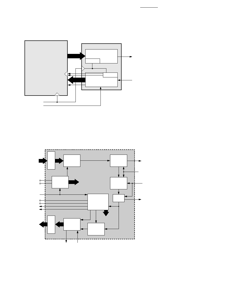
Figure 2. HDMP-1637A Transceiver Block Diagram.
Figure 1. Typical Application using the HDMP-1637A.
HDMP-1637A
PROTOCOL DEVICE
SERIAL DATA OUT
RECEIVER SECTION
PLL
TRANSMITTER SECTION
BYTSYNC
ENBYTSYNC
± REFCLK
SERIAL DATA IN
PLL
RBC0
RBC1
± DOUT
TX
PLL/CLOCK
GENERATOR
± REFCLK
± DIN
RXCAP0
RXCAP1
RBC0
RBC1
BYTSYNC
ENBYTSYNC
OUTPUT
DRIVER
INTERNAL
TX CLOCKS
INPUT
LATCH
DATA BYTE
RX[0-9]
TXCAP1
TXCAP0
DATA BYTE
TX[0-9]
INTERNAL
RX CLOCKS
LOOPEN
INTERNAL
LOOPBACK
OUTPUT
SELECT
FRAME
MUX
RX
PLL/CLOCK
RECOVERY
INPUT
SELECT
FRAME
DEMUX
AND
BYTE SYNC
INPUT
SAMPLER
SIGNAL
DETECT
SIG_DET

3
HDMP-1637A Block
Diagram
The HDMP-1637A was designed
to transmit and receive 10-bit
wide parallel data over a single
high-speed line. The parallel data
applied to the transmitter is
expected to be encoded per the
Gigabit Ethernet specification,
which uses an 8B/10B encoding
scheme with special reserve
characters for link management
purposes. In order to accomplish
this task, the HDMP-1637A
incorporates the following:
· TTL Parallel I/Os
· High Speed Phase Locked
Loops
· Parallel to Serial Converter
· Serial Clock and Data
Recovery
· Comma Character Recognition
· Byte Alignment Circuitry
· Serial to Parallel Converter
INPUT LATCH
The transmitter accepts 10-bit
wide TTL parallel data at inputs
TX[0..9]. The user-provided
reference clock signal, REFCLK,
(from this point forward,
REFCLK is defined as the
difference between PECL inputs
+REFCLK and -REFCLK) is used
as the transmit byte clock. The
TX[0..9] and REFCLK signals
must be properly aligned, as
shown in Figure 3.
TX PLL/CLOCK GENERATOR
The transmitter Phase Locked
Loop and Clock Generator (TX
PLL/CLOCK GENERATOR) block
is responsible for generating all
internal clocks needed by the
transmitter section to perform its
functions. These clocks are based
on the supplied reference byte
+/- DIN. When LOOPEN is set
high, the high speed serial signal
is internally looped-back from the
transmitter section to the receiver
section. This feature allows for
loop back testing exclusive of the
transmission medium.
RX PLL/CLOCK RECOVERY
The RX PLL/CLOCK RECOVERY
block is responsible for frequency
and phase locking onto the
incoming serial data stream and
recovering the bit and byte
clocks. An automatic locking
feature allows the Rx PLL to lock
onto the input data stream
without external PLL training
controls. It does this by
continually frequency locking
onto the 125 MHz reference
clock, and then phase locking
onto the input data stream. An
internal signal detection circuit
monitors the presence of the
input, and invokes the phase
detection as the data stream
appears. Once bit locked, the
receiver generates the high speed
sampling clock at 1250 MHz for
the input sampler, and recovers
the two 62.5 MHz receiver byte
clocks (RBC1/RBC0). These
clocks are 180 degrees out of
phase with each other, and are
alternately used to clock the 10-
bit parallel output data.
INPUT SAMPLER
The INPUT SAMPLER is
responsible for converting the
serial input signal into a retimed
serial bit stream. In order to
accomplish this, it uses the high
speed serial clock recovered from
the RX PLL/CLOCK RECOVERY
block. This serial bit stream is
sent to the FRAME DEMUX and
BYTE SYNC block.
clock (REFCLK). REFCLK is
used as both the frequency
reference clock for the PLL and
the transmit byte clock for the
incoming data latches. It is
expected to be 125 MHz and
properly aligned to the incoming
parallel data (see Figure 3). This
clock is then multiplied by 10 to
generate the 1250 MHz clock
necessary for clocking the high
speed serial outputs.
FRAME MUX
The FRAME MUX accepts the 10-
bit wide parallel data from the
INPUT LATCH. Using internally
generated high speed clocks, this
parallel data is multiplexed into
the 1250 MBd serial data stream.
The data bits are transmitted
sequentially, from the least
significant bit (TX[0]) to the
most significant bit (TX[9]).
OUTPUT SELECT
The OUTPUT SELECT block
provides for an optional internal
loopback of the high speed serial
signal for testing purposes.
In normal operation, LOOPEN is
set low and the serial data stream
is placed at +/- DOUT. When
wrap-mode is activated by setting
LOOPEN high, the +/- DOUT
pins are held static at logic 1 and
the serial output signal is
internally wrapped to the INPUT
SELECT box of the receiver
section.
INPUT SELECT
The INPUT SELECT block
determines whether the signal at
+/- DIN or the internal loop-back
serial signal is used. In normal
operation, LOOPEN is set low
and the serial data is accepted at

4
FRAME DEMUX AND BYTE
SYNC
The FRAME DEMUX AND BYTE
SYNC block is responsible for
restoring the 10-bit parallel data
from the high speed serial bit
stream. This block is also
responsible for recognizing the
comma character (or a K28.5
character) of positive disparity
(0011111xxx). When
recognized, the FRAME DEMUX
AND BYTE SYNC block works
with the RX PLL/CLOCK
RECOVERY block to properly
align the receive byte clocks to
the parallel data. When a comma
character is detected and
realignment of the receiver byte
clocks (RBC1/RBC0) is
necessary, these clocks are
stretched, not slivered, to the
next possible correct alignment
position. These clocks will be
fully aligned by the start of the
second 2-byte ordered set. The
second comma character
received shall be aligned with the
rising edge of RBC1. As per the
8B/10B encoding scheme,
comma characters must not be
transmitted in consecutive bytes
to allow the receiver byte clocks
to maintain their proper
recovered frequencies.
OUTPUT DRIVERS
The OUTPUT DRIVERS present
the 10-bit parallel recovered data
byte properly aligned to the
receive byte clocks (RBC1/
RBC0), as shown in Figure 5.
These output data buffers
provide TTL compatible signals.
SIGNAL DETECT
The SIGNAL DETECT block
examines the differential
amplitude of the inputs
±
DIN.
When this input signal is too
small, it outputs a logic 0 at
SIG_DET (refer to SIG_DET pin
definition for detection
thresholds), and at the same
time, forces the parallel output
RX[0]..RX[9] to all logic one
(1111111111). The main
purpose of this circuit is to
prevent the generation of random
data when the serial input lines
are disconnected. When the
signal at
±
DIN is of a valid
amplitude, SIG_DET is set to
logic 1, and the output of the
INPUT SELECT block is passed
through.

5
Figure 4. Transmitter Latency.
Figure 3. Transmitter Section Timing.
HDMP-1637A (Transmitter Section)
Timing Characteristics
T
A
= 0
°
C to +70
°
C, V
CC
= 3.15 V to 3.45 V
Symbol
Parameter
Units
Min.
Typ.
Max.
t
setup
Setup Time
nsec
1.5
t
hold
Hold Time
nsec
1.0
t_txlat
[1]
Transmitter Latency
nsec
3.5
bits
4.4
Note:
1. The transmitter latency, as shown in Figure 4, is defined as the time between the latching in of the parallel data word (as triggered
by the rising edge of the transmit byte clock, REFCLK) and the transmission of the first serial bit of that parallel word (defined by
the rising edge of the first bit transmitted).
DATA
DATA
TX[9]-TX[0]
tSETUP
tHOLD
REFCLK
DATA
DATA
DATA
0.0 V AC
2.0 V
0.8 V
DATA BYTE B
DATA BYTE C
TX[0]-TX[9]
DATA BYTE A
± DOUT
0.0 V AC
DATA BYTE B
t_TXLAT
T5
T6
T7
T8
T9
T0
T1
T2
T3
T4
T5
T6
T7
T8
T9
T0
T1
T2
T3
T4
T5
REFCLK