
Preliminary Data Sheet
August 2001
TAAD08JU2 Newport
T1/E1/J1/J2 ATM Processor
1 Features
s
System-on-a-chip integrated circuit supports low-
speed ATM access for next-generation wireless
base transmission station (BTS), base station con-
troller BSC), and remote access concentrator
(RAC) applications.
s
IC provides an integrated octal framer that sup-
ports T1/E1/J1/J2 formats.
s
Supports inverse multiplexing for ATM (IMA) over
selected group and link mappings ranging from
four two-link groups up to one eight-link group per
ATM Forum AF-PHY-0086.001.
s
Integrates an ATM adaptation layer 2 (AAL2) seg-
mentation and reassembly (SAR) function for sup-
port of low-speed data or voice traffic per ITU
I.363.2.
s
Provides AAL5 SAR functionality per ITU I.363.5.
s
Provides quality of service (QoS) connection iden-
tifier (CID) multiplexing per ITU I.366.1.
s
Enables ATM layer user network interface (UNI) or
IMA mode, selectable on a per-link basis for flexi-
ble transport of delay critical voice and data traffic.
s
Guarantees QoS for a variety of traffic types
(including delay-sensitive voice, real-time data,
non-real-time data, and signaling information)
through an advanced hierarchical three-level prior-
ity scheduler and per-VC queueing.
s
Supports 2047 AAL2 CIDs.
s
Supports 2048 high-speed data connections or vir-
tual circuits (VCs) via embedded context memory;
filters control cells and accepts control cells via a
host microprocessor interface.
s
Software package includes the following:
-- Software device manager source code (C-
based device manager ready-to-use with host
RTOS) and firmware for embedded controller
(executable binary).
-- User manual available for device manager soft-
ware.
s
Designed in 0.16 Ąm, low-power CMOS technol-
ogy.
2 Physical
s
3.3 V digital I/O compatibility; 1.5 V core power
s
520 enhanced ball-grid array (EBGA) package
s
Ł40
o
C to +85
o
C temperature range
3 Standards
ITU I.363.2
ITU I.366.1
ITU I.363.5
ITU I.432
ITU I.361
ITU I.371
ITU G.703
ITU G.704
ITU G.804
ITU G.732
ITU G.706
ITU I.610
ITU G.775
ITU G.733
ITU G.735
ITU G.965
ITU O.162
ANSI* T1.403
ANSI T1.231
ATM Forum af-phy-0086.001
ATM Forum af-phy-0029.000
ATM Forum af-phy-0039.000
ATM Forum Traffic Management 4.1
ETS 300.417-1-1
TR-NWT-000170
* ANSI is a registered trademark of American National Standards
Institute, Inc.

Table of Contents
2
Agere Systems Inc.
Preliminary Data Sheet
August 2001
T1/E1/J1/J2 ATM Processor
TAAD08JU2 Newport
Contents
Page
1
Features...........................................................................................................................................................1
2
Physical ...........................................................................................................................................................1
3
Standards ........................................................................................................................................................1
4
Description.....................................................................................................................................................16
5
Pin Definitions................................................................................................................................................17
6
Pin Description...............................................................................................................................................17
7
Package Pin Layout.......................................................................................................................................25
8
Block Diagram ...............................................................................................................................................31
9
Functional Overview ......................................................................................................................................32
9.1
Receive Direction Data Flow................................................................................................................32
9.1.1
PHY Layer...............................................................................................................................32
9.1.2
Low-Speed PHY Links ............................................................................................................32
9.1.3
Medium-Speed PHY Links ......................................................................................................33
9.1.4
High-Speed PHY Links ...........................................................................................................33
9.1.5
TC and IMA Layers .................................................................................................................33
9.1.6
ATM Layer...............................................................................................................................34
9.1.7
AAL Engine .............................................................................................................................34
9.1.8
Embedded Device Controller ..................................................................................................35
9.2
Transmit Direction Data Flow...............................................................................................................35
9.2.1
SSCS/AAL Layer Interaction...................................................................................................35
9.2.2
ATM Layer...............................................................................................................................35
9.2.3
IMA/TC Layer ..........................................................................................................................36
9.2.4
PHY Layer...............................................................................................................................36
10 Modes of Operation .......................................................................................................................................37
10.1 Interface Modes ...................................................................................................................................37
10.1.1 UTOPIA-2 Expansion Port Multiplexing Modes ......................................................................37
10.1.2 System Interface Port Multiplexing Modes..............................................................................38
10.1.3 Line Interface Modes...............................................................................................................38
10.2 Device Operating Modes......................................................................................................................38
10.2.1 Operating Mode 1: Internal Framer Mode...............................................................................39
10.2.2 Operating Mode 2: External PHY/TC Mode ............................................................................41
10.2.3 Operating Mode 3: SAR Slave Mode ......................................................................................42
10.2.4 Operating Mode Summary ......................................................................................................42
11 Applications ...................................................................................................................................................43
11.1 BTS Network Interface Termination .....................................................................................................43
11.2 VToA Trunking Application...................................................................................................................46
11.3 Low-Speed ATM Access......................................................................................................................47
11.4 AAL2 Crossconnect .............................................................................................................................47
12 Submodule Functional Description ................................................................................................................48
12.1 Embedded Device Controller (EDC) ....................................................................................................48
12.1.1 Introduction .............................................................................................................................48
12.1.2 Features ..................................................................................................................................48
12.1.3 EDC Functional Description ....................................................................................................48
12.1.4 Host Interface..........................................................................................................................48
12.1.5 Host Interface Signals and Timing ..........................................................................................49
12.1.6 Host Interactions .....................................................................................................................50
13 Framer Block .................................................................................................................................................53
13.1 Introduction ..........................................................................................................................................53
13.2 Features ...............................................................................................................................................53
13.3 Framer-to-Line Interface Unit Physical Interface..................................................................................54
13.3.1 Clocking Modes.......................................................................................................................54

Table of Contents
(continued)
Contents
Page
Preliminary Data Sheet
TAAD08JU2 Newport
August 2001
T1/E1/J1/J2 ATM Processor
Agere Systems Inc.
Lucent Technologies--Proprietary
3
Use pursuant to Company instructions
13.4 Frame Formats.....................................................................................................................................55
13.5 Transmit Framer Functions ..................................................................................................................56
13.6 DS1 Transparent Framing Format .......................................................................................................56
13.7 CEPT 2.048 Basic Frame Structure Transparent Framing Format......................................................57
13.8 Receive Framer Nonalignment Mode (DS1/E1)...................................................................................58
13.9 Loss of Frame Alignment Criteria.........................................................................................................58
13.9.1 Frame Bit Errors......................................................................................................................58
13.9.2 CRC Errors..............................................................................................................................58
13.10 Frame Alignment Criteria .....................................................................................................................58
13.11 Performance Monitoring Functional Integration Into Framer................................................................59
13.12 Performance Report Message .............................................................................................................62
13.13 ESF Data Link ......................................................................................................................................64
13.14 Facility Data Link..................................................................................................................................64
13.15 Receive Data Link Functional Description ...........................................................................................64
13.16 SLC-96 Superframe Receive Data Link ...............................................................................................65
13.17 DDS Receive Data Link Stack .............................................................................................................65
13.18 CEPT; CEPT CRC-4 (100 ms); CEPT CRC-4 (400 ms) Multiframe Sa Bits Receive Stack................65
13.19 Receive Data Link Stack Idle Modes ...................................................................................................65
13.20 Transmit Facility Data Link Functional Description ..............................................................................66
13.21 SLC-96 Superframe Transmit Data Link ..............................................................................................66
13.22 DDS Transmit Data Link Stack ............................................................................................................66
13.23 Transmit ESF Data Link Bit-Oriented Messages .................................................................................66
13.24 CEPT, CEPT Multiframe Transmit Data Link Sa Bits Stack.................................................................67
13.25 Transmit Data Link Stack Idle Modes ..................................................................................................68
13.26 SLC-96, DDS, or CEPT ESF Frame Alignment ...................................................................................68
13.27 Concentration Highway Interface (CHI) ...............................................................................................68
13.28 Transmit/Receive System Interface Features ......................................................................................68
13.29 Double NOTFAS System Time-Slot Mode...........................................................................................69
13.30 Transparent Mode................................................................................................................................69
13.31 Loopbacks............................................................................................................................................69
13.32 Nominal CHI Timing .............................................................................................................................70
13.33 CHI Timing with CHI Double Time-Slot Timing (CHIDTS) Mode Enabled ...........................................71
13.34 Clocking Scheme .................................................................................................................................71
14 Transmission Convergence (TC) Block .........................................................................................................72
14.1 Introduction ..........................................................................................................................................72
14.2 Features ...............................................................................................................................................72
14.3 TC--Receive Direction.........................................................................................................................73
14.4 TC--Transmit Direction........................................................................................................................73
14.4.1 HEC Generation/Checking......................................................................................................74
14.5 Cell Delineation ....................................................................................................................................74
14.6 Cell Payload Scrambling/Descrambling ...............................................................................................74
14.7 Cell Mapping ........................................................................................................................................74
14.8 Facility Maintenance ............................................................................................................................74
14.9 Cell Rate Decoupling ...........................................................................................................................74
14.10 Functionality .........................................................................................................................................75
15 Inverse Multiplexing for ATM (IMA) Block......................................................................................................76
15.1 Introduction ..........................................................................................................................................76
15.2 Features ...............................................................................................................................................77
15.3 Multi-PHY UTOPIA Slave Interface......................................................................................................78
15.4 Link Processor .....................................................................................................................................78
15.5 Group Processor ..................................................................................................................................79
15.6 Delay Compensation Buffer (DCB) ......................................................................................................80

Table of Contents
(continued)
Contents
Page
Preliminary Data Sheet
TAAD08JU2 Newport
August 2001
T1/E1/J1/J2 ATM Processor
4
Lucent Technologies--Proprietary
Agere Systems Inc.
Use pursuant to Company instructions
15.7 Programming the DCB .........................................................................................................................87
15.7.1 Link Startup Guardband Field .................................................................................................87
15.7.2 Link Maximum Operational Delay ...........................................................................................87
15.8 Features Not Supported in IMA............................................................................................................87
16 ATM Port Controller (APC) Block ..................................................................................................................89
16.1 Introduction ..........................................................................................................................................89
16.2 Architecture ..........................................................................................................................................90
16.3 Features ...............................................................................................................................................91
16.4 Summary of Commands ......................................................................................................................92
16.5 Buffer Management..............................................................................................................................92
16.6 Scheduling ...........................................................................................................................................94
16.6.1 Ingress Scheduling..................................................................................................................94
16.6.2 Fabric Backpressure ...............................................................................................................95
16.6.3 Egress Scheduling ..................................................................................................................95
16.7 ABR Flow Control.................................................................................................................................95
16.8 Control Plane Functions.......................................................................................................................96
16.8.1 APC Support for Control Plane Functions...............................................................................96
16.9 Management Plane Functions .............................................................................................................96
16.9.1 Operation Administration and Maintenance (OAM) ................................................................96
16.10 Statistics Counters ...............................................................................................................................97
16.11 Ingress Enqueue Operations ...............................................................................................................97
16.11.1 Connection Look Up................................................................................................................98
16.11.2 OAM Processing .....................................................................................................................99
16.11.3 Policing....................................................................................................................................99
16.11.4 Buffer Thresholding...............................................................................................................100
16.11.5 Egress--APC VC Queueing Structure..................................................................................100
16.12 Connection Management ...................................................................................................................100
16.12.1 Connection Admission Control..............................................................................................100
16.12.1.1 CBR ......................................................................................................................100
16.12.1.2 rt-VBR ...................................................................................................................101
16.12.1.3 nrt-VBR .................................................................................................................101
16.12.1.4 ABR.......................................................................................................................101
16.12.1.5 UBR ......................................................................................................................101
17 ATM Adaption Layer (AAL) Block ................................................................................................................102
17.1 Introduction ........................................................................................................................................102
17.2 Features .............................................................................................................................................102
17.3 Definitions ..........................................................................................................................................104
17.4 Architecture ........................................................................................................................................105
17.4.1 Datapath Flows .....................................................................................................................105
17.4.2 Subblock Architecture ...........................................................................................................107
17.4.3 Subblock Definition ...............................................................................................................109
17.4.4 Subblock Flows .....................................................................................................................109
17.4.5 Address Translation ..............................................................................................................110
17.4.6 Queueing and Scheduling.....................................................................................................111
17.4.7 Modes ...................................................................................................................................111
17.4.8 User Data Types (UDT) and AAL Types...............................................................................111
17.4.9 UDT: ATM Cell ......................................................................................................................113
17.4.10 AAL Type: AAL0....................................................................................................................113
17.4.11 AAL Type: AAL2....................................................................................................................113
17.4.12 AAL2 Subtype: SPAAL2 (Single-Packet AAL2) ....................................................................114
17.4.13 CPS-AAL0.............................................................................................................................114
17.4.14 AAL Type: AAL5....................................................................................................................115

Table of Contents
(continued)
Contents
Page
Preliminary Data Sheet
TAAD08JU2 Newport
August 2001
T1/E1/J1/J2 ATM Processor
Agere Systems Inc.
Lucent Technologies--Proprietary
5
Use pursuant to Company instructions
17.4.15 UDT: Packet ATM (PATM)....................................................................................................115
17.4.16 UDT: HPF..............................................................................................................................116
17.4.17 AAL Type: NPAAL (No Particular AAL).................................................................................118
17.4.18 Nonuser Data Types: ESI Messages ....................................................................................118
17.4.18.1 ESI Message Format ............................................................................................118
17.4.18.2 ESI Violation Code................................................................................................119
17.4.18.3 ESI Packet Length ................................................................................................119
17.4.19 Service Types .......................................................................................................................119
17.4.20 CPS_SERVICE .....................................................................................................................120
17.4.21 SEG_AAL2_SSSAR_SERVICE............................................................................................121
17.4.22 SEG_AAL2_SSTED_SERVICE ............................................................................................121
17.4.23 SEG_AAL5_SERVICE ..........................................................................................................122
17.4.24 TRANSPARENT_SERVICE..................................................................................................122
17.4.25 REASS_AAL2_SSSAR_SERVICE .......................................................................................122
17.4.26 REASS_AAL2_SSTED_SERVICE .......................................................................................122
17.4.27 REASS_AAL5_SERVICE .....................................................................................................123
17.5 Provisioning........................................................................................................................................124
17.5.1 Some Notes on Terminology and Command Referencing....................................................124
17.5.2 System Interface ...................................................................................................................124
17.5.3 Port Table..............................................................................................................................125
17.5.4 MEMI Shared Memory ..........................................................................................................126
17.5.4.1 MEMI-SM Provisioning Constraints ......................................................................126
17.5.4.2 VC Table ...............................................................................................................127
17.5.4.3 AAL2 VC Table .....................................................................................................128
17.5.4.4 Connection Table..................................................................................................129
17.5.4.5 Level 0 Queue Descriptor .....................................................................................130
17.5.4.6 ICID Table.............................................................................................................131
17.5.5 SQASE Shared Memory .......................................................................................................131
17.6 Configuration......................................................................................................................................132
17.6.1 Connection and Channel Setup ............................................................................................132
17.6.1.1 AAL2 Data Flow (CPS/SSSAR/SSTED) ...............................................................134
17.6.1.2 CPS-AAL0 Data Flow ...........................................................................................135
17.6.1.3 AAL0/AAL5 Data Flow ..........................................................................................135
17.6.1.4 HPF Data Flow......................................................................................................135
17.6.2 Configuration for QoS ...........................................................................................................136
17.6.2.1 Packet Scheduling ................................................................................................136
17.6.2.2 IL1Q Scheduler Algorithm.....................................................................................136
17.6.3 Configuration for QoS ...........................................................................................................137
17.6.3.1 IL2Q Scheduler Algorithm.....................................................................................137
17.6.3.2 Latency Policing....................................................................................................137
17.6.3.3 Latency Sensitive Data Discard ............................................................................138
17.6.3.4 Internal Queue Housekeeping ..............................................................................138
17.6.3.5 Reference Clock Generation.................................................................................138
17.6.3.6 Latency Timer Enable/Disable Functions .............................................................139
17.6.3.7 Queue Length Policing..........................................................................................139
17.6.3.8 Connection Queue Length Policing ......................................................................139
17.6.3.9 Intra-Level 1 Queue and Level 1 Queue Length Policing .....................................140
17.6.3.10 Intra-Level 2 Queue Length Policing.....................................................................141
17.6.4 Configuration for Exceptions .................................................................................................142
17.7 Interface Timing Diagrams .................................................................................................................145
17.7.1 SIF UT2/UT2+ Interface ........................................................................................................145
17.7.2 Polling Algorithms For UTOPIA 2 and UT2+ Modes .............................................................153

Table of Contents
(continued)
Contents
Page
Preliminary Data Sheet
TAAD08JU2 Newport
August 2001
T1/E1/J1/J2 ATM Processor
6
Lucent Technologies--Proprietary
Agere Systems Inc.
Use pursuant to Company instructions
17.7.2.1 Receive Interface Polling ......................................................................................153
17.7.2.2 Transmit Interface Polling .....................................................................................154
17.7.3 NIF ........................................................................................................................................155
17.7.4 ESI ........................................................................................................................................155
18 Firmware Flows ...........................................................................................................................................156
18.1 Software Architecture Overview.........................................................................................................156
18.2 Provisioning........................................................................................................................................157
18.2.1 PHY Layer Provisioning ........................................................................................................157
18.2.2 Link Provisioning ...................................................................................................................159
18.2.3 Connection Provisioning .......................................................................................................161
18.2.4 AAL2 Provisioning.................................................................................................................161
18.2.5 System Interface Provisioning...............................................................................................161
18.3 Operation ...........................................................................................................................................161
18.3.1 Management Plane Interaction via External Host .................................................................163
18.3.2 Provisioning of AAL2 Connection..........................................................................................163
18.4 Alarm Generation and Reporting .......................................................................................................164
18.4.1 Layer 1 (PHY) .......................................................................................................................166
18.4.2 ATMF Specifications .............................................................................................................166
18.4.3 E1/ATMF ...............................................................................................................................167
18.4.4 Layer 2 (TC) ..........................................................................................................................167
18.4.5 Layer 3 (ATM) .......................................................................................................................168
18.4.6 Layer 4 (AAL) ........................................................................................................................168
19 Embedded Device Controller (EDC) Firmware............................................................................................169
19.1 Firmware Architecture ........................................................................................................................170
19.2 Reset and Booting..............................................................................................................................171
19.3 Initialization ........................................................................................................................................171
20 Commands and Indications .........................................................................................................................172
21 Commands ..................................................................................................................................................172
21.1 Command Register Structure.............................................................................................................172
21.1.1 Command Sequences...........................................................................................................175
21.2 Global Commands .............................................................................................................................176
21.2.1 NPT_CMD_ECHO Command...............................................................................................176
21.2.2 NPT_ENABLE_PROCESSING Command ...........................................................................176
21.2.3 NPT_GLBCLK_RATE Command..........................................................................................176
21.3 PHY Layer Commands ......................................................................................................................176
21.3.1 NPT_PHY_CONFIG_GLOBALS Command .........................................................................177
21.3.2 NPT_PHY_CONFIG_LINK Command ..................................................................................184
21.3.3 NPT_PHY_ADD_LINK Command ........................................................................................191
21.3.4 NPT_PHY_DELETE_LINK Command ..................................................................................192
21.3.5 NPT_PHY_FRAMER__TEST_LINK Command....................................................................193
21.3.6 NPT_PHY_SEND_ALARMS Command ...............................................................................194
21.3.7 NPT_PHY_FRAMER_LOOPBACK Command .....................................................................194
21.3.8 NPT_PHY_CHI_LOOPBACK Command ..............................................................................195
21.3.9 NPT_PHY_IMA_CONFIG_GROUP Command ....................................................................196
21.3.10 NPT_PHY_IMA_DELETE_GROUP Command ....................................................................198
21.3.11 NPT_PHY_IMA_INHIBIT_LINK Command...........................................................................198
21.3.12 NPT_PHY_IMA_INHIBIT_GROUP Command......................................................................198
21.3.13 NPT_PHY_IMA_TEST_LINK Command ..............................................................................198
21.3.14 NPT_PHY_SET_STATS Command .....................................................................................199
21.3.15 NPT_PHY_SINGLE_STATS Command ...............................................................................199
21.3.16 NPT_PHY_GET_STATE.......................................................................................................199
21.3.17 NPT_PHY_READ_REG........................................................................................................200

Table of Contents
(continued)
Contents
Page
Preliminary Data Sheet
TAAD08JU2 Newport
August 2001
T1/E1/J1/J2 ATM Processor
Agere Systems Inc.
Lucent Technologies--Proprietary
7
Use pursuant to Company instructions
21.3.18 NPT_PHY_SET_LINK_ALARMS Command ........................................................................200
21.3.19 NPT_PHY_SET_GROUP_ALARMS Command ...................................................................202
21.3.20 NPT_PHY_FRAMER_BOM Command.................................................................................203
21.3.21 NPT_PHY_FRAMER_DL_THRESHOLDS Command..........................................................203
21.3.22 NPT_PHY_FRAMER_AUTOPRM Command.......................................................................204
21.3.23 NPT_PHY_FRAMER_DATA_LINK_MSG Command ...........................................................205
21.3.24 NPT_PHY_FRAMER_FDL_STACK Command ....................................................................205
21.4 ATM Layer Commands ......................................................................................................................207
21.4.1 APC Modes ...........................................................................................................................207
21.4.2 ATM Connection Tags ..........................................................................................................207
21.4.3 Calculation of Connection Buffer and Bandwidth Parameters ..............................................207
21.4.4 ATM Scheduling....................................................................................................................209
21.4.5 ATM-Layer OAM ...................................................................................................................212
21.4.6 APC Connection Defect States .............................................................................................215
21.4.7 NPT_ATM_INIT Command ...................................................................................................215
21.4.8 NPT_ATM_SCHED_INIT# Commands.................................................................................221
21.4.9 NPT_ATM_SCHED_CONFIG Command .............................................................................222
21.4.10 NPT_ATM_SET_ALARM_MASK Command ........................................................................224
21.4.11 NPT_ATM_SET_STATS_MASK Command .........................................................................224
21.4.12 NPT_ATM_ADD_CONN Command......................................................................................232
21.4.13 NPT_ATM_DELETE_UNI_CONN Command .......................................................................238
21.4.14 NPT_ATM_DELETE_BI_CONN Command..........................................................................239
21.4.15 NPT_ATM_SET_CONN_STATS Command.........................................................................241
21.4.16 NPT_ATM_SET_CONN_FAULT_STATE Command ...........................................................241
21.4.17 NPT_ATM_SET_CONN_OAM_CC Command.....................................................................242
21.4.18 NPT_ATM_ENABLE_CONN_OAM_PM Command .............................................................243
21.4.19 NPT_ATM_DISABLE_CONN_OAM_PM Command ............................................................243
21.4.20 NPT_ATM_INSERT_CELLS Command ...............................................................................244
21.4.21 NPT_ATM_GET_STATS Command.....................................................................................245
21.4.22 NPT_ATM_READ_APC Command ......................................................................................245
21.4.23 NPT_ATM_READ_DRAM Command ...................................................................................246
21.5 ATM Adaptation Layer Commands ....................................................................................................248
21.5.1 NPT_AAL_ADAPBLK_MEM_ALLC Command.....................................................................249
21.5.1.1 VC Table ...............................................................................................................249
21.5.1.2 AAL2 VC Table .....................................................................................................249
21.5.1.3 Connection Table..................................................................................................249
21.5.1.4 Level 0 Descriptors ...............................................................................................249
21.5.2 NPT_AAL_FREE_LIST_ALLC Command ............................................................................250
21.5.3 NPT_AAL_NIF_FREE_LIST_ALLC Command.....................................................................250
21.5.4 NPT_AAL_SIF_TRANSMIT_CONFIG Command.................................................................251
21.5.5 NPT_AAL_SIF_RECEIVE_CONFIG Command ...................................................................252
21.5.6 NPT_AAL_SIF_RECEIVE_PORT_CONTROL Command....................................................252
21.5.7 NPT_AAL_NIF_TRANSMIT_CONFIG Command ................................................................252
21.5.8 NPT_AAL_NIF_TRANSMIT_PORT_CONTROL Command.................................................253
21.5.9 NPT_AAL_NIF_RECEIVE_CONFIG Command ...................................................................254
21.5.10 NPT_AAL_SERVICE_COUNT Command ............................................................................254
21.5.11 NPT_AAL_CONN_QUE_LEN_POL Command ....................................................................254
21.5.12 NPT_AAL_QUE_LEN_POL_TAB Command........................................................................255
21.5.13 NPT_AAL_IL2_QUE_SHARE Command .............................................................................255
21.5.14 NPT_AAL_IL2_QUE_PRIVATE Command ..........................................................................256
21.5.15 NPT_AAL_L1_QUE_QOS Command...................................................................................257
21.5.16 NPT_AAL_IL1_QUE_POL_SCHED Command ....................................................................258

Table of Contents
(continued)
Contents
Page
Preliminary Data Sheet
TAAD08JU2 Newport
August 2001
T1/E1/J1/J2 ATM Processor
8
Lucent Technologies--Proprietary
Agere Systems Inc.
Use pursuant to Company instructions
21.5.17 NPT_AAL_IDU_SDU_TABLE Command .............................................................................258
21.5.18 NPT_AAL_ADD_CONN Command ......................................................................................259
21.5.19 NPT_AAL_ADD_CHANNEL Command................................................................................262
21.5.20 NPT_AAL_RAS_TIMER Command ......................................................................................264
21.5.21 NPT_AAL_ENABLE Command ............................................................................................264
21.5.22 NPT_ AAL_DELETE_CHANNEL Command ........................................................................265
21.5.23 NPT_ AAL_DELETE_CONN Command ...............................................................................265
21.5.24 NPT_AAL_SET_STAT_MODE Command............................................................................267
21.5.25 NPT_AAL_SET_CONNCHAN_STATS Command ...............................................................267
21.5.26 NPT_AAL_ADD_STAT Command........................................................................................267
21.5.27 Block Exception Code ...........................................................................................................269
21.5.28 NPT_AAL_FREE_STAT Command......................................................................................271
21.5.29 NPT_AAL_GET_STAT Command ........................................................................................271
21.5.30 NPT_AAL_REPORT_ALL_STATS Command......................................................................272
21.5.31 NPT_AAL_INSERT_ALARMS Command.............................................................................272
21.5.32 NPT_AAL_INSERT_PACKETS Command...........................................................................273
22 Indications....................................................................................................................................................274
22.1 Indication Register Structure..............................................................................................................274
22.2 Indications of the Command-Complete Type.....................................................................................275
22.2.1 Global Command-Complete Indications ...............................................................................276
22.2.1.1 NPT_GLB_CLK_RATE_ERR Indication ...............................................................276
22.2.2 PHY Layer Command-Complete Indications ........................................................................276
22.2.3 ATM-Layer Command-Complete Indications ........................................................................283
22.3 Indications of the Data Type ..............................................................................................................290
22.3.1 Data Indications from the PHY Layer....................................................................................290
22.3.1.1 NPT_PHY_BOM_RCVD Indication.......................................................................290
22.3.1.2 NPT_PHY_BOM_SENT Indication .......................................................................291
22.3.1.3 NPT_PHY_FRAMER_DATA_LINK_RCVD Indication ..........................................291
22.3.1.4 NPT_PHY_FRAMER_DATA_LINK_SENT Indication...........................................292
22.3.1.5 NPT_PHY_FRAMER_FDL_STACK_RCVD Indication.........................................293
22.3.1.6 NPT_PHY_FRAMER_FDL_STACK_SENT Indication .........................................293
22.3.2 Data Indications from the ATM Layer....................................................................................293
22.3.2.1 NPT_ATM_DATA Indication .................................................................................296
22.3.3 Data Indications from the ATM Adaption Layer ....................................................................296
22.4 Indications of the Statistics Type........................................................................................................297
22.4.1 Statistics Indications from the PHY Layer .............................................................................297
22.4.2 Statistics Indications from the ATM Layer: Per-Connection Statistics ..................................301
22.4.2.1 NPT_ATM_CONN_STATS Indication...................................................................301
22.4.3 Statistics Indications from the ATM Layer: Global Statistics .................................................301
22.4.4 Statistics Indications from AAL Layer....................................................................................302
22.4.4.1 NPT_AAL_FLOW_STATS Indication....................................................................303
22.4.4.2 NPT_AAL_AAL2VC_STATS Indication ................................................................303
22.4.4.3 NPT_AAL_PROG_STATS Indication ...................................................................304
22.4.5 Indications of the Global Alarm Type ....................................................................................304
22.4.6 Alarm Indication from the Global Layer.................................................................................304
22.4.6.1 NPT_GLB_RDY Indication....................................................................................305
22.4.6.2 NPT_POLLING_TIMER Indication........................................................................305
22.4.7 Indications of the Alarm Type, Excluding Global Alarms ......................................................306
22.4.8 Alarm Indications from the PHY Layer ..................................................................................306
22.4.9 PHY Link Alarms ...................................................................................................................306
22.4.9.1 NPY_PHY_IMA_GROUP_ALARMS.....................................................................310
22.4.10 Alarm Indications from the AAL Layer...................................................................................310

Table of Contents
(continued)
Contents
Page
Preliminary Data Sheet
TAAD08JU2 Newport
August 2001
T1/E1/J1/J2 ATM Processor
Agere Systems Inc.
Lucent Technologies--Proprietary
9
Use pursuant to Company instructions
23 Absolute Maximum Ratings .........................................................................................................................311
24 Power Requirements ...................................................................................................................................311
25 Handling Precautions...................................................................................................................................311
26 Electrical Characteristics .............................................................................................................................312
26.1 Logical Interface Electrical Characteristics ........................................................................................312
27 Timing Characteristics .................................................................................................................................312
27.1 Input Clocks .......................................................................................................................................312
27.2 Host Interface Timing .........................................................................................................................313
27.3 Reset Timing ......................................................................................................................................315
27.4 Concentration Highway (CHI) Timing.................................................................................................316
27.5 Fabric Interface--Ports A and B ........................................................................................................317
27.6 Expansion UTOPIA2 Interface ...........................................................................................................318
27.6.1 Receive Interface Timing ......................................................................................................318
27.6.2 Transmit Interface Timing .....................................................................................................318
27.7 Enhanced Services Interface (ESI) ....................................................................................................319
27.8 JTAG ..................................................................................................................................................319
27.9 System Interface ................................................................................................................................319
27.9.1 Receive Interface Timing ......................................................................................................319
27.9.2 Transmit Interface Timing .....................................................................................................320
28 Referenced Documents ...............................................................................................................................321
29 Glossary.......................................................................................................................................................323

List of Figures
Preliminary Data Sheet
TAAD08JU2 Newport
August 2001
Figures
Page
10
Agere Systems Inc.
Figure 1.
Pin Configuration Diagram ................................................................................................................25
Figure 2.
Architecture of the Newport Device ...................................................................................................31
Figure 3.
Newport Interfaces ............................................................................................................................37
Figure 4.
Mode 1: Internal Framer Mode Operation .........................................................................................39
Figure 5.
Example of Sharing Span Line with TDM and ATM data ..................................................................40
Figure 6.
Mode 2: External PHY/TC Mode .......................................................................................................41
Figure 7.
Mode 3: SAR Slave Mode .................................................................................................................42
Figure 8.
BTS Application .................................................................................................................................43
Figure 9.
IMA Application..................................................................................................................................44
Figure 10. BTSs Require ADM Functions...........................................................................................................45
Figure 11. Gateway Controller............................................................................................................................45
Figure 12. Remote Access Concentrator Application .........................................................................................46
Figure 13. Edge/Access Switch Application .......................................................................................................46
Figure 14. AAL2 Cross-Connect.........................................................................................................................47
Figure 15. Stand-Alone AAL2 Cross-Connect ....................................................................................................47
Figure 16. Standard Host Interface Timing.........................................................................................................49
Figure 17. DS1 Transparent Frame Structure ....................................................................................................57
Figure 18. CEPT Transparent Frame Structure..................................................................................................57
Figure 19. System Loopbacks ............................................................................................................................69
Figure 20. Nominal Concentration Highway Interface Timing ............................................................................70
Figure 21. CHIDTS Mode Concentration Highway Interface Timing ..................................................................71
Figure 22. IMA Application..................................................................................................................................76
Figure 23. IMA High-Level Interconnect Block Diagram.....................................................................................77
Figure 24. Logical View of 3 Link Group's DCB Shortly after Starting to Receive Data from the Line ...............80
Figure 25. Logical View of 3-Link Group's DCB When It Starts Reading DCB...................................................81
Figure 26. Logical View of 3 Link Group's DCB after It Starts Reading DCB .....................................................82
Figure 27. DCB During Normal Operation ..........................................................................................................83
Figure 28. Starting to Add a Link to a Group ......................................................................................................84
Figure 29. Link Now Being Read ........................................................................................................................85
Figure 30. Effects of Link #3 and Link #4 Faults.................................................................................................86
Figure 31. APC Block Integrated Memory Configuration....................................................................................89
Figure 32. Switch Fabric Connections for Dual Newport Switch Mode ..............................................................90
Figure 33. AAL Engine Block Diagram .............................................................................................................102
Figure 34. SIF-to-NIF, NIF-to-SIF .....................................................................................................................105
Figure 35. SIF Loopback, NIF Loopback ..........................................................................................................105
Figure 36. NIF Adaptation Loopback ................................................................................................................106
Figure 37. Host-to-SIF, SIF-to-Host..................................................................................................................106
Figure 38. Host-to-NIF, NIF-to-Host .................................................................................................................107
Figure 39. SAR Subblock Diagram...................................................................................................................108
Figure 40. Logical View of the Enqueue (Left) and Dequeue (Right) Address Translation Procedure.............110
Figure 41. Simplified Diagram of SQASE Queueing Structure.........................................................................111
Figure 42. User Data Types and AAL Types at the Interfaces .........................................................................112
Figure 43. User Data Type (UDT) vs. AAL Type Mapping ...............................................................................112
Figure 44. SPAAL2 Data Format ......................................................................................................................114
Figure 45. CPS-AAL0 Data Format ..................................................................................................................115
Figure 46. PATM Format ..................................................................................................................................116
Figure 47. HPF Format .....................................................................................................................................117
Figure 48. Transferring an HPF Packet over the Host Interface Example........................................................120
Figure 49. Port Table ........................................................................................................................................125
Figure 50. VC Table..........................................................................................................................................127
Figure 51. AAL2 VC Table................................................................................................................................128
Figure 52. Connection Table ............................................................................................................................129

List of Figures
(continued)
Figure
Page
Preliminary Data Sheet
TAAD08JU2 Newport
August 2001
T1/E1/J1/J2 ATM Processor
Agere Systems Inc.
Lucent Technologies--Proprietary
11
Use pursuant to Company instructions
Figure 53. SQASE Queueing Structure ............................................................................................................133
Figure 54. Connection Queue Length Policing .................................................................................................140
Figure 55. IL1Q/L1Q Length Policing ...............................................................................................................141
Figure 56. Intra-Level 2 Queue Length Policing ...............................................................................................142
Figure 57. UT2/UT2+ Header at the SIF Interface ...........................................................................................145
Figure 58. Cell Transmission on the SIF Interface ...........................................................................................146
Figure 59. Packet Transmission on the SIF Interface with No Stalls................................................................147
Figure 60. Packet Transmission on the SIF Interface with the PHY Stalling ....................................................148
Figure 61. Packet Transmission on the SIF Interface with the Master Stalling ................................................149
Figure 62. Reception of a Cell on the SIF Interface..........................................................................................150
Figure 63. Reception of a Packet on the SIF Interface with No Stalls ..............................................................151
Figure 64. Reception of a Packet on the SIF Interface with the PHY Stalling ..................................................152
Figure 65. Reception of a Packet on the SIF Interface with the Master Stalling...............................................153
Figure 66. ESI Functional Timing Diagram.......................................................................................................155
Figure 67. High-Level View of Software Architecture .......................................................................................156
Figure 68. Newport Internal Busing Scheme ....................................................................................................158
Figure 69. PHY Layer Provisioning...................................................................................................................159
Figure 70. IMA Group Link Failure....................................................................................................................165
Figure 71. ExH Processor, EDC, and Hardware Blocks...................................................................................170
Figure 72. Link Reference Numbers Used by the NPT_CONFIG_PHY_LINK Command ...............................185
Figure 73. Data Read from Newport.................................................................................................................313
Figure 74. Data Written to Newport ..................................................................................................................314
Figure 75. Power-On Reset ..............................................................................................................................315
Figure 76. Stable Reset ....................................................................................................................................315
Figure 77. CHI Transmit I/O Timing..................................................................................................................316
Figure 78. CHI Receive I/O Timing...................................................................................................................317

List of Tables
Table
Page
Preliminary Data Sheet
TAAD08JU2 Newport
August 2001
12
Agere Systems Inc.
Table 1.
Pin Definitions .................................................................................................................................. 17
Table 2.
Transmission Line Interface Signals (48 Signals) ............................................................................ 17
Table 3.
CHI Interface Signals (20 Signals) ................................................................................................... 18
Table 4.
UTOPIA 2 Expansion Interface Signals (52 Signals) ....................................................................... 18
Table 5.
System Interface Signals (63 Signals).............................................................................................. 19
Table 6.
Switch Fabric Interface Signals (50 Pins)......................................................................................... 21
Table 7.
APC External Statistics Interface Signals (18 Signals) .................................................................... 22
Table 8.
SAR External Statistics Interface Signals (18 Signals)..................................................................... 23
Table 9.
Host Interface Signals (49 Signals) .................................................................................................. 23
Table 10. JTAG Interface Pins (6 Signals) ...................................................................................................... 23
Table 11. Global/Miscellaneous Signal Pins (10 Signals) ................................................................................ 24
Table 12. Power Supply Pins (4 Analog Power Pins, 120 Digital Power Pins) ............................................... 24
Table 13. Signal-to-Ball Mapping ..................................................................................................................... 26
Table 14. Host Registers .................................................................................................................................. 50
Table 15. Frame Alignment Criteria.................................................................................................................. 59
Table 16. Performance Monitor Functional Descriptions.................................................................................. 60
Table 17. Performance Report Message Format ............................................................................................. 62
Table 18. Performance Report Message Field Definition................................................................................. 63
Table 19. Shared Tx Stack Format for CEPT Frame ....................................................................................... 67
Table 20. Cell Headers of Idle, Unassigned, and Invalid Cells......................................................................... 75
Table 21. TC Functionality................................................................................................................................ 75
Table 22. Newport Exceptions to the IMA PICS Proforma ............................................................................... 87
Table 23. PATM Fields ................................................................................................................................... 116
Table 24. HPF Fields...................................................................................................................................... 117
Table 25. ESI Message Format (AALXDATA[15:0])....................................................................................... 118
Table 26. ESI Violation Codings..................................................................................................................... 119
Table 27. AAL Type vs. Service Type Compatibility....................................................................................... 120
Table 28. Transport of Congestion Indication and Loss Priority..................................................................... 123
Table 29. PortIndex to Enqueue Block Port Mapping..................................................................................... 125
Table 30. MEMI-SM Resources ..................................................................................................................... 126
Table 31. SQASE-SM Resources .................................................................................................................. 132
Table 32. IL1Q and IL2Q Scheduling ............................................................................................................. 136
Table 33. Example Stage One Divider Settings ............................................................................................. 138
Table 34. Example Stage Two Divider Settings ............................................................................................. 139
Table 35. Exceptions ...................................................................................................................................... 142
Table 36. Link Assignments for IMA Groups .................................................................................................. 160
Table 37. Link Assignment Register Set for IMA Group N ............................................................................. 160
Table 38. Link Assignment Register Set for IMA Group M............................................................................. 160
Table 39. Newport Operating Modes.............................................................................................................. 169
Table 40. Fields of the Command Register .................................................................................................... 172
Table 41. Command List and Summary ......................................................................................................... 173
Table 42. Parameter List for the NPT_GLBCLK_RATE Command ............................................................... 176
Table 43. Parameter List for NPT_PHY_CONFIG_GLOBALS Command ..................................................... 178
Table 44. Parameter List for NPT_PHY_CONFIG_LINK Command.............................................................. 186
Table 45. Parameter List for NPT_PHY_ADD_LINK Command .................................................................... 191
Table 46. Parameter List for NPT_PHY_DELETE_LINK Command.............................................................. 192
Table 47. Parameter List for NPT_PHY_FRAMER_TEST_LINK Command ................................................. 193
Table 48. Parameter List for NPT_PHY_SEND_ALARMS Command ........................................................... 194
Table 49. Parameter List for NPT_PHY_SPAN_LINE_LOOPBACK Command ............................................ 195
Table 50. Parameter List for NPT_PHY_CHI_LOOPBACK Command.......................................................... 196
Table 51. Parameter List for NPT_PHY_IMA_CONFIG_GROUP Command ................................................ 197
Table 52. Parameter List for NPT_PHY_IMA_DELETE_GROUP Command ................................................ 198

List of Tables
(continued)
Table
Page
Agere Systems Inc.
Lucent Technologies--Proprietary
13
Use pursuant to Company instructions
Preliminary Data Sheet
TAAD08JU2 Newport
August 14, 2001
T1/E1/J1/J2 ATM Processor
Table 53. Parameter List for NPT_PHY_IMA_INHIBIT_LINK Command....................................................... 198
Table 54. Parameter List for NPT_PHY_IMA_INHIBIT_GROUP Command ................................................. 198
Table 55. Parameter List for NPT_PHY_IMA_TEST_LINK Command .......................................................... 198
Table 56. Parameter List for NPT_PHY_SET_STATS Command ................................................................. 199
Table 57. Parameter List for NPT_PHY_GET_STATE .................................................................................. 200
Table 58. Parameter List for NPT_PHY_READ_REG.................................................................................... 200
Table 59. Parameter List for NPT_PHY_SET_LINK_ALARMS Command .................................................... 201
Table 60. Parameter List for NPT_PHY_SET_GROUP_ALARMS Command............................................... 203
Table 61. Parameter List for NPT_PHY_BOM Command.............................................................................. 203
Table 62. Parameter List for NPT_PHY_FRAMER_DL_THRESHOLDS Command ..................................... 204
Table 63. Parameter List for NPT_PHY_FRAMER_AUTOPRM Command................................................... 204
Table 64. Parameter List for NPT_PHY_FRAMER_DATA_LINK_MSG Command....................................... 205
Table 65. Parameter List for NPT_PHY_FRAMER_FDL_STACK Command................................................ 206
Table 66. Format of ATM Connection Tags ................................................................................................... 207
Table 67. Definitions of Terms........................................................................................................................ 208
Table 68. Descriptions of Terms in the Buffer Equations ............................................................................... 208
Table 69. Ingress Scheduling Notation........................................................................................................... 209
Table 70. Egress Scheduling Notation ........................................................................................................... 210
Table 71. Summary of All Possible OAM Configurations ............................................................................... 213
Table 72. OAM Behavior Supported on a Connection ................................................................................... 214
Table 73. APC Connection Defect States ...................................................................................................... 215
Table 74. Parameters of the NPT_ATM_INIT Command............................................................................... 216
Table 75. Parameters of the NPT_ATM_SCHED_INIT0 Command .............................................................. 221
Table 76. Parameters of the NPT_ATM_SCHED_INIT1 Command .............................................................. 221
Table 77. Parameters of the NPT_ATM_SCHED_INIT2 Command .............................................................. 222
Table 78. Parameters of the NPT_ATM_SCHED_INIT3 Command .............................................................. 222
Table 79. Parameters of the NPT_ATM_SCHED_CONFIG Command ......................................................... 222
Table 80. Parameters to the NPT_ATM_SET_ALARM_MASK Command .................................................... 224
Table 81. Types of APC Statistics .................................................................................................................. 224
Table 82. Parameters of the NPT_ATM_SET_STATS_MASK Command..................................................... 226
Table 83. Number of APC Connections Consumed by an ATM-Layer Connection ....................................... 232
Table 84. Parameters to the NPT_ATM_ADD_CONN Command ................................................................. 233
Table 85. Parameters of the NPT_ATM_DELETE_UNI_CONN Command................................................... 238
Table 86. Parameters of the NPT_ATM_DELETE_BI_CONN Command...................................................... 239
Table 87. Parameters of the NPT_ATM_SET_CONN_STATS Command .................................................... 241
Table 88. Parameters of the NPT_ATM_SET_CONN_FAULT_STATE Command ....................................... 241
Table 89. Parameters of the NPT_ATM_SET_CONN_OAM_CC Command................................................. 242
Table 90. Parameters of the NPT_ATM_ENABLE_CONN_OAM_PM Command ......................................... 243
Table 91. Parameters of the NPT_ATM_DISABLE_CONN_OAM_PM Command ........................................ 243
Table 92. Format of Cells Transferred to the APC ......................................................................................... 244
Table 93. Parameters of the NPT_ATM_INSERT_CELLS Command .......................................................... 245
Table 94. Parameters of the NPT_ATM_GET_STATS Command................................................................. 245
Table 95. Parameters of the NPT_ATM_READ_APC Command .................................................................. 246
Table 96. Parameters of the NPT_ATM_READ_DRAM Command ............................................................... 247
Table 97. Parameter List for NPT_AAL_ADAPBLK_MEM_ALL Command ................................................... 250
Table 98. Parameter List for NPT_AAL_FREE_LIST_ALLC Command ........................................................ 250
Table 99. Parameter List for NPT_AAL_NIF_FREE_LIST_ALLC Command ................................................ 250
Table 100. Parameter List for NPT_AAL_SIF_TRANSMIT_CONFIG Command ............................................ 251
Table 101. Parameters List for NPT_AAL_SIF_RECEIVE_CONFIG Command ............................................. 252
Table 102. Parameter List for NPT_AAL_SIF_RECEIVE_PORT_CONTROL Command ............................... 252
Table 103. Parameter List for NPT_AAL_NIF_TRANSMIT_CONFIG Command ............................................ 253
Table 104. Parameter List for NPT_AAL_NIF_TRANSMIT_PORT_CONTROL Command............................. 253

List of Tables
(continued)
Table
Page
TAAD08JU2 Newport
Preliminary Data Sheet
T1/E1/J1/J2 ATM Processor
August 14, 2001
14
Lucent Technologies--Proprietary
Agere Systems Inc.
Use pursuant to Company instructions
Table 105. Parameter List for NPT_AAL_NIF_RECEIVE_CONFIG Command............................................... 254
Table 106. Parameter List for NPT_AAL_SERVICE_COUNT Command........................................................ 254
Table 107. Parameter List for NPT_AAL_CONN_QUE_LEN_POL Command................................................ 254
Table 108. Parameter List for NPT_AAL_QUE_LEN_POL_TAB Command ................................................... 255
Table 109. Parameter List for NPT_AAL_IL2_QUE_SHARE Command ......................................................... 255
Table 110. Parameter List for NPT_AAL_IL2_QUE_PRIVATE Command ...................................................... 256
Table 111. Parameter List for NPT_AAL_L1_QUE_QOS Command............................................................... 257
Table 112. Parameter List for NPT_AAL_IL1_QUE_POL_SCHED Command................................................ 258
Table 113. Parameter List for NPT_AAL_IDU_SDU_TABLE Command ......................................................... 258
Table 114. Parameters of the NPT_AAL_ADD_CONN Command .................................................................. 260
Table 115. Parameter List for NPT_AAL_ADD_CHANNEL Command............................................................ 263
Table 116. Parameter List for NPT_AAL_RAS_TIMER Command.................................................................. 264
Table 117. Parameter List for the NPT_ AAL_DELETE_CHANNEL Command .............................................. 265
Table 118. Parameter List for NPT_ AAL_DELETE_CONN Command........................................................... 265
Table 119. AALChanFlowTag .......................................................................................................................... 265
Table 120. AALConnFlowTag .......................................................................................................................... 266
Table 121. Parameter List for NPT_AAL_SET_STAT_MODE Command ....................................................... 267
Table 122. Parameter List for NPT_AAL_SET_CONNCHAN_STATS Command ........................................... 267
Table 123. Parameter List for NPT_AAL_ADD_STAT Command.................................................................... 268
Table 124. Fields of the AalStatTag ................................................................................................................. 268
Table 125. Egress and Ingress Block............................................................................................................... 269
Table 126. Queueing and Scheduling Block .................................................................................................... 271
Table 127. Parameter List for NPT_AAL_FREE_STAT Command.................................................................. 271
Table 128. Parameter List for NPT_AAL_GET_STAT Command.................................................................... 272
Table 129. Parameter List for NPT_AAL_REPORT_ALL_STATS Command ................................................. 272
Table 130. Parameter List for NPT_AAL_INSERT_ALARMS Command ........................................................ 272
Table 131. Parameter List for NPT_AAL_INSERT_PACKETS Command ...................................................... 273
Table 132. Indication Fields ............................................................................................................................. 274
Table 133. Spontaneous Indication List and Summary .................................................................................... 275
Table 134. Indication-Specific Fields of the Command-Complete Indication ................................................... 275
Table 135. NPT_GLB_CLK_RATE_ERR Indication Specific Fields ................................................................ 276
Table 136. NPT_PHY_CONFIG_LINK and NPT_PHY_ADD_LINK Command Complete............................... 277
Table 137. NPT_PHY_SINGLE_STATS Command Complete ........................................................................ 277
Table 138. NPT_PHY_GET_STATE Global Registers Command Complete .................................................. 277
Table 139. NPT_PHY_GET_STATE Link Registers Command Complete ...................................................... 278
Table 140. NPT_PHY_GET_STATE Group Registers Command Complete................................................... 281
Table 141. NPT_PHY_READ_REG Command Complete ............................................................................... 281
Table 142. NPT_PHY_DELETE_LINK Command Complete ........................................................................... 282
Table 143. Fields of the Indication Data Buffer Resulting from a NPT_ATM_ADD_CONN Command............ 283
Table 144. ATM Command Error Codes .......................................................................................................... 284
Table 145. Indication-Specific Fields of the Data Indication ............................................................................ 290
Table 146. NPT_PHY_BOM_RCVD Fields ...................................................................................................... 290
Table 147. NPT_PHY_BOM_SENT Fields....................................................................................................... 291
Table 148. NPT_PHY_FRAMER_DATA_LINK_RCVD ................................................................................... 291
Table 149. Parameter List for NPT_PHY_FRAMER_DATA_LINK_RCVD Indication ...................................... 292
Table 150. Parameter List for NPT_PHY_FRAMER_DATA_LINK_SENT Indication....................................... 292
Table 151. Parameter List for the NPT_PHY_FRAMER_FDL_STACK_SENT Indication ............................... 293
Table 152. Format of Cells Transferred from the APC ..................................................................................... 293
Table 153. Fields of the NPT_ATM_DATA Indication ..................................................................................... 296
Table 154. Parameters of the NPT_AAL_DATA Indication .............................................................................. 296
Table 155. Indication-Specific Fields of the Statistics Indication ..................................................................... 297
Table 156. Parameter List for NPT_PHY_STATS Indication ........................................................................... 298

List of Tables
(continued)
Table
Page
Agere Systems Inc.
Lucent Technologies--Proprietary
15
Use pursuant to Company instructions
Preliminary Data Sheet
TAAD08JU2 Newport
August 14, 2001
T1/E1/J1/J2 ATM Processor
Table 157. Fields of the NPT_ATM_CONN_STATS Indication........................................................................ 301
Table 158. Indication-Specific Fields of the Statistics Indication ...................................................................... 302
Table 159. Fields of the NPT_AAL_FLOW_STATS Indication......................................................................... 303
Table 160. Fields of the NPT_AAL_AAL2VC_STATS Indication ..................................................................... 304
Table 161. Fields of the NPT_AAL_PROG_STATS Indication ........................................................................ 304
Table 162. Indication-Specific Fields of the Global Alarm Indication................................................................ 304
Table 163. Parameter List for the NPT_GLB_RDY Indication.......................................................................... 305
Table 164. Parameter List for NPT_POLLING_TIMER .................................................................................... 306
Table 165. Indication-Specific Fields of the Alarm Indication ........................................................................... 306
Table 166. Parameter List for NPT_PHY_FRAMER_LINK_ALARMS Indication ............................................. 307
Table 167. Parameter List for NPT_PHY_TC_LINK_ALARMS Indication ....................................................... 308
Table 168. Parameter List for NPT_PHY_IMA_LINK_ALARMS Indication...................................................... 309
Table 170. Absolute Maximum Ratings............................................................................................................ 311
Table 171. Power Requirements ...................................................................................................................... 311
Table 172. Operating Conditions...................................................................................................................... 311
Table 173. Handling Precautions ..................................................................................................................... 311
Table 174. Logic Interface Characteristics ....................................................................................................... 312
Table 175. Main System Clock (GCLK) Timing Specifications......................................................................... 312
Table 176. UTOPIA Input Clocks (UCLK_A[B]) Timing Specifications............................................................. 312
Table 177. Host Read Timing Characteristics .................................................................................................. 313
Table 178. Host Write Timing Characteristics .................................................................................................. 314
Table 179. CHI Transmit Timing Characteristics.............................................................................................. 316
Table 180. CHI Receive Timing Characteristics............................................................................................... 317
Table 181. Fabric Interface Timing Specifications (Transmit Interface) ........................................................... 317
Table 182. Fabric Interface Timing Specifications (Receive Interface) ............................................................ 318
Table 183. Recommended Operating Conditions ............................................................................................ 318
Table 184. Expansion UTOPIA2 Receive Interface Timing Specifications: 50 MHz ........................................ 318
Table 185. UTOPIA2 Transmit Interface Timing Specifications: 50 MHz......................................................... 318
Table 186. ESI Interface Timing Specifications................................................................................................ 319
Table 187. JTAG Timing Specifications ........................................................................................................... 319
Table 188. Receive Interface Timing................................................................................................................ 319
Table 189. Transmit Interface Timing............................................................................................................... 320

16
Agere Systems Inc.
Preliminary Data Sheet
August 2001
T1/E1/J1/J2 ATM Processor
TAAD08JU2 Newport
4 Description
Newport provides a flexible network-interface solution for next-generation RAC applications in which efficient trans-
port of narrowband voice and broadband data information is critical to guaranteeing network QoS for the user and
transmission efficiency for the network operator. Constructed using Agere Systems, Inc. 0.16 Ąm CMOS technol-
ogy, the chip has an integrated octal framer, IMA processor, cell scheduler and router, and AAL2/5 SAR functions.
Newport operates in either UNI or IMA mode (selectable on a per-span line basis). The complete AF-PHY-
0086.001 management information base (MIB) is supported. Flexible provisioning of link and group combinations
enable a mix of IMA and UNI mappings to various AAL services.
Support for AAL2 is provided via an AAL/CPS function that maps/demaps variable-sized packets from AAL0 cells
into/from AAL2 CIDs. A total of 2047 CIDs and 62 VCs are supported.
Support for high-speed data switching is provided whereby AAL5 VCs are routed from the span lines through to the
system interface switch fabric toward their destinations. Newport provides support for up to 2048 simultaneous
AAL5 VCs via an internal context memory.
Newport provides integrated policing; F4/F5 operations, administration, and maintenance (OAM); cell processing;
and statistics collection for performance monitoring.
Communication with Newport is accomplished through a 32-bit microprocessor interface. The system interface is
through two choices: a UTOPIA 2 interface with support for both 8-bit and 16-bit data bus width and a UTOPIA-
derived packet interface with support for both 8-bit and 16-bit data bus widths.
Newport provides a complete ATM access function from AAL/CPS mapping functions (for AAL2 and 5) through
ATM/TC/PHY layers. The highly integrated, flexible architecture results in unified OAM features, simpler operation,
and best-in-class operation with respect to area, power, and function.

Agere Systems Inc.
17
Preliminary Data Sheet
August 2001
T1/E1/J1/J2 ATM Processor
TAAD08JU2 Newport
5 Pin Definitions
Table 1. Pin Definitions
6 Pin Description
Many of the pins of the Newport device are multiplexed for different functions. In these cases, both functions are
shown in the same row of the following table.
Table 2. Transmission Line Interface Signals (48 Signals)
Type
Description
I
Input only. All 3.3 V inputs are designed to be TTL compatible.
I
u
Input with high-value pull-up resistor internal to Newport.
I
d
Input with high-value pull-down resistor internal to Newport.
O
Output only. These outputs have I
OL
/
IOH
= 10 mA.
O--6
Output only. These outputs have I
OL
/
IOH
= 6 mA.
I/O
Bidirectional input and output.
P
Power or ground.
Signal
Type
Description
LRXCLK(0:7)
I
d
Line Interface Receive Clocks. Receive path clock from the LIU.
LRXPDATA(0:7)/
LRXDATA(0:7)
I
d
Line Interface Receive Positive Rail Data/Line Interface Receive Data. When
the Newport device is configured to operate in a dual-rail line interface mode, this
pin is the positive receive data from the external LIU. When the Newport device is
configured to operate in a single-rail line interface mode, this pin is the receive
data from the external LIU.
LRXNDATA(0:7)/
LRXBPV(0:7)
I
d
Line Interface Receive Negative Rail Data/Line Interface Receive Bipolar Vio-
lations. When the Newport device is configured to operate in a dual-rail line inter-
face mode, this pin is the negative receive data from the external LIU. When the
Newport device is configured to operate in a single-rail line interface mode, this pin
is the receive bipolar violations signal from the external LIU.
LTXCLK(0:7)
I
d
/O
Line Interface Transmit Clock. These pins can be individual programmed as
either a clock input or output in one of three modes:
1. Global clock mode. All the LTXCLK signals are outputs derived from a global
clock input signal (see CHI Interface CRXCLK in Table 3).
2. All of the LTXCLK signals are outputs of the corresponding LRXCLK signals
looped back internally.
3. Independent transmit clock mode. Each LTXCLK pin is an input from the line
interface.
The clock rates, when used as either inputs or outputs, are 1.544 MHz,
2.048 MHz, or 6.312 MHz. When the CHI interface is active, these pins must be
configured in the global clock mode.
LTXPDATA(0:7)/
LTXDATA(0:7)
O
Line Interface Transmit Positive Rail Data/Line Interface Transmit Data. When
the Newport device operates in a dual-rail line interface mode, this pin is the posi-
tive transmit data sent to the external LIU. When the Newport device operates in a
single-rail line interface mode, this pin is the transmit data sent to the external LIU.
LTXNDATA(0:7)
O
Line Interface Transmit Negative Rail Data. When the Newport device operates
in a dual rail line interface mode, this pin is the negative transmit data sent to exter-
nal LIU. When the Newport device operates in a single-rail line interface mode, this
pin has no function.

18
Agere Systems Inc.
Preliminary Data Sheet
August 2001
T1/E1/J1/J2 ATM Processor
TAAD08JU2 Newport
6 Pin Description
(continued)
Table 3. CHI Interface Signals (20 Signals)
Signal
Type
Description
CRXCLK
I
CHI Receive Clock. This signal is used to perform two basic functions: 1) This
pin is used to clock the CHI receive interface. 2) Depending on transmit line
clock mode, the clock on this pin can be used to drive the Tx line clock (of
which there are several suboptions). These suboptions are as follows:
!
When the receive CHI interface is used, then 2.048 MHz, 4.096 MHz,
8.192 MHz, or 16.384 MHz can be supplied. Internally, Newport will derive
1.544 MHz and 2.048 MHz to support T1, E1, or a mix of T1 and E1 lines.
!
If the CHI is not used, then this pin can be used to drive the line clocks in two
submodes, as follows:
-- This pin would directly drive the Tx interface. In this mode, 1.544 MHz
(T1), 2.048 MHz (E1), or 6.132 MHz (J2) is applied to CRXCLK, and all
eights links run at this line rate.
-- A 2.048 MHz reference is applied to CRXCLK and Newport internally
derives 1.544 MHz and 2.048 MHz to support either T1, E1, or a mix of
T1/E1 transmit lines. This mode is essentially a subset of option 1 above,
except the CHI is not used.
!
This pin is not used when the Newport is programmed into independent
transmit clock mode or receive loop timing mode.
!
A clock must be supplied on this pin at all times. Even if this interface is not
otherwise used, a clock must still be provided. Typically, this can be easily
accommodated by connecting GCLK to this pin.
CRXDATA(0:7)
I
CHI Receive Data. These are the received CHI data inputs at 2.048 Mbits/s,
4.096 Mbits/s, or 8.192 Mbits/s.
CRXFS
I
CHI Receive Frame Sync. Global 8 kHz frame sync for the receive CHI ports.
CTXCLK
I
CHI Transmit Clock. Global system clock for transmit defined as a 2.048 MHz,
4.096 MHz, 8.192 MHz, or 16.384 MHz global input clock.
CTXDATA(0:7)
O
CHI Transmit Data. These are the transmitted CHI data outputs clocked by the
CTXCLK at 2.048 Mbits/s, 4.096 Mbits/s, or 8.192 Mbits/s.
CTXFS
I
CHI Transmit Frame Sync. Input global 8 kHz frame sync for the transmit sys-
tem.
Table 4. UTOPIA 2 Expansion Interface Signals (52 Signals)
Signal
Type
Description
UMODE
I
UTOPIA Expansion Interface Mode. This pin sets the mode of operation for
this interface. The modes are described below:
0: APC Master Mode: This signal is set low when Newport is programed to
operate in either internal or external PHY mode. In this case, the internal
APC block controls the expansion interface pins as a UTOPIA master.
1: Slave Mode: This is set high when the Newport is programmed into SAR-
only mode. In this mode this interface connects to the SAR block as a UTO-
PIA slave.
UCLK
I
UTOPIA Expansion Clock. This is the UTOPIA clock input for both the trans-
mit and receive UTOPIA. The clock frequency applied to this pin should be less
than or equal to GCLK. A clock must be supplied on this pin at all times. Even if
this interface is not otherwise used, a clock must still be provided. Typically this
can be easily accommodated by connecting GCLK to this pin.

Agere Systems Inc.
19
Preliminary Data Sheet
August 2001
T1/E1/J1/J2 ATM Processor
TAAD08JU2 Newport
6 Pin Description
(continued)
URXDATA[15:0]
Master: I
d
Slave: O
UTOPIA Expansion Receive Data. In APC master mode, these signals are the
parallel 16-bit data input bus from an external PHY layer device. In SAR slave
mode, these signals are a data output bus to an external ATM layer device.
These signals are clocked in/out on the rising edge of UCLK. Bit URXDATA[15]
is the MSB.
URXPRTY
Master: I
d
Slave: O
UTOPIA Expansion Receive Data Parity. This signal either receives (master
mode) or sends (slave mode) the receive data parity signal. When a master,
Newport's APC block can be configured to check for odd parity or can be dis-
abled. When a slave, this can be configured to odd, even, or no parity.
URXSOC Master:
I
d
Slave: O
UTOPIA Expansion Receive Start of Cell. Active-high signal asserted when
U
RXDATA
contains the first word of a cell.
URXENB Master:
O
Slave: I
u
UTOPIA Expansion Receive Enable. Active-low signal asserted by the ATM
layer to signal that a transfer will occur at the next rising edge of
UCLK.
URXADDR[4:0]
Master: O
Slave: I
d
UTOPIA Expansion Receive Address. 5-bit address used by the UTOPIA
master to select the UTOPIA slave for the receive signal path. Bit 4 is the MSB.
URXCLAV
Master: I
Slave: O
UTOPIA Expansion Receive Cell Available. Active-high signal asserted when
a complete cell is available in the FIFO of the device selected by U
RXADDR
.
UTXDATA[15:0]
Master: O
Slave: I
d
UTOPIA Expansion Transmit Data. In APC master mode, these signals are a
parallel 16-bit data output bus to an external ATM device. In SAR slave mode,
these signals are a parallel 16-bit data input bus from an external PHY device.
Data is clocked out/in on the rising edge of UCLK. Bit UTXDATA[15] is the
MSB.
UTXPRTY
Master: O
Slave: I
d
UTOPIA Expansion Transmit Data Parity. This signal either sends (master
mode) or receives (slave mode) the transmit data parity signal. In SAR slave
mode, this can be configured to odd, even, or no parity on UTXDATA bus. In
master mode, transmit parity can be either odd or disabled. The default is odd.
UTXSOC Master:
O
Slave: I
d
UTOPIA Expansion Transmit Start of Cell. Active-high signal asserted when
U
TXDATA
contains the first word of a cell.
UTXENB Master:
O
Slave: I
u
UTOPIA Expansion Transmit Enable. Active-low signal asserted by the ATM
layer to signal that U
TXDATA
and U
TXSOC
contain valid data.
UTXADDR[4:0]
Master: O
Slave: I
d
UTOPIA Expansion Transmit Address. 5-bit address used by the master to
select the UTOPIA slave for the transmit signal path. Bit 4 is the MSB.
UTXCLAV
Master: I
d
Slave: O
UTOPIA Expansion Transmit Cell Available. Active-high signal asserted
when the polled slave is ready to receive complete cell can be stored in the
FIFO of the device selected by U
TXADDR
.
Table 5. System Interface Signals (63 Signals)
Signal
Type
Description
SMODE[2:0]
I
d
System Interface Mode: The two LSBs (SMODE[1:0]) determine the operat-
ing mode of the interface, while SMODE[2] determines the clock mode in UTO-
PIA cell and packet modes.
SMODE[1:0] Description
00: UTOPIA Mode
01: Packet (UT2+) Mode
10: Unused
11: Unused
SMODE[2] sets the clock mode for the system interface. A low on this pin
causes Newport to input SUCLK, and a high sets Newport to generate SUCLK.
Table 4. UTOPIA 2 Expansion Interface Signals (52 Signals) (continued)
Signal
Type
Description

20
Agere Systems Inc.
Preliminary Data Sheet
August 2001
T1/E1/J1/J2 ATM Processor
TAAD08JU2 Newport
6 Pin Description
(continued)
SUCLK
I
d
/O
System Interface Clock. Pin programmable to be an input or output. The clock
frequency applied to this pin should be less than or equal to GCLK.
STXDATA[15:0]
O
System Interface Transmit Data. Parallel data bus to the ATM layer clocked
out on the rising edge of
SUCLK
. Bit 15 is the MSB.
STXADDR[4:0]
O
System Transmit Address. 5-bit address used to select the external UTOPIA
slave for the transmit signal path.
STXSOC/STXSOP
O
System Transmit Start of Cell/Packet. In cell or packet mode, when STXSOC
is high, the first word of the packet is present on the STXDATA bus. STXSOC is
considered valid only when STXENB is asserted and is updated on the rising
edge of SUCLK.
STXPRTY
O
System Transmit Data Parity. Selectable even or odd parity over STXDATA.
STXENB
O
System Transmit Enable. Active-low signal asserted by the ATM layer to sig-
nal that STXDATA contains valid data.
STXEOP
O
System UT2+ Transmit End of Packet. This signal is high when the last word
of a packet is on the STXDATA bus. STXEOP is valid only when STXENB is
asserted and is updated on the rising edge of SUCLK (UT2+ mode only).
STXSIZ
O
System UT2+ Transmit Size. This signal indicates the size of the current word
on STXDATA. STXSIZ is valid only when STXEOP is asserted. If the last word
contains two valid bytes, STXSIZ is high while that word is on the STXDATA
bus (16-bit UT2+ mode only).
STXERR
I
d
System UT2+ Transmit Error. SRXERR is an active-high signal that indicates
when the current packet is to be aborted and discarded, if possible. SRXERR is
valid only when SRXEOP and SRXENBN are asserted and is sampled on the
rising edge of SUCLK (UT2+ mode only).
STXCLAV/STXPA
I
d
System Transmit Cell/Packet Available. Active-high signal asserted when a
complete cell can be stored in the FIFO of the external device selected by STX-
ADDR.
STXSPA
I
d
System UT2+ Transmit Selected Multi-PHY Packet Available. While STX-
CLAV shows the polled status of the external UTOPIA slave, this signal indi-
cates the status of the current selected external slave. When asserted, this
signal indicates that the current selected slave has more space than the pre-
defined space in its FIFO (UT2+ mode only).
SRXDATA[15:0]
I
d
System Receive Data. This signal is the parallel 16-bit data bus to the ATM
layer clocked out on the rising edge of SUCLK. Bit SRXDATA[15] is the MSB.
SRXADDR[4:0]
O
System Receive Address. A 5-bit address used to select the external UTOPIA
slave for the receive signal path. SRXADDR[4] is the MSB.
SRXSOC/SRXSOP
I
d
System Receive Start of Cell/Packet. Active-high signal asserted when SRX-
DATA
contains the first word of a cell or packet.
SRXPRTY
I
d
System Receive Data Parity. Programmable for odd, even, or no parity over
SRXDATA.
SRXENB
O
System Receive Enable. Active-low signal asserted by the ATM layer to signal
that a transfer will occur at the next rising edge of SUCLK
.
SRXEOP
I
d
System UT2+ Receive End of Packet. This signal is active-high, and it indi-
cates that the last word of a packet is on the SRXDATA bus. SRXEOP is valid
when SRXENB is asserted and is sampled on the rising edge of SUCLK. (UT2+
mode only.)
Table 5. System Interface Signals (63 Signals) (continued)
Signal
Type
Description

Agere Systems Inc.
21
Preliminary Data Sheet
August 2001
T1/E1/J1/J2 ATM Processor
TAAD08JU2 Newport
6 Pin Description
(continued)
SRXSIZ
I
d
System UT2+ Receive Size. This signal indicates the size of the current word
on SRXDATA. SRXSIZ is valid when SRXEOP is asserted. A logic one indi-
cates that SRXDATA[15:0] are valid, and a logic zero indicates that SRX-
DATA[15:8] are valid. (UT2+ mode only.)
SRXERR
I
d
System UT2+ Receive Error. This is an active-high signal that indicates that
the current packet is to be aborted and discarded, if possible. SRXERR is only
valid when SRXEOP and SRXENBN are asserted and is sampled on the rising
edge of SUCLK. (UT2+ mode only.)
SRXCLAV/SRXPA
I
d
System Receive Cell/Packet Available. In cell mode, when asserted, this sig-
nal indicates that a subsequent cell is available after the current transfer. In
packet mode, when asserted, it indicates that more data than the predefined
amount is available.
SRXVAL
I
d
System UT2+ Receive Data Valid. This is an active-high signal asserted by a
slave device when in UT2+ mode to indicate that data is valid on the current
clock cycle. This signal allows for the slave device to control data flow by deas-
serting this signal, thus pausing the current packet transmission. When the
slave has valid data to put on the data bus, it will resume transmission of the
current packet by asserting SRXVAL. For every clock cycle that there is valid
data on the data bus, SRXVAL must be asserted. SRXVAL is a shared tristate
signal between all active MPHYs and only the currently selected MPHY may
drive this signal.
Table 6. Switch Fabric Interface Signals (50 Pins)
Signal
Type
Description
Switch Fabric A Port
AATXDATA[7:0]
O Ł 6
APC Port A Transmit Data. Parallel data bus used to transfer cells from New-
port to the switch fabric (ASX).
AATXPRTY
O Ł 6
APC Port A Transmit Parity. Odd parity calculated over
AATXDATA
. Odd parity
means an odd number of 1s including the parity bit.
AATXSOC
O Ł 6
APC Port A Transmit Start of Cell. Active-high signal asserted when AATX-
DATA contains the first word of a cell.
AATXCLKP
O Ł 6
APC Port A Transmit Differential Clock Positive. This clock is the reference
that is sent with the AATXDATA and is used by the receiving APC or ASX to
clock in the data. This clock is derived from GCLK and is twice the GCLK fre-
quency.
AATXCLKN
O Ł 6
APC Port A Transmit Differential Clock Negative. This clock is the reference
that is sent with the AATXDATA and is used by the receiving APC or ASX to
clock in the data. This clock is derived from GCLK and is twice the GCLK fre-
quency.
AARXDATA[7:0]
I
d
APC Port A Receive Data. Parallel data bus used to transfer cells from the
switch fabric (ASX) to Newport.
AARXPRTY
I
d
APC Port A Receive Parity. Odd parity calculated over AARXDATA. Odd parity
means an odd number of 1s including the parity bit.
AARXSOC
I
d
APC Port A Receive Start of Cell. Active-high signal asserted when AARX-
DATA contains the first word of a cell.
AARXCLKP
I
d
APC Port A Receive Differential Clock Positive. This clock is used by New-
port to clock in AARXDATA into the device. This clock is typically twice GCLK.
Table 5. System Interface Signals (63 Signals) (continued)
Signal
Type
Description

22
Agere Systems Inc.
Preliminary Data Sheet
August 2001
T1/E1/J1/J2 ATM Processor
TAAD08JU2 Newport
6 Pin Description
(continued)
Table 7. APC External Statistics Interface Signals (18 Signals)
AARXCLKN
I
d
APC Port A Receive Differential Clock Negative. This clock is used by New-
port to clock in AARXDATA into the device. This clock is typically twice GCLK.
Switch Fabric B Port
ABTXDATA[7:0]
O Ł 6
APC Port B Transmit Data. Parallel data bus used to transfer cells from New-
port to the switch fabric (ASX).
ABTXPRTY
O Ł 6
APC Port B Transmit Parity. Odd parity calculated over ABTXDATA. Odd parity
means an odd number of 1s including the parity bit.
ABTXSOC
O Ł 6
APC Port B Transmit Start of Cell. Active-high signal asserted when ABTX-
DATA contains the first word of a cell.
ABTXCLKP
O Ł 6
APC Port B Transmit Differential Clock Positive. The frequency is derived
from GCLK. Maximum frequency is 100 MHz.
ABTXCLKN
O Ł 6
APC Port B Transmit Differential Clock Negative. The frequency is derived
from GCLK. Maximum frequency is 100 MHz.
ABRXDATA[7:0]
I
d
APC Port B Receive, bits 7:0. Parallel data bus used to transfer cells from the
switch fabric (ASX) to Newport.
ABRXPRTY
I
d
APC Port B Receive Parity. Odd parity calculated over ABRXDATA. Odd parity
means an odd number of 1s including the parity bit.
ABRXSOC
I
d
APC Port B Receive Start of Cell. Active-high signal asserted when ABRX-
DATA contains the first word of a cell.
ABRXCLKP
I
d
APC Port B Receive Clock Positive. This clock is used by Newport to clock the
ABRXDATA into the device. This clock is typically twice GCLK.
ABRXCLKN
I
d
APC Port B Receive Clock Negative. This clock is used by Newport to clock
the ABRXDATA into the device. This clock is typically twice GCLK.
Switch Fabric Miscellaneous Signals
AGTSYNC
O
Global Time-Slot (Cell Time) Synchronization Pulse. Asserted high once
every 68 cycles of internal APC clock (which is 2 x GCLK).
AHPSWF
I
d
Agere Test Mode Pin. Should be tied to ground.
Table 6. Switch Fabric Interface Signals (50 Pins) (continued)
Signal
Type
Description
Signal
Type
Description
AEDATA[15:0]
O
APC External Statistics Data. A 16-bit data bus used to transfer data between
the APC and an optional external adjunct device.
AECLK
O
APC External Statistics Clock. Used as reference to transfer data between
the APC and an external adjunct.
AESYNC
O
APC External Statistics Sync. A single-cycle pulse signaling the beginning of
the 34 clock cycle (AECLK) external statistics interface time slot. The absence
of this synchronization pulse indicates that cell processing is disabled.

Agere Systems Inc.
23
Preliminary Data Sheet
August 2001
T1/E1/J1/J2 ATM Processor
TAAD08JU2 Newport
6 Pin Description
(continued)
Table 10. JTAG Interface Pins (6 Signals)
Table 8. SAR External Statistics Interface Signals (18 Signals)
Signal
Type
Description
REDATA[15:0]
O
SAR External Statistics Data. A 16-bit data bus used to transfer data between
the SAR and an optional external adjunct device.
RECLK
O
SAR External Statistics Clock. Used as reference to transfer data between
the SAR and an external adjunct.
RESYNC
O
SAR External Statistics Sync. A single-cycle pulse signaling the beginning of
the (RECLK) SAR statistics interface time slot. The absence of this synchroniza-
tion pulse indicates that cell processing is disabled.
Table 9. Host Interface Signals (49 Signals)
Signal
Type
Description
HMODE[1:0]
I
d
Host Interface Mode Select. Selects the mode of operation of the microprocessor
interface. These pins must be connected to ground.
HCLK
I
Host Interface Clock. This interface is rising edge clocked. Data written to Newport
is latched on the rising edge of clock, and address information and data outputs on
the rising edge of clock. The maximum speed for this clock is 66 MHz.
HD[31:0]
I/O
Host Data Bus. This is a bidirectional 32-bit data bus used to transfer data to/from
Newport.
HA[9:0]
I
d
Host Address Inputs. 10-bit address for register read or write operations. This
addressing is by 32-bit word.
HCEN
I
u
Host Chip Select. This signal validates HA[9:0] for read and write transfers.
HWEN
I
u
Host Write Enable. 0 causes an active-low write, and 1 causes a read.
HADV
I
d
Host Advance. A high signal on this pin causes Newport to increment previous host
address by one.
HIRQ
O
Host Slave Mode Interrupt. Active-low interrupt request signal from Newport.
Signal
Type
Description
TMODE
I
d
JTAG Test Mode. This pin is an input with an internal pull-down. TMODE = 0 is
reserved for Agere testing.
TMS
I
u
Test Mode Select. This pin enables JTAG test mode. Pin has an internal pull-up.
TDI
I
u
Test Data Input. Serial test input during JTAG testing.
TRSTN
I
u
Test Reset. This signal must be asserted low on power-up.
TDO
O
Test Data Output. Serial test output during JTAG testing.
TCK
I
u
Test Clock. An internal pull-up exists on this pin. This pin is used to clock state and
test data into and out of the Newport during JTAG testing.

24
Agere Systems Inc.
Preliminary Data Sheet
August 2001
T1/E1/J1/J2 ATM Processor
TAAD08JU2 Newport
6 Pin Description
(continued)
Table 12. Power Supply Pins (4 Analog Power Pins, 120 Digital Power Pins)
Table 11. Global/Miscellaneous Signal Pins (10 Signals)
Signal
Type
Description
GOE
I
u
Global Output Enable. When GOE is 0, all Newport outputs assume a high-
impedance state except TDO. When GOE is 1, all outputs operate normally. An
internal pull-up is provided on this pin.
GCLK
I
Global Clock. Maximum clock frequency is 52 MHz. All output clocks are derived
from this clock. GCLK should have a minimum 60/40 duty cycle and a maximum
frequency tolerance of +0.5%. GCLKs frequency can range from 25 MHz to
50 MHz. When running slower than 50 MHz, the maximum throughput of Newport
(which is 155 Mbits/s at 50 MHz) is degraded proportionately.
GRESET
I
u
Global Reset. Active-low reset signal. On initial powerup, GRESET must be
asserted for at least 250 Ąs after stable clocks are provided to Newport, in order
to allow the internal PLLs to stabilize. GCLK and HCLK must be continuously
applied during reset. When asserted, all internal circuity is reset to its default con-
dition. If Newport has already been powered on and operating, the device can be
reset by asserting GRESET for at least 8 clock cycles of GCLK and 8 clock cycles
of HCLK. Note that both of these clock signals must be applied for Newport to be
properly reset. GRESET must be inactive for 2 ms before boot sequence can
commence.
GPLLBYP
I
d
Global PLL Bypass. This pin is used to bypass the operation of the global clock
synthesizer PLL. This pin is intended for Agere manufacturing testing, and must
be tied low for normal operation.
GPLLOUT
O
Global PLL Output. A reference clock output of the PLL used only for Agere test
purposes.
FPLLOUT
O
Framer PLL Output. A reference clock output of the PLL used only for Agere test
purposes.
SCANMODE
I
d
Scan Mode. This pin is used by Agere to scan test this device.
SCANCLK1
I
d
Scan Clock 1. This pin enables Agere internal scan testing, and should be tied
low for normal operation.
SCANCLK2
I
d
Scan Clock 2. This pin enables Agere internal scan testing, and should be tied
low for normal operation.
IDDQ
I
IDDQ Test Mode Enable. This pin should be tied high for normal operation.
When tied low, this pin is used for IDDQ testing.
Signal
Type
Description
GV
DD
A
P
Global PLL Power Supply. Separate dedicated 3.3 V power supply to power the
global clock synthesizer PLL. This power supply should be a low-noise supply.
GV
SS
A
P
Global PLL Ground. Separate 3.3 V ground to power the global clock synthe-
sizer PLL. This should be a low-noise ground.
FV
DD
A
P
Framer PLL Power Supply. Separate dedicated 3.3 V power supply to power the
framer PLL. This power supply should be a low-noise supply.
FV
SS
A
P
Framer PLL Ground. Separate dedicated 3.3 V ground to power the framer PLL.
This should be a low-noise ground.
V
DD
33
P
3.3 V Digital Power Pins.
V
DD
15
P
1.5 V Digital Power Pins.
V
SS
P
Digital Ground Pins.

Agere Systems Inc.
25
Preliminary Data Sheet
August 2001
T1/E1/J1/J2 ATM Processor
TAAD08JU2 Newport
7 Package Pin Layout
Newport uses the SuperBGA
1
EBGA-520 package (1.27 mm. pitch).
!
Body Size: 40 x 40 x 0.78 mm
!
Maximum height off-board: 1.67 mm
!
Solder ball pitch: 1.27 mm
!
Thermal,
JA
: 11
o
C/W
5-9957(F)
Figure 1. Pin Configuration Diagram
1. SuperBGA is a trademark of AmKor Electronics Inc.
399
2
3
4
5
6
7
8
9
10 11 12 13 14 15 16 17 18 19 20 21 22 23 24 25 26 27 28 29 30 31
A
B
C
D
E
F
G
H
J
K
L
M
N
P
R
T
U
V
W
Y
AA
AB
AC
AD
AE
AF
AG
AH
AJ
AK
AL
Top View
- V
SS
- V
DD
15 (1.5V)
- V
DD
33 (3.3V)
- Signal Pin/Special V
DD
-V
SS
400
396
398
394
397
393
395
391
VSS
VSS
VSS
VSS
VSS
VSS
VSS
VSS
VSS
VSS
VSS
392
389
390
388
386
18
10
13
5
2
22
12
17
8
3
21
11
16
6
1
24
14
19
9
4
27
20
25
15
7
23
26
387
384
385
383
381
382
379
380
378
376
370
368
369
367
366
365
363
364
362
361
360
358
359
357
356
355
353
354
352
351
377
375
374
VSS
VSS
372
373
371
346
348
347
349
350
341
343
342
344
345
336
338
337
339
340
331
333
332
334
335
319
322
321
323
325
314
317
316
318
320
309
312
311
313
315
304
308
306
310
329
328
330
324
326
327
VSS
VSS
VSS VSS
VSS
VSS
VSS VSS
VSS
VSS
303
301
305
307
302
277
287
282
292
297
275
285
280
290
295
279
289
284
293
298
278
288
283
291
296
300
299
294
274
281
276
286
260
255
265
270
259
254
264
269
253
263
258
268
272
252
262
257
267
271
273
256
251
261
266
VSS
VSS
VSS
30
33
29
32
28
31
35 34
44
39
45
50
40
49
42
37
43
48
38
47
41
36
46
1.5
1.5
1.5
51 52 53 54 55
56 57 58 59 60
61 62 63 64 65
66 67 68 69 70
71 72 73
1.5
76 78 79 80 82
81 83 84 85 87
86 88 89 90 92
91 93 95 97
94 96 98 100
74
75 77
99
VSS
VSS
VSS
VSS
VSS
VSS
VSS VSS
VSS
VSS
VSS
1.5
1.5
1.5
1.5
1.5
104 109 114 119 124
106 111 116 121 126
103 108 112 117 122
105 110 113 118 123
128 132 137 142 147
129 133 138 143 148
130 134 139 144 149
115 120 125 127
101
107
102
131 136 141 146
135 140 145 150
VSS
152 157 162 167 171
156 161 166
151
153 158 163 168 172
154 159 164 169 173
155 160 165 170
VSS
VSS
VSS
VSS
VSS
1.5
1.5
1.5
180 185 190 195 200
182 187 192 197
179 184 189 193 198
178 183 188 191 196
174 176 181 186
175
177
199
194
VSS
VSS
VSS
VSS
VSS
VSS
VSS
1.5
1.5
1.5
1.5
1.5
VSS
246 247 248 249 250
241 242 243 244 245
236 237 238 239 240
231 232 233 234 235
228 229 230
224 226
227
219 221 222 223 225
214 216 217 218 220
209 211 212 213 215
204 206 208 210
201 203 205 207
202
VSS
VSS
VSS
VSS
1.5 1.5 1.5
1.5
1.5
1.5
1.5
1.5
1.5
1.5
1.5
1.5
1.5
1.5
1.5
3.3
3.3
3.3
3.3
3.3
3.3
3.3
3.3
3.3
3.3
3.3
3.3
3.3
3.3
3.3
3.3
3.3
3.3
3.3
3.3
3.3
3.3
3.3
3.3
3.3
3.3
3.3
3.3
3.3
3.3
3.3
3.3
1
VSS

26
Agere Systems Inc.
Preliminary Data Sheet
August 2001
T1/E1/J1/J2 ATM Processor
TAAD08JU2 Newport
7 Package Pin Layout
(continued)
(Pins shown as Reserved must be left unconnected).
Table 13. Signal-to-Ball Mapping
Ball
Pad
Number
Data Sheet Ball Name
E4
1
AEDATA[15]
D2
2
AEDATA[14]
E3
3
AEDATA[13]
F5
4
AEDATA[12]
E2
5
AEDATA[11]
F4
6
AEDATA[10]
E1
7
AEDATA[9]
F3
8
AEDATA[8]
G5
9
AEDATA[7]
F2
10
AEDATA[6]
G4
11
AEDATA[5]
G3
12
AEDATA[4]
G2
13
AEDATA[3]
H5
14
AEDATA[2]
G1
15
AEDATA[1]
H4
16
AEDATA[0]
H3
17
URXDATA[15]
H2
18
URXDATA[14]
J5
19
URXDATA[13]
H1
20
URXDATA[12]
J4
21
URXDATA[11]
J3
22
URXDATA[10]
J2
23
URXDATA[9]
K5
24
URXDATA[8]
J1
25
URXDATA[7]
K4
26
URXDATA[6]
K1
27
URXDATA[5]
L4
28
URXDATA[4]
L3
29
URXDATA[3]
L2
30
URXDATA[2]
M5
31
URXDATA[1]
M4
32
URXDATA[0]
M3
33
URXENB
M2
34
URXPRTY
M1
35
URXSOC
N5
36
URXCLAV
N4
37
URXADDR[0]
N3
38
URXADDR[1]
N2
39
URXADDR[2]
N1
40
URXADDR[3]
P5
41
URXADDR[4]
P4
42
UCLK
P3
43
UTXADDR[4]
P2
44
UTXADDR[3]
P1
45
UTXADDR[2]
R5
46
UTXADDR[1]
R4
47
UTXADDR[0]
R3
48
UTXCLAV
R2
49
UTXSOC
R1
50
UTXPRTY
U1
51
UTXENB
U2
52
UTXDATA[15]
U3
53
UTXDATA[14]
U4
54
UTXDATA[13]
U5
55
UTXDATA[12]
V1
56
UTXDATA[11]
V2
57
UTXDATA[10]
V3
58
UTXDATA[9]
V4
59
UTXDATA[8]
V5
60
UTXDATA[7]
W1
61
UTXDATA[6]
W2
62
UTXDATA[5]
W3
63
UTXDATA[4]
W4
64
UTXDATA[3]
W5
65
UTXDATA[2]
Y1
66
UTXDATA[1]
Y2
67
UTXDATA[0]
Y3
68
UMODE
Y4
69
STXDATA[15]
Y5
70
STXDATA[14]
AA2
71
STXDATA[13]
AA3
72
STXDATA[12]
AA4
73
STXDATA[11]
AB1
74
STXDATA[10]
AB4
75
STXDATA[9]
AC1
76
STXDATA[8]
AB5
77
STXDATA[7]
AC2
78
STXDATA[6]
AC3
79
STXDATA[5]
Table 13. Signal-to-Ball Mapping (continued)
Ball
Pad
Number
Data Sheet Ball Name

Agere Systems Inc.
27
Preliminary Data Sheet
August 2001
T1/E1/J1/J2 ATM Processor
TAAD08JU2 Newport
7 Package Pin Layout
(continued)
AC4
80
STXDATA[4]
AD1
81
STXDATA[3]
AC5
82
STXDATA[2]
AD2
83
STXDATA[1]
AD3
84
STXDATA[0]
AD4
85
STXCLAV/STXPA/
AE1
86
STXSPA
AD5
87
STXSOC/STXSOP
AE2
88
STXPRTY
AE3
89
STXSIZ
AE4
90
STXENB
AF2
91
STXERR
AE5
92
STXEOP
AF3
93
RESERVED
AG1
94
STXADDR[0]
AF4
95
STXADDR[1]
AG2
96
STXADDR[2]
AF5
97
STXADDR[3]
AG3
98
STXADDR[4]
AH2
99
SRXADDR[4]
AG4
100
SRXADDR[3]
AH5
101
SRXADDR[2]
AK4
102
SRXADDR[1]
AJ5
103
SRXADDR[0]
AG6
104
SUCLK/SPCLK
AK5
105
SRXVAL
AH6
106
SRXCLAV
AL5
107
SRXSOC
AJ6
108
SRXPRTY
AG7
109
SRXEOP
AK6
110
SRXERR
AH7
111
SRXENB
AJ7
112
SRXSIZ
AK7
113
SRXDATA[15]
AG8
114
SRXDATA[14]
AL7
115
SRXDATA[13]
AH8
116
SRXDATA[12]
AJ8
117
SRXDATA[11]
AK8
118
SRXDATA[10]
AG9
119
SRXDATA[9]
Table 13. Signal-to-Ball Mapping (continued)
Ball
Pad
Number
Data Sheet Ball Name
AL8
120
SRXDATA[8]
AH9
121
SRXDATA[7]7
AJ9
122
SRXDATA[6]
AK9
123
SRXDATA[5]
AG10
124
SRXDATA[4]
AL9
125
SRXDATA[3]
AH10
126
SRXDATA[2]
AL10
127
SRXDATA[1]
AH11
128
SRXDATA[0]
AJ11
129
SMODE2
AK11
130
SMODE1
AG12
131
SMODE0
AH12
132
SEDATA[15]
AJ12
133
SEDATA[14]
AK12
134
SEDATA[13]
AL12
135
SEDATA[12]
AG13
136
SEDATA[11]
AH13
137
SEDATA[10]
AJ13
138
SEDATA[9]
AK13
139
SEDATA[8]
AL13
140
SEDATA[7]
AG14
141
SEDATA[6]
AH14
142
SEDATA[5]
AJ14
143
SEDATA[4]
AK14
144
SEDATA[3]
AL14
145
SEDATA[2]
AG15
146
SEDATA[1]
AH15
147
SEDATA[0]
AJ15
148
SESYNC
AK15
149
SECLK
AL15
150
HIRQ
AL17
151
HADV
AK17
152
HWEN
AJ17
153
HCEN
AH17
154
HCLK
AG17
155
HA[9]
AL18
156
HA[8]
AK18
157
HA[7]
AJ18
158
HA[6]
AH18
159
HA[5]
Table 13. Signal-to-Ball Mapping (continued)
Ball
Pad
Number
Data Sheet Ball Name

28
Agere Systems Inc.
Preliminary Data Sheet
August 2001
T1/E1/J1/J2 ATM Processor
TAAD08JU2 Newport
7 Package Pin Layout
(continued)
AG18
160
HA[4]
AL19
161
HA[3]
AK19
162
HA[2]
AJ19
163
HA[1]
AH19
164
HA[0]
AG19
165
HMODE1
AL20
166
HMODE0
AK20
167
HD[31]
AJ20
168
HD[30]
AH20
169
HD[29]
AG20
170
HD[28]
AK21
171
HD[27]
AJ21
172
HD[26]
AH21
173
HD[25]
AL22
174
HD[24]
AH22
175
HD[23]
AL23
176
HD[22]
AG22
177
HD[21]
AK23
178
HD[20]
AJ23
179
HD[19]
AH23
180
HD[18]
AL24
181
HD[17]
AG23
182
HD[16]
AK24
183
HD[15]
AJ24
184
HD[14]
AH24
185
HD[13]
AL25
186
HD[12]
AG24
187
HD[11]
AK25
188
HD[10]
AJ25
189
HD[9]
AH25
190
HD[8]
AK26
191
HD[7]
AG25
192
HD[6]
AJ26
193
HD[5]
AL27
194
HD[4]
AH26
195
HD[3]
AK27
196
HD[2]
AG26
197
HD[1]
AJ27
198
HD[0]
AK28
199
RESERVED
Table 13. Signal-to-Ball Mapping (continued)
Ball
Pad
Number
Data Sheet Ball Name
AH27
200
RESERVED
AG28
201
RESERVED
AH30
202
RESERVED
AG29
203
RESERVED
AF27
204
RESERVED
AG30
205
RESERVED
AF28
206
RESERVED
AG31
207
RESERVED
AF29
208
RESERVED
AE27
209
RESERVED
AF30
210
RESERVED
AE28
211
RESERVED
AE29
212
RESERVED
AE30
213
RESERVED
AD27
214
RESERVED
AE31
215
RESERVED
AD28
216
RESERVED
AD29
217
RESERVED
AD30
218
RESERVED
AC27
219
RESERVED
AD31
220
TCK
AC28
221
TDO
AC29
222
TRSTN
AC30
223
TDI
AB27
224
TMS
AC31
225
TMODE
AB28
226
GOE
AB31
227
IDDQ
AA28
228
SCANMODE
AA29
229
SCANCLK2
AA30
230
SCANCLK1
Y27
231
GPLLOUT
Y28
232
GRESETN
Y29
233
GCLK
Y30
234
GPLLBYP
Y31
235
GVSSA
W27
236
GVDDA
W28
237
FPLLOUT
W29
238
FVSSA
W30
239
FVDDA
W31
240
RESERVED
V27
241
RESERVED
Table 13. Signal-to-Ball Mapping (continued)
Ball
Pad
Number
Data Sheet Ball Name

Agere Systems Inc.
29
Preliminary Data Sheet
August 2001
T1/E1/J1/J2 ATM Processor
TAAD08JU2 Newport
7 Package Pin Layout
(continued)
V28
242
RESERVED
V29
243
RESERVED
V30
244
RESERVED
V31
245
RESERVED
U27
246
RESERVED
U28
247
RESERVED
U29
248
RESERVED
U30
249
RESERVED
U31
250
RESERVED
R31
251
RESERVED
R30
252
RESERVED
R29
253
RESERVED
R28
254
RESERVED
R27
255
RESERVED
P31
256
RESERVED
P30
257
RESERVED
P29
258
RESERVED
P28
259
RESERVED
P27
260
RESERVED
N31
261
RESERVED
N30
262
RESERVED
N29
263
RESERVED
N28
264
RESERVED
N27
265
RESERVED
M31
266
RESERVED
M30
267
RESERVED
M29
268
RESERVED
M28
269
RESERVED
M27
270
RESERVED
L30
271
RESERVED
L29
272
RESERVED
L28
273
RESERVED
K31
274
RESERVED
K28
275
RESERVED
J31
276
RESERVED
K27
277
RESERVED
J30
278
RESERVED
J29
279
RESERVED
J28
280
RESERVED
H31
281
LRXNDATA7/LRXBPV7
Table 13. Signal-to-Ball Mapping (continued)
Ball
Pad
Number
Data Sheet Ball Name
J27
282
LRXNDATA6/LRXBPV6
H30
283
LRXNDATA5/LRXBPV5
H29
284
LRXNDATA4/LRXBPV4
H28
285
LRXNDATA3/LRXBPV3
G31
286
LRXNDATA2/LRXBPV2
H27
287
LRXNDATA1/LRXBPV1
G30
288
LRXNDATA0/LRXBPV0
G29
289
LRXPDATA7/LRXDATA7
G28
290
LRXPDATA6/LRXDATA6
F30
291
LRXPDATA5/LRXDATA5
G27
292
LRXPDATA4/LRXDATA4
F29
293
LRXPDATA3/LRXDATA3
E31
294
LRXPDATA2/LRXDATA2
F28
295
LRXPDATA1/LRXDATA1
E30
296
LRXPDATA0/LRXDATA0
F27
297
LRXCLK7
E29
298
LRXCLK6
D30
299
LRXCLK5
E28
300
LRXCLK4
D27
301
LRXCLK3
B28
302
LRXCLK2
C27
303
LRXCLK1
E26
304
LRXCLK0
B27
305
LTXNDATA7
D26
306
LTXNDATA6
A27
307
LTXNDATA5
C26
308
LTXNDATA4
E25
309
LTXNDATA3
B26
310
LTXNDATA2
D25
311
LTXNDATA1
C25
312
LTXNDATA0
B25
313
LTXPDATA7/LTXDATA7
E24
314
LTXPDATA6/LTXDATA6
A25
315
LTXPDATA5/LTXDATA5
D24
316
LTXPDATA4/LTXDATA4
C24
317
LTXPDATA3/LTXDATA3
B24
318
LTXPDATA2/LTXDATA2
E23
319
LTXPDATA1/LTXDATA1
A24
320
LTXPDATA0/LTXDATA0
D23
321
LTXCLK7
Table 13. Signal-to-Ball Mapping (continued)
Ball
Pad
Number
Data Sheet Ball Name

30
Agere Systems Inc.
Preliminary Data Sheet
August 2001
T1/E1/J1/J2 ATM Processor
TAAD08JU2 Newport
7 Package Pin Layout
(continued)
C23
322
LTXCLK6
B23
323
LTXCLK5
E22
324
LTXCLK4
A23
325
LTXCLK3
D22
326
LTXCLK2
A22
327
LTXCLK1
D21
328
LTXCLK0
C21
329
CTXDATA7
B21
330
CTXDATA6
E20
331
CTXDATA5
D20
332
CTXDATA4
C20
333
CTXDATA3
B20
334
CTXDATA2
A20
335
CTXDATA1
E19
336
CTXDATA0
D19
337
CTXFS
C19
338
CTXCLK
B19
339
CRXDATA7
A19
340
CRXDATA6
E18
341
CRXDATA5
D18
342
CRXDATA4
C18
343
CRXDATA3
B18
344
CRXDATA2
A18
345
CRXDATA1
E17
346
CRXDATA0
D17
347
CRXFS
C17
348
CRXCLK
B17
349
ABRXDATA[7]
A17
350
ABRXDATA[6]
A15
351
ABRXDATA[5]
B15
352
ABRXDATA[4]
C15
353
ABRXDATA[3]
D15
354
ABRXDATA[2]
E15
355
ABRXDATA[1]
A14
356
ABRXDATA[0]
B14
357
ABRXCLKN
C14
358
ABRXCLKP
D14
359
ABRXSOC
E14
360
ABRXPRTY
A13
361
ABTXDATA[7]
Table 13. Signal-to-Ball Mapping (continued)
Ball
Pad
Number
Data Sheet Ball Name
B13
362
ABTXDATA[6]
C13
363
ABTXDATA[5]
D13
364
ABTXDATA[4]
E13
365
ABTXDATA[3]
A12
366
ABTXDATA[2]
B12
367
ABTXDATA[1]
C12
368
ABTXDATA[0]
D12
369
ABTXCLKN
E12
370
ABTXCLKP
B11
371
ABTXSOC
C11
372
ABTXPRTY
D11
373
AARXDATA[7]
A10
374
AARXDATA[6]
D10
375
AARXDATA[5]
A9
376
AARXDATA[4]
E10
377
AARXDATA[3]
B9
378
AARXDATA[2]
C9
379
AARXDATA[1]
D9
380
AARXDATA[0]
A8
381
AARXCLKN
E9
382
AARXCLKP
B8
383
AARXSOC
C8
384
AARXPRTY
D8
385
AATXDATA[7]
A7
386
AATXDATA[6]
E8
387
AATXDATA[5]
B7
388
AATXDATA[4]
C7
389
AATXDATA[3]
D7
390
AATXDATA[2]
B6
391
AATXDATA[1]
E7
392
AATXDATA[0]
C6
393
AATXCLKN
A5
394
AATXCLKP
D6
395
AATXSOC
B5
396
AATXPRTY
E6
397
AGTSYNC
C5
398
AHPSWF
B4
399
AESYNC
D5
400
AECLK
Table 13. Signal-to-Ball Mapping (continued)
Ball
Pad
Number
Data Sheet Ball Name

Agere Systems Inc.
31
Preliminary Data Sheet
August 2001
T1/E1/J1/J2 ATM Processor
TAAD08JU2 Newport
8 Block Diagram
0145(F)
Figure 2. Architecture of the Newport Device
As seen in Figure 2, Newport provides a complete ATM low-speed access function. In comparison to current alter-
native devices, Newport provides framing, transmission convergence, inverse multiplexing for ATM, ATM port
management, and AAL SARing functions in a single, highly integrated device. Furthermore, Newport is architected
to be flexible and scalable to effectively handle alternative higher rate physical interfaces.
Newport provides the following features as a highly integrated system-on-a-chip:
!
A complete, integrated, low-speed ATM access device solution.
!
Flexible solution for transporting mixed traffic classes with QoS guarantees.
!
System-on-a-chip performance with a simpler OAMP API to enhance time-to-market.
Newport terminates a variety of low-speed physical link protocols (T1/E1/J1/J2) via an integrated framer. Each link
can carry ATM cell streams corresponding to multiple connections.
Transmission convergence (TC) provides cell delineation through HEC generation and checking. TC also provides
cell rate decoupling between the ATM and PHY layers through insertion/discard of idle ATM cells.
The IMA block provides for inverse multiplexing over ATM using one to four groups with two to eight links per
group.
The ATM port controller (APC) block provides all of the functionality of the Agere APC device, such as switching,
traffic shaping, and policing.
The AAL engine provides a number of segmentation and reassembly options based on AAL2 and AAL5 standards
while maintaining multiple traffic classes and qualities of service.
FRAMER
TC
IMA
EDC
NEWPORT
AAL
APC
B
A
INTERFACE
UTOPIA EXPANSION
ENGINE
INTERFACE
HOST PROCESSOR
SY
STEM
I
N
TE
R
F
AC
E
SWI
T
CH
F
ABRI
C
B
U
S
CHI
T
D
M
IN
T
E
R
F
A
C
E
LIN
E
I
N
TE
R
F
AC
E

32
Agere Systems Inc.
Preliminary Data Sheet
August 2001
T1/E1/J1/J2 ATM Processor
TAAD08JU2 Newport
9 Functional Overview
Depending upon the provisioned mode of operation, the cell stream associated with a link may be treated as an
ATM user network interface (UNI) or combined along with several other links associated with an inverse multiplex-
ing over ATM (IMA) group. The IMA block is provided to terminate the IMA protocol.
An ATM service access point (SAP) is effectively provided between the TC and the ATM layers via an internal
UTOPIA-2 multi-PHY (MPHY) interface and associated control logic. The ATM layer functions such as connection
management, QoS scheduling, buffer management, and statistics gathering are provided by an ATM port controller
(APC) block, a modified version of the Agere AtlantaTM APC device.
An ATM-SAP is also provided between the ATM and AAL layers via an internal UTOPIA interface and associated
control logic. The AAL engine adapts service-specific convergence sublayer (SSCS) packets into ATM cells, sup-
porting both AAL2 and AAL5 protocols. The AAL engine includes class-of-service multiplexing to enable a single
AAL2 VC to transport connections of different traffic types.
Finally, the SSCS packet is exchanged with the destination SSCS entity via the system interface operating in one
of two modes. Newport's system interface supports the following:
!
Standard UTOPIA-2 cell-based MPHY master port.
!
Packet-over-SONET (UT2+) MPHY master port compatible with Agere TDAT and TADM parts.
Underlying this system-on-chip implementation is an embedded device controller (EDC) that provides an intelligent
higher-level interface for provisioning and monitoring as well as alarm correlation and statistics gathering. This
higher-level, command-based interface simplifies integration of Newport into end systems by reducing firmware
development efforts.
9.1 Receive Direction Data Flow
This section describes the basic operation of Newport as data is received from the T1/E1/J1/J2 line interface
(shown on the left side of Figure 2) and is processed by Newport.
9.1.1 PHY Layer
Newport may receive cells from either low-speed interfaces (T1, E1, or J1), medium-speed interfaces
(J2/6.312 Mbits/s), or high-speed interfaces (155 Mbits/s) via the following:
!
Eight T1/E1/J1 span line interface ports
!
Four J2 span line interface ports
!
One UTOPIA-2 16- or 8-bit MPHY port that bypasses the framer, TC, and IMA functions.
9.1.2 Low-Speed PHY Links
In the case of low-speed interfaces, Newport enables flexible link assignments for either IMA or UNI mode on a
per-link basis. This provisioning capability enables users to isolate delay-sensitive traffic from delay-insensitive traf-
fic by steering time-critical traffic flows onto UNI mode links while carrying other data on IMA mode links.
Newport's scheduler views each logical link independently, whether the logical link consists of a single physical link
(UNI mode) or multiple physical links (IMA mode group). If IMA mode is selected, the link is also assigned to an
IMA group. Newport's scheduler may also guarantee bandwidth to real-time-critical traffic while in IMA mode (since
ATM layer processing is independent of the TC and PHY layers). Newport's eight physical ports may be configured
in any configuration of links and groups with up to four IMA groups.
Newport also provides the capability to switch nxDS0 channels to/from the span lines from/to a concentrated high-
way interface (CHI) time-division multiplexed (TDM) bus for legacy applications. This provides the ability to share
bandwidth on a span line between ATM and TDM traffic.

Agere Systems Inc.
33
Preliminary Data Sheet
August 2001
T1/E1/J1/J2 ATM Processor
TAAD08JU2 Newport
9 Functional Overview
(continued)
9.1.3 Medium-Speed PHY Links
In the case of medium-speed PHY links, Newport supports J2 line interfaces and framing. In this mode, Newport
associates only UNI mode with each link (since IMA is not needed due to the relatively higher speed per link). The
same line interface port used for the low-speed transmission links is used for medium-speed transmission links.
Newport provides only direct cell mapping onto a J2 payload (time slots 1-96). Time slots 97 and 98 are unused.
Newport does not provide J1 to J2 multiplexing; only the 6.312 Mbits/s channel is utilized.
Finally, time slots from the J2 transmission links are not routed out to the CHI buses, because the CHI frames only
support up to 32 time-slot payloads. However, a fractional J2 mode is available for using a portion of the time slots
on the link for ATM traffic.
9.1.4 High-Speed PHY Links
Newport provides the ability to connect a high-speed external PHY/TC framer device directly to the ATM layer
functions via the UTOPIA expansion port. This port can operate at up to 50 MHz. For this path, the internal framer
engine, TC, and IMA blocks are bypassed. This high-speed PHY expansion port can be used in combination with
the low- and medium-speed PHY links.
Note: This expansion port can also be used as an ATM service access point for connections to AAL and system
devices.
The UTOPIA expansion bus operates at up to 50 MHz and 16-bit data bus widths.
9.1.5 TC and IMA Layers
As data is received by the framer, it delineates the data into time slots and bytes and then passes the data to the
TC and IMA blocks. The TC determines the proper ATM cell boundaries. The cells are then passed to the IMA
block.
When receiving data from the TC/IMA blocks, the APC determines which logical link data is received based on the
MPHY addressing presented by the IMA block.
The IMA block provides the ability to group multiple physical low-speed links into a single logical high-speed link,
approximately equal in bandwidth to the sum of individual low-speed links (less IMA protocol overhead). One to
four IMA groups may be specified for Newport, ranging from a minimum of two links per IMA group to a maximum
of eight links per IMA group. The effect of an IMA group is to reduce the transmission latency of long packets (cor-
responding to high-speed bursts) by increasing the apparent bandwidth available to the data flow. IMA enables a
network operator to scale transport capacity for higher bandwidth flows in a more granular way without having to
buy more expensive excess capacity. That is, multiple T1/E1 links may be added as demand grows, rather than
T3.
In the receive direction, the IMA block detects link failures and automatically rebalances the offered load (in the
transmit direction) across the remaining good links. The IMA block provides an indication of a failed link to the APC
block as a type of back-pressure to redistribute the offered load over the smaller bandwidth of the remaining good
links. Any data (cells) currently being transmitted over the bad link may necessarily be lost and cannot be retrans-
mitted across the other links.
The IMA block removes IMA-protocol-specific cells from the cell stream (in the receive direction) and verifies the
IMA protocol across each group's links. Thus, only data stream cells are transferred between the IMA and APC
blocks. Newport provides these protocol checking functions autonomously (via the EDC block) without requiring
intervention by an external host device.

34
Agere Systems Inc.
Preliminary Data Sheet
August 2001
T1/E1/J1/J2 ATM Processor
TAAD08JU2 Newport
9 Functional Overview
(continued)
9.1.6 ATM Layer
Receive ATM layer functions such as connection management, header lookup translation, ingress queueing, OAM,
and performance monitoring processing are provided by the APC block, which is derived from the standard-prod-
uct Agere APC device.
In the APC receive direction, cells are transferred from the IMA via a UTOPIA-2 interface. In this case, the APC
block provides a UTOPIA-2 master function to poll cells from the PHYs. The APC block buffers the cells (so as to
prevent cell loss due to buffer overrun in the TC block) and determines the egress destination port for the cell. The
APC block may switch the cell to any of several destinations, as follows:
!
Any of 31 APC egress ports
!
The EDC block to be processed or sent out the host interface
!
Any of 40 Atlanta switch fabric ports connected to the ASX interface
Within Newport, the APC block provides a novel architecture in which ingress and egress internal data buffer space
is shared across PHY links and the AAL engine. This enables Newport to route cells from one span line to another
span line based on the ATM cell header for an add/drop multiplexer-like ATM-based switch function.
The destination port is determined via a header lookup into internal context memory.
9.1.7 AAL Engine
The AAL engine receives cells from the ATM layer (APC block) via the UTOPIA-2 bus. The APC is the bus master.
Data is transferred from the TC block, the IMA block, or an external source via the UTOPIA expansion interface,
into the APC via the UTOPIA-2 bus. Cells are then transferred to the AAL engine. Following AAL processing, cells
or packets are forwarded to their destination via the system interface.
Alternatively, cells could be received via the ASX interface. In this mode, the data enters the APC block via the
switch fabric port and then exits via the UTOPIA-2 bus to the AAL engine. From there it is processed and sent out
the system interface via the Rx egress system bus as packets just as in the previously illustrated flow.
The AAL engine provides the following types of services, based upon the SSCS entity pertaining to the connection:
!
AAL5 reassembly
!
AAL2/I.366.1 frame reassembly from AAL2 CPS packets
!
AAL2 demultiplexing (in the case of short CPS packets)
In addition, if the system interface is the cell-based UTOPIA-2 MPHY, the AAL engine may demultiplex CPS pack-
ets from an AAL2 VC into AAL0 cells so that the AAL2 connections can be routed to different destinations within
the system.
The packets or cells are forwarded to the system interface port operating in one of two modes:
!
MPHY UT2+ (packet transfer)
!
Standard UTOPIA-2 MPHY (cell transfer)
The AAL engine provides class-of-service packet scheduling onto the system interface port to distribute service to
different types of traffic via a weighted round-robin scheduler. The AAL engine provides quality-of-service schedul-
ing onto both system and network interfaces to distribute service to different types of traffic via a hierarchy of
schedulers.
The AAL engine may also detect that certain packets (CPS-SDUs or reassembled AAL5 packets) are destined for
the external host device. In this case, the AAL engine transfers the packet to a buffer for access by the external
host via Newport's device manager.

Agere Systems Inc.
35
Preliminary Data Sheet
August 2001
T1/E1/J1/J2 ATM Processor
TAAD08JU2 Newport
9 Functional Overview
(continued)
9.1.8 Embedded Device Controller
The embedded device controller (EDC) consists of a microcontroller that manages the general operation of the
other blocks and communicates with an external CPU via the host interface.
9.2 Transmit Direction Data Flow
The transmit direction refers to data transfer from the system interface/switch fabric interface/host microprocessor,
through Newport, and out through the network interface.
9.2.1 SSCS/AAL Layer Interaction
Data to be exchanged with the PHY link may be received from one of the following four sources:
!
System interface
!
Atlanta switch fabric interface
!
External host microprocessor
!
UTOPIA expansion port
Data from the system interface may be formatted as cells or packets. In the case of a cell stream, Newport's AAL
engine may provide AAL0 CPS-packet or AAL2 VC multiplexing; AAL5 cells are passed directly to the ATM layer.
In the case of a packet stream, Newport's AAL engine may be programmed to provide the following processing (via
the AAL engine):
!
AAL5 segmentation
!
AAL2/I.366.1 frame SARing into AAL2 CPS packets
!
AAL2 multiplexing (in the case of short CPS packets)
!
AAL2 class-of-service scheduling (when multiple traffic classes share a common AAL2 VC)
Data from the Atlanta switch fabric may be switched to the AAL engine (for AAL0 to AAL2 multiplexing or AAL2 to
AAL0 demultiplexing) and then to a PHY link. Also, data may be transferred from the system interface through the
AAL engine and routed by the APC to the ASX interface.
Data from the external host microprocessor may undergo either of the following:
!
AAL5 SARing for an SSCOP service
!
AAL2 multiplexing as a CPS packet
!
AAL2/13bb.1 SARing
9.2.2 ATM Layer
The APC block performs normal queue management and scheduling (on a VC basis) corresponding to destination
PHY link speed. The APC block moves cells to the IMA block via the APC_TX_Egress UTOPIA bus where the
MPHY ID determines the destination for the cell as either one of four IMA group PHYs or one of eight UNI PHYs.
The APC UTOPIA-2 bus block acts as a master, while the IMA UTOPIA-2 bus block acts as a slave.
Alternatively, the APC block may schedule delivery to an external PHY/TC via the expansion UTOPIA-2 MPHY
port. Again, the APC is the UTOPIA master.

36
Agere Systems Inc.
Preliminary Data Sheet
August 2001
T1/E1/J1/J2 ATM Processor
TAAD08JU2 Newport
9 Functional Overview
(continued)
9.2.3 IMA/TC Layer
The IMA block receives a cell from the APC block via the internal UTOPIA bus and determines the destination port
from the MPHY address. If the MPHY address indicates an IMA group, the IMA block routes the cell stream to the
appropriate group state machine, which distributes cells in a round-robin fashion across the subtending links. ICP
and filler cells are inserted under control of the IMA block, based on IMA frame synchronization and ATM layer traf-
fic rates.
In the case of a UNI link, the cells are routed from the ATM layer (APC macrocell) to the TC directly by bypassing
the IMA processing.
In the IMA transmit direction, the APC block views IMA groups and UNI links as independent logical paths. Thus,
the APC block schedules traffic onto the j-th logical PHY as an n x 1.5 Mbits/s (n x 2 Mbits/s) link; n = 1 in the case
of a UNI link. Data is transferred between the IMA/TC block and the APC via a UTOPIA-2 MPHY bus where each
IMA group or UNI link constitutes a single destination PHY. The APC block schedules flows onto a maximum of
eight PHYs (corresponding to the eight links) or a minimum of one PHY (corresponding to a single eight-link IMA
group).
The IMA block to framer block interface is via a TC function. Thus, the IMA block provides the ability for the APC
block to issue/receive cells directly to/from the framer when links are not provisioned in IMA mode. In this case,
each such link is provisioned in UNI mode.
9.2.4 PHY Layer
Cells are mapped onto the associated PHY link based on the frame type (T1, E1, J1, or J2). Direct mapping is used
to map cells in an octet aligned fashion into the frame payload.

Agere Systems Inc.
37
Preliminary Data Sheet
August 2001
T1/E1/J1/J2 ATM Processor
TAAD08JU2 Newport
10 Modes of Operation
This section provides a high-level description of Newport's device operating modes as well as its interface operat-
ing modes.
The first section describes the various modes for each interface. The sections following the interface mode section
describe the basic modes of operation for Newport.
10.1 Interface Modes
To provide flexibility, the line interface port, UTOPIA expansion port, and the system interface port pins are multi-
plexed interfaces sharing different functions that are programmed during device configuration.
5-9963(F)
Figure 3. Newport Interfaces
10.1.1 UTOPIA-2 Expansion Port Multiplexing Modes
The UTOPIA-2 expansion port may be configured in any of two operating modes:
!
UTOPIA-2 MPHY master, 16-bit mode, 25 MHz or 50 MHz:
-- All modes except SAR
!
UTOPIA-2 MPHY slave, 16-bit mode, 50 MHz:
-- Only in SAR slave mode
NEWPORT
LINE
INTERFACE
HOST PROCESSOR
INTERFACE
CHI TDM
INTERFACE
SYSTEM
INTERFACE
SWITCH FABRIC
BUS
UTOPIA
EXPANSION
INTERFACE

38
Agere Systems Inc.
Preliminary Data Sheet
August 2001
T1/E1/J1/J2 ATM Processor
TAAD08JU2 Newport
10 Modes of Operation
(continued)
10.1.2 System Interface Port Multiplexing Modes
The system interface port may be configured in one of two operating modes:
!
UTOPIA-2 MPHY master, 8- or 16-bit mode, 25 MHz or 50 MHz
!
UT2+ MPHY master, 8- or 16-bit mode, 25 MHz or 50 MHz
10.1.3 Line Interface Modes
The two line interface modes of Newport can each be configured in three different areas:
!
Line formatting modes:
-- T1, E1, J1, or J2
-- T1 and E1 can be mixed
-- IMA groups must be composed of links with the same protocol
!
Transmit clocking modes:
-- Loop timing
-- Common transmit clock (CTC)
-- Independent transmit clock (ITC)
10.2 Device Operating Modes
By configuring Newport via pin settings and commands, Newport can be enabled to operate in several modes, as
follows:
!
Internal framer mode
!
External PHY/TC mode
!
SAR slave mode
These device operating modes are briefly illustrated on the following pages.

Agere Systems Inc.
39
Preliminary Data Sheet
August 2001
T1/E1/J1/J2 ATM Processor
TAAD08JU2 Newport
10 Modes of Operation
(continued)
10.2.1 Operating Mode 1: Internal Framer Mode
0146(F)
Figure 4. Mode 1: Internal Framer Mode Operation
The internal framer mode provides termination of low- or medium-speed span lines carrying ATM cell traffic. Each
PHY link may be individually configured as either UNI or IMA mode. In the case of IMA operation, Newport sup-
ports up to four IMA groups. A group may comprise two to eight IMA links.
Newport implements all IMA group and link state machine behavior within the device with no real-time intervention
required by an external host processor. This includes differential delay measurement and mitigation, link synchro-
nization, IMA frame synchronization, and insertion/checking of IMA control protocol (ICP) and filler cells.
The IMA virtual link and UNI link cell streams are provided to the ATM layer function within Newport for connection
management, buffer management, OAM and PM cell processing, and QoS scheduling. The ATM layer function
provides the capability to switch cells from one span line to a different span line for ATM-based grooming. The ATM
layer function may also forward cells to the AAL engine function for further processing.
If the UTOPIA-2 cell-based system interface is used, the AAL engine may pass AAL5 cells directly to the system
interface, while demultiplexing individual packets from AAL2 VCs into individual AAL0 cells. In this mode, Newport
provides the ability to route cells onto a cell-based backplane to provide an access function for an ATM switch. The
AAL0 and AAL 5 cells may be routed through the switch fabric to an egress port, where converging AAL0 cells are
remultiplexed into AAL2 VCs.
If the UT2+ packet-based system interface is used, the AAL engine provides AAL5 reassembly and AAL2 SARing
before forwarding the packet onto the system interface. AAL2 VCs are decomposed into individual CPS packets,
prepended with a simple layer 2 packet header and transmitted over the packet system interface. Newport pro-
vides the ability to reassemble frames from multiple AAL2 SDUs in support of ITU I.366.1 SSSAR functionality.
Newport also provides the ability to schedule packet transmission onto the system interface via traffic class sched-
uling to share service across different traffic types.
LIU
FRAMER
TC
IMA
EDC
ROM, ETC.
HOST CPU/RAM/
INTERFACE
HOST PROCESSOR
ATM
SYSTEM
AAL
APC
SW
I
T
C
H
F
ABRI
C
BUS
CHI T
D
M
I
N
TERF
ACE
B
A
INTERFACE
UTOPIA EXPANSION
CHI
FRAMER
DEVICE
SWITCH
FABRIC
NEWPORT
LIN
E
I
N
T
E
RFACE
SY
STEM
I
N
TE
RFACE

40
Agere Systems Inc.
Preliminary Data Sheet
August 2001
T1/E1/J1/J2 ATM Processor
TAAD08JU2 Newport
10 Modes of Operation
(continued)
An additional function in the internal framer mode capabilities provides the capability to map ATM traffic into frac-
tional (nx64) logical channels and TDM traffic into the remaining (mx64) logical channels for simultaneous transport
of ATM and TDM traffic. This is an enhancement to the internal framer mode in which the CHI interface is enabled.
One example of an application where this feature is useful is colocated 2G and 3G base transmission sites (BTS).
In this case, the 2G traffic is backhauled on a separate logical channel within a shared physical channel (span line).
Newport enables multiplexing (on an nxDS0 basis) of TDM traffic onto a span line along with ATM traffic via logical
pipes.
5-9966(F)
Figure 5. Example of Sharing Span Line with TDM and ATM data
In Figure 5, the DS0 time slots designated as TDM are multiplexed to/from the CHI bus interface, through the
framer block, to/from the T1 or E1 span line. The size of the TDM logical pipe may vary from 0 to N, where N is the
number of time slots in the PHY frame structure. The CHI bus is a 32-DS0 frame structure.
Regardless of the size of the ATM channel, only 64 kbits/s clear channel span lines are supported. Also, only a sin-
gle ATM logical channel is supported per span line port; i.e., the logical channel must be composed of consecutive
time slots and cannot be split among time slots within a frame. Due to the capacity of the CHI buses, this mode is
only available for T1/E1/J1 line interface modes.
Other optional traffic routing in this mode includes the use of the switch fabric interface via the APC block instead of
the system interface and use of the UTOPIA expansion port in conjunction with the network interface. MPHY
addresses not used for the internal connections can be configured for use by the UTOPIA expansion interface.
ATM CELL MAPPING, 1-n OCTETS TDM CELL MAPPING, n-24/31 OCTETS
T1 OR E1 FRAME
SPAN LINE
BSC
LIU
ANALOG
BTS
NEWPORT
3G BTS
CHI TDM INTERFACE

Agere Systems Inc.
41
Preliminary Data Sheet
August 2001
T1/E1/J1/J2 ATM Processor
TAAD08JU2 Newport
10 Modes of Operation
(continued)
10.2.2 Operating Mode 2: External PHY/TC Mode
0147(F)
Figure 6. Mode 2: External PHY/TC Mode
Newport also supports bypass of the low-speed framer/TC and IMA blocks for direct access to the ATM layer and
AAL engine functions via a high-speed UTOPIA-2 MPHY interface. In this mode, an external high-speed PHY/TC
function may be used to provide access to an OC-3 ring. The ATM layer can filter and process only drop cells. A
typical application may be any RAC or BTS that requires access to a high-speed ring, yet terminates only a portion
of the total traffic at any particular node.
In this mode, Newport may provide SARing or cell switching onto the corresponding system interface. Newport
supports up to 155 Mbits/s of data traffic on this interface when operating with a 50 MHz global clock. Even though
the switch fabric would not typically be used in this mode, Newport allows full use of this interface.
NOT USED
FRAMER
TC
IMA
EDC
ROM, ETC.
HOST CPU/RAM/
INTERFACE
HOST PROCESSOR
SYSTEM
AAL
APC
SWI
T
CH
FAB
R
I
C
BUS
LI
N
E
I
N
TE
R
F
ACE
CHI T
D
M
INT
E
RF
A
C
E
B
A
INTERFACE
UTOPIA EXPANSION
NOT USED
NEWPORT
OC3/
155 Mbits/s
STS-3
LINK
ATM PHY
INTERFACE
ATM
SWITCH
FABRIC
SY
STEM
IN
T
E
R
F
A
C
E

42
Agere Systems Inc.
Preliminary Data Sheet
August 2001
T1/E1/J1/J2 ATM Processor
TAAD08JU2 Newport
10 Modes of Operation
(continued)
10.2.3 Operating Mode 3: SAR Slave Mode
5-9968(F)
Figure 7. Mode 3: SAR Slave Mode
The SAR slave mode refers to the capability in which Newport is used as a SAR device only. In this mode, the
AAL2 cells entering the UTOPIA expansion interface, which is operating in slave mode, are sent to the AAL engine,
by passing the APC. The AAL engine would provide SARing functions for the supported AAL processing.
In this mode, all blocks except SAR and EDC are disabled.
When instructed to do so, the AAL engine processes data received on AAL2 connections at the CPS layer. For
VCs received from the expansion port, the CPS packets may be queued for either the system interface or looped
back to the expansion port. This capability enables the SAR to implement a CID switching capability where data on
a given terminated VC/CID may be demultiplexed from the source VC and remultiplexed into a new destination
AAL2 VC with a configurable CID.
10.2.4 Operating Mode Summary
Newport's flexible architecture readily accommodates many ATM access termination challenges while providing
open, telecom application-friendly interfaces. The basic modes covered in this document do not represent the only
possible operating configurations. The ability to route traffic is not limited to these configurations, and many other
combinations are possible by using loopbacks in various blocks and the switching capabilities of the APC.
Complementing its APC-based ATM layer architecture with powerful PHY/TC and AAL layer functions, Newport
offers a powerful solution to address the convergence of voice and data traffic through a system-on-chip approach
that minimizes time-to-market.
NOT USED
FRAMER
TC
IMA
EDC
ROM, ETC.
HOST CPU/RAM/
INTERFACE
HOST PROCESSOR
SSCS
AAL
APC
SW
I
T
CH
F
ABRI
C
BUS
SY
STEM
IN
T
E
RF
A
C
E
LIN
E
IN
T
E
R
F
A
C
E
CHI T
D
M
I
N
TE
RFACE
B
A
INTERFACE
UTOPIA EXPANSION
NOT USED
NEWPORT
FUNCTION
UTOPIA
MASTER
DEVICE

Agere Systems Inc.
43
Preliminary Data Sheet
August 2001
T1/E1/J1/J2 ATM Processor
TAAD08JU2 Newport
11 Applications
Newport can be used in several applications where low-speed ATM access is required. Target applications include
the following:
!
BTS network interface termination
!
Voice traffic over ATM (VToA) trunking application
!
Low-speed ATM access
!
AAL2 crossconnect
The following subsections describe Newport in each of these applications.
11.1 BTS Network Interface Termination
In the BTS network interface termination, Newport provides several useful features. First, third-generation systems
require ATM transport for a variety of traffic types, including compressed speech, video, data, and signaling infor-
mation. Newport supports this through features such as AAL2 and AAL5 transport, AAL2 multiplexing/demultiplex-
ing, and QoS scheduling. AAL2 is especially useful for these wireless systems because most speech packets are
short packets, and AAL2 enables multiplexing of several such packets into a single ATM cell, realizing efficient
transmission to the BSC. For example, assuming a CDMA-based EVRC speech compression algorithm, from 160
to 200 user connections may be supported on a single T1/E1 span line. Moreover, each of the user connections
pertain to a unique channel element (within the BTS) and must be demultiplexed from the ATM VC into individual
packets. Newport provides this function by mapping AAL-CIDs into AAL0 cells and forwarding the cells to the des-
tination modem channel card.
Third-generation wireless systems also anticipate higher user access speeds, ranging up to 2 Mbits/s. For a 20 ms
air-frame, this corresponds to ~5000 octets per user. Typically, such data will be transported as ATM/AAL5 flows
with different QoS requirements, depending on the source data.
5-9971(F)
Figure 8. BTS Application
IWF
BSC
BTS
NEWPORT
BTS
LOW-SPEED NIC
SAR
CE
MODEM
CARD
CE
CE
CE
CE
CE
RF
N = 8
SPANS

44
Agere Systems Inc.
Preliminary Data Sheet
August 2001
T1/E1/J1/J2 ATM Processor
TAAD08JU2 Newport
11 Applications
(continued)
Newport supports this data traffic by passing through AAL5 cells (which will be reassembled at their destination)
with corresponding egress QoS scheduling utilizing the APC scheduling services. Moreover, such traffic tends to
be bursty, yet has maximum latency requirements to ensure delivery in time for soft-hand-off diversity combining.
Newport supports this need by the use of the IMA block, which reduces the transport latency of long packets while
allowing reduced operating costs by not requiring migration to higher-speed transport links (since such traffic is
bursty and such pipes may tend to be underutilized).
Figure 9 illustrates the packet transmission sizes and delays of various HSD user access rates.
1423(F)
Figure 9. IMA Application
Finally, the wireless application necessitates economic and efficient interconnection of microcell or picocell sites so
that overall transport costs are minimized. Typically, this may be ensured either by daisy-chaining BTSs or by con-
centrating traffic in a gateway application. Newport supports this need through the internal prioritizing of pass-
through traffic and switching (in the daisy-chain application) through an ATM drop-and-insert feature utilizing the
APC's switching capabilities. Newport further supports such topologies with an egress system interface UTOPIA-2
MPHY bus that enables routing traffic to multiple destinations (in the gateway application).
2 bytes--36 bytes/AIR FRAME
360 bytes/AIR FRAME
960 bytes/AIR FRAME
5000 bytes/AIR FRAME
14.4 kbits/s PACKET
144 kbits/s PACKET
384 kbits/s PACKET
2048 kbits/s PACKET
USER
RATE
DELTA (T1)
DELTA (N x T1)
14.4K
144K
384K
2048K
NA
1.875 ms
5 ms
26 ms
NA
NA
2.5 ms AT 2 LINKS/GROUP
3.25 ms AT 2 LINKS/GROUP

Agere Systems Inc.
45
Preliminary Data Sheet
August 2001
T1/E1/J1/J2 ATM Processor
TAAD08JU2 Newport
11 Applications
(continued)
5-9972(F)
Figure 10. BTSs Require ADM Functions
5-9973(F)
Figure 11. Gateway Controller
PSTN
MSC
BSC
BSC
8-T1/E1
SPAN
LINES
GATEWAY
CONTROLLER
NEWPORTS
UTOPIA
IN-BUILDING PICOCELL
CONFIGURATION
HDLS
RP
RP
RP
RP

46
Agere Systems Inc.
Preliminary Data Sheet
August 2001
T1/E1/J1/J2 ATM Processor
TAAD08JU2 Newport
11 Applications
(continued)
11.2 VToA Trunking Application
Typically, ATM is used to transport CBR services such as voice services via AAL1. However, for low-speed access
and PCM traffic, AAL1 is inefficient due to cell header and AAL overhead. ATM/AAL1 may map either multiple sam-
ples (nx64-Kbits/s) pertaining to a single connection (with up to 5.875 ms worth of speech) or multiple samples per-
taining to multiple connections in a single ATM cell.
However, efficient VToA is provided by efficiently transporting compressed speech. In this application, speech is
first compressed, possibly utilizing silence-interval suppression. Then the speech packet is multiplexed into an
ATM VC utilizing AAL2. Newport supports this application in its normal AAL2 crossconnect mode, in which cells are
forwarded to Newport from DSPs and compressed into AAL2 by Newport. This relieves the DSP from having to
provide transport protocol processing.
Note: An interworking function may be provided between the DSP and Newport to map the speech packets into
ATM. For example, a SAR could be used. However, concentration of the voice packets into a VC should be
performed as close to the egress port as possible for maximum statistical multiplexing across many sources.
This is why Newport provides an advantage over localized stat-MUXing on a single DSP card. Also, most
SARs do not provide AAL2 support.
5-9974(F)
Figure 12. Remote Access Concentrator Application
5-9975(F)
Figure 13. Edge/Access Switch Application
T1/E1
FRAMER
DSP
FRAMER
FRAMER
DSP
DSP
IWF
NEWPORT
UTOPIA
VARIABLE LENGTH PACKETS
OR AAL0 CELLS
PSTN
RAC
CO
64 Kbits/s
PCM
MUX
N = 8 T1/E1
ATM/AAL2
COMPRESSED VOICE
LOW-SPEED NIC
HIGH
C-ATM
NEWPORT
EDGE SWITCH
ATM
SWITCH
SPEED NIC
C-ATM
C-ATM
CPE
N = B
SPANS
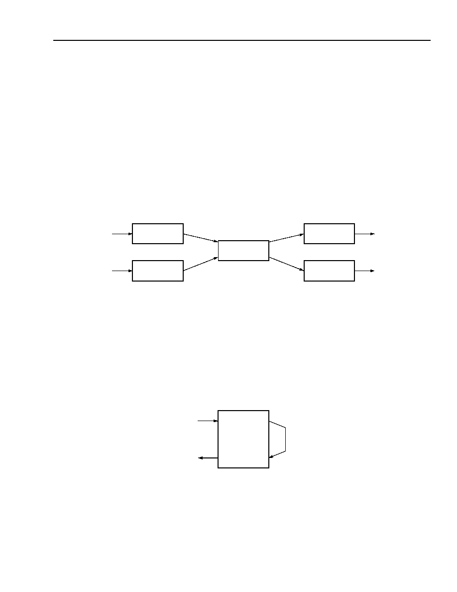
Agere Systems Inc.
47
Preliminary Data Sheet
August 2001
T1/E1/J1/J2 ATM Processor
TAAD08JU2 Newport
11 Applications
(continued)
11.3 Low-Speed ATM Access
In this application, data from a variety of sources are multiplexed into AAL2 using I.366.1 QoS MUXing. I.366.1
pertains only to the AAL type 2 and defines SSCS, CPCS, and SAR services necessary for mapping larger pack-
ets (e.g., >64 octets) to/from AAL2 VCs. Newport provides support for I.366.1 concentration to enable ATM trans-
port of a variety of low-speed services.
11.4 AAL2 Crossconnect
CID switching is provided by the following architecture. One (west) Newport device terminates an AAL2 VC,
demultiplexes CIDs from the CID into AAL0 cells, routes the AAL0 cells through a space switch fabric to a second
(east) Newport device. The east Newport device accepts the AAL0 cells, relates them to specific AAL2 VCs, and
maps the SSCS into CIDs and subsequently into an AAL2 VC and onto the physical transmission link. In this fash-
ion, Newport may function as a scalable AAL2 crossconnect by expansion in ports and (cell) switching fabric.
Note: East CIDs need not match west CIDs.
5-9976(F)
Figure 14. AAL2 Cross-Connect
In a fashion similar to the APC stand-alone ATM switching configuration, Newport may provide a stand-alone AAL2
cross-connect, as illustrated in Figure 15.
5-9977(F)
Figure 15. Stand-Alone AAL2 Cross-Connect
AAL2 VC_1
CIDs: A, C, B
AAL2 VC_2
CIDs: E, F, G
AAL2 VC_3
CIDs: A, E, B
AAL2 VC_4
CIDs: F, G, B
NEWPORT
(WEST)
NEWPORT
(WEST)
(ASX/ASE)
NEWPORT
(EAST)
NEWPORT
(EAST)
AAL0 VC_E
AAL0 VC_F
AAL0 VC_G
AAL0 VC_A
AAL0 VC_B
AAL0 VC_C
AAL2 V C_1
CIDs: A, C, B
AAL2 V C_2
CIDs: E, F, G
AAL0 VC_A
AAL0 VC_B
AAL0 VC_C
NEWPORT

48
Agere Systems Inc.
Preliminary Data Sheet
August 2001
T1/E1/J1/J2 ATM Processor
TAAD08JU2 Newport
12 Submodule Functional Description
12.1 Embedded Device Controller (EDC)
12.1.1 Introduction
The embedded device controller is based on an ARM9* RISC architecture. The EDC is responsible for the control
functions of Newport and is responsible for configuration, on-chip resource management, and compilation of statis-
tical information for performance monitoring. The EDC also provides alarm correlation among the blocks for faster
fault detection and isolation.
The EDC enables Newport to be controlled via high-level, simple, device-specific commands issued from the exter-
nal host device. The commands and associated parameters are converted into a series of register level transac-
tions for OAMP of blocks within the device.
The EDC also decouples host signaling insertion/extraction from the dataflow to enable scheduling of service to the
external device.
Through the use of embedded application code running on the EDC and APIs running on the external host device,
the Newport user achieves faster time-to-market with a powerful software architecture to control the highly inte-
grated system-on-a-chip device.
12.1.2 Features
!
Enables an abstract command/indication interface to Newport.
!
Performs alarm correlation and fault isolation without requiring external host intervention to minimize data loss.
!
Contains all necessary application code to provide its functions.
!
Allows data transfers between the host interface and the APC and SAR blocks to support implementation of
OAM functions on the host processor.
12.1.3 EDC Functional Description
The EDC contains an ARM core and a number of peripherals:
!
The arbiter and decoder.
!
Interfaces to embedded memories including two 32K x 32 SRAMs.
!
A programmable interrupt controller (PIC).
!
A timer block which provides a watchdog timer and seven additional general-purpose timers.
!
The host controller which can transfer between the ARM BUS and its own data buffers.
12.1.4 Host Interface
The host interface controller provides the interface between Newport and a host processor. This interface imple-
ments the host signal interface and registers through which the host communicates with Newport. A description of
the various data transfer protocols is contained in the firmware section of this document. The interface also pro-
vides the synchronization between the host clock (HCLK) and the chips global clock (GCLK).
The host registers are located in the HCLK domain to allow for very fast access reads. The input buffer is also writ-
ten using this clock. Any other signals that must pass to Newport's global clock are appropriately synchronized.
The synchronization scheme allows the global chip clock to be completely independent of HCLK.
* ARM is a registered trademark of Advanced Risc Machine Ltd.

Agere Systems Inc.
49
Preliminary Data Sheet
August 2001
T1/E1/J1/J2 ATM Processor
TAAD08JU2 Newport
12 Submodule Functional Description
(continued)
12.1.5 Host Interface Signals and Timing
The host interface mimics the timing of a sync-burst SRAM. All inputs and outputs are timed relative to the rising
edge of the host interface clock (HCLK). The data is delayed (by two clock cycles) relative to the corresponding
address so that reads and writes have exactly the same timing. This allows the user to easily interleave reads and
writes to Newport.
Another feature of the host interface is the HADV input, which allows the user to autoincrement the previously pro-
vided address rather than specifying a new address. This may be useful for users who wish to use the input and
output buffers in their linearly addressed mode.
1417 (F)
Figure 16. Standard Host Interface Timing
RA2
WA2
WA1
RA1
W1
R1
R2
W2A
W2B
W2C
W2D
R3
RA3
HCLK
HCEN
HADV
HA
HWEN
HD(31:0)
R3A

50
Agere Systems Inc.
Preliminary Data Sheet
August 2001
T1/E1/J1/J2 ATM Processor
TAAD08JU2 Newport
12 Submodule Functional Description
(continued)
12.1.6 Host Interactions
The host interface controller has several registers and two data buffers that are used for all external host communi-
cation. Addresses are shown per 32-bit word.
The host registers are shown in Table 14.
Table 14. Host Registers
Register Name
HA(9:0)
Bits
Reset
Value
Description
CONF (configuration)
0x000
0
0
SOFT_RESET. Places entire Newport device (except
for the host interface) into a reset state.
1
0
ARM_ENABLE. Allows the embedded ARM processor
to come out of reset. This bit should remain 0 until the
ARM's firmware has been loaded.
2
0
DCLK_RATE. Sets the rate of the clock to the framer,
TC, and IMA blocks (called DCLK):
0 = DCLK is equal to GCLK.
1 = DCLK is 1/2 of GCLK.
Normally, this bit is sent to 0.
3
0
DCLK_DISABLE. 1 disables the clock to the framer,
TC, and IMA blocks.
4
0
Reserved; should be set to 0.
31:5
0
Reserved.
IS (interrupt status)
0x001
0
0
1
IBRI (input buffer ready interrupt). Becomes active
when the host can write to the input buffer and the
command register.
1
0
OBRI (output buffer ready interrupt). Becomes active
when the output buffer and/or the indication register
has data for the host.
3:2
0
Reserved.
4
0
ASI0 (application-specific interrupt). Becomes active
when the ARM sets the register. Application-specific
interrupts are reserved for future use by the firmware.
5
0
ASI1(application-specific interrupt). Becomes active
when the ARM sets the register.
31:6
0
Reserved.
QIS (qualified interrupt
status)
0x002
31:0
0
This register contains the same bits as the interrupt
status register, after they have been qualified (ANDed)
by the corresponding bits in the interrupt enable regis-
ter.
IE (interrupt enable)
0x003
31:0
0
Each bit in this register is an enable for the corre-
sponding bit in the IS register. The IRQN signal
becomes active if the OR of each bit of (IS AND IE) is
active.
IES (interrupt enable set)
(write only)
0x004
31:0
--
During a write, a 1 in any data bit will cause the corre-
sponding bit in the interrupt enable register to be set.
IEC (interrupt enable
clear) (write only)
0x005
31:0
--
During a write, a 1 in any data bit will cause the corre-
sponding bit in the interrupt enable register to be
cleared.

Agere Systems Inc.
51
Preliminary Data Sheet
August 2001
T1/E1/J1/J2 ATM Processor
TAAD08JU2 Newport
12 Submodule Functional Description
(continued)
CMD (command
register)
0x006
31:0
0
The host should write commands to this register, which
will cause an interrupt to the ARM.
AIB (autoincrement input
buffer)
0x007
31:0
0
This address provides an autoincrementing address-
ing of the input buffer. This can be used in place of the
HADV external signal to write multiple 32-bit words to
Newport's host input buffer. The first write to this loca-
tion (after reset and after the Input buffer ready inter-
rupt has been sent) will be equivalent to a write-to
location 0x100. Subsequent writes will be to subse-
quent word addresses.
AWA (ARM processor
bus write address)
0x008
31:0
0
This register is used for downloading EDC firmware to
the ARM processor. A write to this register initiates a
write transfer from the host buffer to the address spec-
ified. The AWP register should be programmed before
writing to this location.
AWP (ARM processor
bus write
parameters)
0x009
8:0
0
This register is used for downloading EDC firmware to
the ARM processor. ARM processor bus transfer size:
specifies amount of data (in words) that should be
transferred to the ARM processor bus.
16:9
0
Input buffer start location. Starting location (in words)
of the input buffer from where the transfer should origi-
nate.
31:17
0
Reserved.
IBL (input buffer level)
0x00A
8:0
0
READ-ONLY. The host can read this register to deter-
mine how much data is present in the input buffer. This
is only updated when the host is writing data and after
the entire buffer of data has been transferred out of the
buffer.
31:9
0
Reserved.
IR (indication register)
0x00B
31:0
0
READ-ONLY. The host can read this register after the
arm has set the output buffer ready interrupt.
AOB (autoincrement out-
put buffer)
0x00C
31:0
0
READ-ONLY. This location provides an autoincrement-
ing addressing of the output buffer. This can be used in
place of the HADV external signal to read multiple
32-bit words from Newport's host output buffer. The
first read from this location (after reset and after the
output buffer ready interrupt has been set) will be
equivalent to a read from location 0x200. Subsequent
reads will be from subsequent word addresses.
ARA (ARM processor
bus read address)
0x00D
31:0
0
This register is a diagnostic register that allows the
host to read back the contents of the ARM processor
memories. A write to this register initiates an ARM pro-
cessor bus read transfer from the ARM processor bus
address specified to the host output buffer. The AWP
register should be programmed before writing to this
location.
Table 14. Host Registers (continued)
Register Name
HA(9:0)
Bits
Reset
Value
Description

52
Agere Systems Inc.
Preliminary Data Sheet
August 2001
T1/E1/J1/J2 ATM Processor
TAAD08JU2 Newport
12 Submodule Functional Description
(continued)
ARP (ARM processor
bus read parameters)
0x00E8
8:0
0
This register is a diagnostic register that allows the
host to read back the contents of the ARM processor
memories. ARM processor bus transfer size: specifies
amount of data (in words) that should be transferred
from the ARM processor bus.
16:9
0
Output buffer start location. Starting location (in words)
of the output buffer to where the transfer should go.
31:17
0
Reserved.
OBL (output buffer level)
0x00F
8:0
0
READ-ONLY. The host can read this register to deter-
mine how much data is present in the output buffer.
This is only updated after the entire transfer of data
into the buffer.
31:9
0
Reserved.
VR (version register)
(This entire 32 bit regis-
ter provides the same
value as the device ID
accessible through the
JTAG.)
0x010
11:0
0x03B ID number + LSB of 1.
27:12 0x5A94 Part number.
31:28
X
Version number. Varies with each mask set.
BIST_INPUT_BUFFER
0x011
31:0
0
Reserved; must be set to 0.
IB (0:255) (input buffer)
0x100-
0x1FF
31:0
--
Linearly addressed input buffer.
OB (0:255) (output
buffer)
0x200-
0x2FF
31:0
--
Linearly addressed output buffer.
1
Note: The reset value of 0 is present while the internal reset is active. When the internal reset goes inactive, this bit will become active to sig-
nify that the ARM booting can commence.
Table 14. Host Registers (continued)
Register Name
HA(9:0)
Bits
Reset
Value
Description

Agere Systems Inc.
53
Preliminary Data Sheet
August 2001
T1/E1/J1/J2 ATM Processor
TAAD08JU2 Newport
13 Framer Block
13.1
Introduction
The framer block implements the physical layer function in the ATM protocol stack. The block interfaces with the
T1/E1/J1/J2 lines on the line side and the TC block on the system side. It also has a CHI interface for carrying TDM
traffic. The block receives and transmits data traffic available from the ATM or TDM interfaces over the physical
line. It also receives and transmits data link information over the line.
The framer block is a flexible framer engine that enables integration of a feature-rich, yet power-efficient framer
function into Newport.
13.2 Features
!
Framer features:
-- T1 framing modes: ESF, D4, SLC*-96, T1 DM DDS, SF (F1-only)
-- E1 framing modes: G.704 basic and CRC-4 multiframe consistent with G.706
-- J1 framing modes: JESF (Japan)
-- J2 framing modes: NTT and TTC framing/overhead support
-- E1 signaling modes:
Ę Transparent
Ę Register and system access for entire TS16 multiframe structure per ITU G.732
Ę Alarm reporting and performance monitoring per AT&T, ANSI, ITU-T, NTT, TTC, and ETSI standards
!
Facility data link features:
-- HDLC or transparent access for either ESF or DDS+ FDL frame formats
-- Register/stack access for SLC-96 transmit and receive data
-- Extended superframe (ESF):
-- Automatic transmission of the ESF performance report messages (PRM)
-- Automatic transmission of the ANSI T1.403 ESF performance report messages
-- Automatic detection and transmission of ANSI T1.403 ESF FDL bit-oriented codes
-- Register/stack access for all CEPT Sa-bits transmit and receive data
!
HDLC features:
-- HDLC or transparent mode
-- Programmable logical channel assignment: any time slot, any bit for ISDN D-channel, also inserts/extracts C-
channels for V5.1 and V5.2 interfaces
-- 64 logical channels in both transmit and receive direction (any framing format)
-- Maximum channel data rate: 64 kbits/s
-- Minimum channel data rate: 4 kbits/s (DS1-FDL or E1 Sa bit)
-- 128-byte FIFO per channel in both transmit and receive direction
-- Tx to Rx loopback supported
!
System interfaces:
-- Concentration highway interface:
Ę Single clock and frame sync signals
Ę Programmable clock rates at 2.048 MHz, 4.096 MHz, 8.192 MHz, and 16.384 MHz
Ę Programmable data rates at 2.048 Mbits/s, 4.096 Mbits/s, and 8.192 Mbits/s
Ę Programmable clock edges and bit/byte offsets
-- LIU interface
Ę 8 T1/E1/J1 channels
Ę 4 J2 (6.312-Mbits/s) channels
Ę Line coding: B8ZS, HDB3, AMI, and CMI (JJ20-11)
* SLC is a registered trademark of Lucent Technologies Inc.

54
Agere Systems Inc.
Preliminary Data Sheet
August 2001
T1/E1/J1/J2 ATM Processor
TAAD08JU2 Newport
13 Framer Block
(continued)
13.3 Framer-to-Line Interface Unit Physical Interface
The network interface of the framer consists of eight groups of six connections. The six connections for each
framer are TND, TPD, and TLCK, driven from the transmit framer (receive path), and RPD, RND, and RCLK (trans-
mit path), sourced from the external line interface device.
The line interface may operate in single rail or dual rail mode. The default mode of the line encoder is single-rail. In
this mode, the input signals are passed transparently through the line encoder.
In single rail mode, the link's framer internal bipolar line encoder/decoder is disabled and monitoring of received
line format violation is accomplished with the use of the RND input. When RND = 1 on the rising edge of RLCK, the
line format violation counter increments by one. The link's transmit framer transmits data via the TPD output pin
while TND is forced to a 0 state.
In dual rail mode, the internal line encoder/decoder and monitoring are enabled. The line code may be selected
from the following choices:
!
Alternate mark inversion (AMI).
!
High-density bipolar of order 3--G.703, A.1 (HDB3).
!
Binary 8 zero code suppression--G.703, A.2 (B8ZS).
Line format violations due to excessive zeros will be optionally monitored as follows:
!
B8ZS--8 consecutive zeros cause a violation.
!
HDB3--4 consecutive zeros cause a violation.
13.3.1 Clocking Modes
This section lists all the Tx Line clocking modes for framer.
!
Mode A1: either All E1s or all T1s or all J2s running of a single clock (just ATM traffic). In this mode, the CRXCLK
input will be used to drive the Tx line clocks. The CRXCLK input can be 1.544 Mhz (T1), 2.048 Mhz (E1), or
6.312 Mhz (J2). Only ATM traffic is supported in this mode. Note that a maximum of four J2 lines are supported
in this mode.
!
Mode A2: a mix of E1s and T1s--all E1s running off a single clock, all T1s running off another single clock (just
ATM traffic). In this mode, a reference 2.048 Mhz clock input on CRXCLK is used to feed into a PLL that gener-
ates 1.544 Mhz and 2.048 Mhz. The two clocks will be then selected on a per-link basis to run the line at either
E1 or T1 rate. Only ATM traffic is supported in this mode.
Note: Newport does not allow a mix of J2s with either E1s or T1s.
!
Mode A3: independent timing--8 independent clock inputs will be used to drive the 8 lines (just ATM traffic). In
this mode, 8 independent (mutually asynchronous) clocks will be input to the framer. These clocks will be used to
drive the Tx line clocks for each line (LTXCLK).
Note: In this mode LTXCLK is an input). Only ATM traffic is supported in this mode.
!
Mode A4: loop timing--the Rx line clock will be used to drive the Tx line clocks (just ATM traffic). In this mode,
the Rx line clocks (LRXCLK) get internally looped to the Tx line clock (LTXCLK). Only ATM traffic is supported in
this mode.
!
Mode B1: either All E1s or all T1s running of a single clock or a mix of E1s and T1s--all E1s running off a single
clock, all T1s running off another single clock (ATM plus CHI traffic). In this mode, the receive CHI clock (CRX-
CLK) is used to feed in to the PLL which generates a 1.544 Mhz clock and a 2.048 Mhz clock. These clocks are
then selected on a per-link basis to run the line at either E1 or T1 rate. Both ATM and CHI traffic are supported in
this mode.

Agere Systems Inc.
55
Preliminary Data Sheet
August 2001
T1/E1/J1/J2 ATM Processor
TAAD08JU2 Newport
13 Framer Block
(continued)
13.4 Frame Formats
The eight framers support the following frame formats:
!
DS1 superframe D4.
!
DS1 superframe J-D4 with Japanese Remote Alarm.
!
DS1 superframe DDS.
!
DS1 superframe SLC-96.
!
DS1 extended superframe (ESF).
!
Japanese extended superframe J-ESF (J1 standard with different CRC-6 algorithm).
!
Non-align DS1 (transparent 193 bits).
!
CEPT basic frame {ITU G.706}.
!
CEPT CRC-4 multiframe with 100 ms timer (ITU G.706).
!
CEPT CRC-4 multiframe with 400 ms timer (automatic CRC-4/nonCRC-4 equipment interworking) (ITU G.706
Annex B).
!
Nonalign E1 (transparent 256 bits).
!
2.048 coded mark inversion (CMI) coded interface (TTC Standards JJ-20.11).
!
6.312 Mbits/s interface (ITU G.704/NTT J2).

56
Agere Systems Inc.
Preliminary Data Sheet
August 2001
T1/E1/J1/J2 ATM Processor
TAAD08JU2 Newport
13 Framer Block
(continued)
13.5 Transmit Framer Functions
!
Transmits alarm indication signal (AIS) to the line automatically and on demand.
!
Transmits AIS-CI to the line automatically and on demand.
!
Transmits remote alarm indication (RAI) to the line automatically and on demand. Conditions for transmitting RAI
include; loss of received frame alignment, CEPT loss of received time slot 0 multiframe alignment, CEPT CRC-4
timer expiration, CEPT loss of received time slot 16 signaling multiframe alignment, CEPT received Sa6 equals
8, and received Sa6 equals C.
!
Transmits RAI-CI to the line automatically and on demand.
!
Transmits auxiliary test pattern (AUXP) to the line automatically and on demand.
!
Transmits CEPT E bits based received CRC-4 errors.
!
Support the CEPT double not-FAS system mode.
!
Transmits line loopback on and off codes to the line on demand (T1.403 section 9.3.1).
!
When not in frame alignment, to optionally send AIS or transparently pass data.
13.6 DS1 Transparent Framing Format
The transmit framer can be programmed to transparently transmit 193 bits of CHI data to the line.
When configured for transparent framing, the transmit framer extracts bit 8 of time slot 1 from the receive CHI data
and inserts this bit into the framing bit position of the transmit line data. The other 7 bits of the receive system time
slot 1 are ignored by the transmit framer. The receive framer will insert every 193rd bit of the receive line data into
bit 8 of time slot 1 of the CHI data. The other bits of time slot 1 are set to 0.
Frame integrity is maintained in both the transmit and receive framer sections.

Agere Systems Inc.
57
Preliminary Data Sheet
August 2001
T1/E1/J1/J2 ATM Processor
TAAD08JU2 Newport
13 Framer Block
(continued)
5-5989(F).ar.1
Figure 17. DS1 Transparent Frame Structure
In transparent framing mode 1, the receive framer is forced not to reframe on the receive line data. Other than
bipolar violations and unframed AIS monitoring, there is no processing of the receive line data. The receive framer
will insert the 193rd bit of the receive line data into bit 8 of time slot 1 of the transmit system data.
Bit 8 of time slot 1 of the receive system interface is inserted as the 193rd data bit into the transmit line data.
In transparent framing mode 2, the receive framer functions normally on receive line data. All normal monitoring of
receive line data is performed, and data is passed to the transmit CHI as programmed. The receive framer inserts
the extracted framing bit of the receive line data into bit 8 of time slot 1 of the transmit system data. The remaining
bits in time slot 1 are set to 0.
Bit 8 of time slot 1 of the receive system interface is inserted in the transmit line framing bit position.
13.7 CEPT 2.048 Basic Frame Structure Transparent Framing Format
The transmit framer can be programmed to transparently transmit 256 bits of CHI data to the line. The transmit
framer must be programmed to transparent framing mode 1.
In transparent mode, the transmit framer transmits all 256 bits of the system payload unmodified to the line. Time
slot 1 of the CHI interface, determined by the system frame sync signal, is inserted into the FAS/NOTFAS time slot
of the transmit line interface.
Frame integrity is maintained in both the transmit and receive framer sections.
5-5988(F)
Figure 18. CEPT Transparent Frame Structure
TIME SLOT 1
(STUFF TIME SLOT)
32 TIME-SLOT CHI FRAME
TIME SLOT 2 TIME SLOT 3
TIME SLOT 31 TIME SLOT 32
0
0
0
0
0
0
0
F BIT
TRAMSMIT FRAMER'S
193-bit FRAME
DS1 = 125
Ą
s
TIME SLOT 1 TIME SLOT 2
TIME SLOT 24
F BIT
TIME SLOT 1
32 TIME-SLOT CHI FRAME
TIME SLOT 2 TIME SLOT 3
TIME SLOT 31 TIME SLOT 32
TIME SLOT 1
32 TIME-SLOT LINE FRAME
TIME SLOT 2 TIME SLOT 3
TIME SLOT 31 TIME SLOT 32

58
Agere Systems Inc.
Preliminary Data Sheet
August 2001
T1/E1/J1/J2 ATM Processor
TAAD08JU2 Newport
13 Framer Block
(continued)
In transparent framing mode 1, the receive framer is forced not to reframe on the receive line data. Other than bipo-
lar violations and unframed AIS monitoring, there is no processing of the receive line data. The entire receive line
payload is transmitted unmodified to the CHI.
In transparent framing mode 2, the receive framer functions normally on the receive line data. All normal monitor-
ing of receive line data is performed, and data is transmitted to the CHI as programmed.
13.8 Receive Framer Nonalignment Mode (DS1/E1)
In the nonalign framing modes, the receive frame aligner does not frame to the receive line data. Other than bipolar
violations, AIS, and AUXP monitoring, there is no processing of the receive line data. The entire receive line frame
is given unmodified to the system interface.
13.9 Loss of Frame Alignment Criteria
There are two criteria for declaring loss of frame; frame bit errors and CRC errors.
13.9.1 Frame Bit Errors
!
T1: 2 frame bit errors out of 4 frame bits (F
T
and F
S
bits checked).
!
T1: 2 frame bit errors out of 5 frame bits (F
T
and F
S
bits checked).
!
T1: 2 frame bit errors out of 6 frame bits (F
T
and F
S
bits checked).
!
T1: 3 frame bit errors out of 12 frame bits--DDS only (F
T
, F
S
, and time slot 24 F bits).
!
T1: 2 frame bit errors out of 4 frame bits (only F
T
bits checked).
!
T1: 2 frame bit errors out of 5 frame bits (only F
T
bits checked).
!
T1: 2 frame bit errors out of 6 frame bits (only F
T
bits checked).
!
T1: 4 frame bit errors out of 12 frame bits--DDS only (F
T
, F
S
, and time slot 24 FAS pattern).
!
E1: 3 consecutive incorrect frame alignment signals.
!
E1: 3 consecutive incorrect frame alignment signals or 3 consecutive incorrect non-FAS frames as indicated by
bit 2 in time slot 0 in frames not containing the frame alignment signal.
!
E1: 3 consecutive incorrect FAS or non-FAS frames.
!
2.048 Mbits/s CMI: 2 consecutive missing code rule violations (CRVs).
13.9.2 CRC Errors
!
The use of CRC errors to declare loss of frame is optional. CRC errors are monitored in the performance monitor
block.
!
In DS1 mode, ESF, and J-ESF formats only, N or more CRC-6 errors in a 1 second interval results in loss of
frame alignment. N is provisionable. N defaults to 320 in DS1 mode.
!
In CEPT mode N, or more, CRC-4 errors in a 1 second interval results in loss of frame alignment. N is provision-
able. N defaults to 915 in CEPT modes.
13.10 Frame Alignment Criteria
Table 15 describes the frame alignment criteria for the formats supported by the framer.

Agere Systems Inc.
59
Preliminary Data Sheet
August 2001
T1/E1/J1/J2 ATM Processor
TAAD08JU2 Newport
13 Framer Block
(continued)
Table 15. Frame Alignment Criteria
13.11 Performance Monitoring Functional Integration Into Framer
The framer monitors the recovered line data for alarm conditions and errored events. To a lesser degree of impor-
tance, the framer also monitors the receive system data when in the switching mode and presents the information
to the system through the embedded device controller.
In the transport mode, both directions are monitored for alarm conditions and error events.
Table 16 shows the functions provided by the performance monitor and establishes the functions' validity in partic-
ular framing modes.
Frame Format
Alignment Procedure
SF
Frame alignment is established when six consecutive error-free superframes are
received. Only the F
T
framing bits are checked (36 bits checked).
D4 and J-D4
Frame alignment is established when six consecutive error-free superframes are
received (72 bits checked in D4, 66 bits checked in J-D4).
DDS
Frame alignment is established when six consecutive error free frames are
received (42 bits checked: F
T
, F
S
, and time slot 24).
SLC-96
The F
T
frame position is established when four consecutive error-free super-
frames are received (24 F
T
bits checked). After establishing the F
T
frame posi-
tion, SLC-96 superframe alignment is established on the first valid F
S
sequence
of 000111000111. All the while the F
T
frame position must remain error free.
ESF and J-ESF
Frame alignment is established when three consecutive error-free superframes
are received (18 bits checked).
CEPT Basic
Frame
Uses the strategy outlined in G.706 paragraph 4.1.2.
CEPT CRC-4
100 ms Timer
Uses the strategy outlined in G.706 paragraphs 4.1.2 and 4.2.
CEPT CRC-4
400 ms Timer
Uses the strategy outlined in G.706 paragraph 4.1.2 and Annex B.
2.048 Mbits/s CMI
Coded Interface
Frame alignment is established on the first detection of the CRV violation. Multi-
frame alignment is achieved the first time the 01111111 multiframe alignment pat-
tern is detected.

60
Agere Systems Inc.
Preliminary Data Sheet
August 2001
T1/E1/J1/J2 ATM Processor
TAAD08JU2 Newport
13 Framer Functional Description
(continued)
Table 16. Performance Monitor Functional Descriptions
Function
Description
Valid Framing Modes for
Functions
1
Performance report messages (PRMs) as per G.704 section
2.1.3.1.3.3, G.963, T1.231 section 6.3, and T1.403 section 9.4.2.
ESF and J-ESF only
2
Provides status for errored seconds, bursty errored seconds,
severely errored seconds, and unavailable seconds at ET, ET-
RE, NT, and NT-RE.
All modes
3
Maintains a count of errored seconds, bursty errored seconds,
severely errored seconds, and unavailable seconds at the ET.
All modes
4
Provides a status indication for a loss of signaling frame align-
ment condition.
All modes
5
Provides a status indication for an out of frame condition.
All modes
6
Provides a status indication for a loss of time slot 0 CRC-4 multi-
frame alignment.
CEPT CRC-4 only
7
Provides a status indication for a time slot 0 CRC-4 multiframe
alignment signal bit error.
CEPT CRC-4 only
8
Provides a status indication for auxiliary pattern detection.
CEPT CRC-4 only
9
Provides a status indication for detection of the DS1 idle signal.
All modes except CEPT CRC-4
10
Provides a status indication for detection of an alarm indication
signal.
All modes
11
Provides a status indication for detection of an alarm indication
signal at the customer installation (AIS-CI).
All modes except CEPT-CRC4
12
Provides a status indication for detection of remote alarm indica-
tion.
All modes
13
Provides a status indication for detection of remote alarm indica-
tion at the customer installation (RAI-CI).
ESF and J-ESF only
14
Provides a status indication for detection of time slot 16 AIS.
CEPT CRC-4 only
15
Provides a status indication for detection of remote multiframe
alarm in time slot 16 (RTS16MFA).
CEPT CRC-4 only
16
Provides a status indication for the loss of CEPT biframe align-
ment (LBFA).
CEPT CRC-4 only
17
Provides a status indication for detection of remote Japanese
yellow alarm (RJYA).
J-D4 only
18
Provides a status indication for continuous E-bit reception.
CEPT CRC-4 only
19
Provides a status indication for detection of Sa6 states.
CEPT CRC-4 only
20
Provides a status indication for detection of line format violations. All modes
21
Provides a status indication for detection of frame bit errors.
All modes
22
Provides a status indication for detection of CRC errors.
ESF, J-ESF, and CEPT CRC-4
only
23
Provides a status indication for detection of excessive CRC
errors.
ESF, J-ESF, and CEPT CRC-4
only
24
Provides a status indication for detection of an E bit equal to 0.
CEPT CRC-4 only
25
Provides a status indication for expiration of CRC-4 multiframe
alignment timer.
CEPT CRC-4 only
26
Provides a status indication for new frame alignment.
All modes
27
Provides a status indication for detection of Sa7 link identification
code.
CEPT CRC-4 only

Agere Systems Inc.
61
Preliminary Data Sheet
August 2001
T1/E1/J1/J2 ATM Processor
TAAD08JU2 Newport
13 Framer Block
(continued)
28
Provides a status indication for detection of an SF line loopback
on code.
SF only
29
Provides a status indication for detection of an SF line loopback
off code.
SF only
30
Provides a status indication for detection of an overflow in the
receive elastic store.
All modes
31
Provides a status indication for detection of an underflow in the
receive elastic store.
All modes
32
Provides a status indication for detection of loss of signal.
All modes
33
Maintains a count of received CRC errors.
ESF/J-ESF and CEPT CRC-4 only
34
Maintains a count of received bipolar violations, line code viola-
tions, and excessive zeros.
All modes
35
Provides a status indication for detection of a bit oriented mes-
sage in the ESF data link bits.
ESF only
36
Provides a status indication of a test pattern detector lock.
All modes
37
Provides a status indication for detection of a test-pattern bit
error.
All modes
38
Provides a status indication for detection of an ESF-FDL RAI/yel-
low alarm code.
ESF only
39
Provides a status indication for detection of the ESF-FDL pay-
load loopback enable code.
ESF only
40
Provides a status indication for detection of the ESF-FDL pay-
load loopback disable code.
ESF only
41
Provides a status indication for detection of the ESF-FDL line
loopback enable code.
ESF only
42
Provides a status indication for detection of the ESF-FDL line
loopback disable code.
ESF only
43
Maintains a 16-bit count of received framing bit errors.
All modes
44
Maintains a 16-bit count of received E bit = 0 events.
CEPT CRC-4 only
45
Maintains a 16-bit count of received Sa6 = 00x1 events.
CEPT CRC-4 only
46
Maintains a 16-bit count of received Sa6 = 001x events.
CEPT CRC-4 only
47
Provides a status indication for detection of an (A, Sa5, Sa6[1:4])
= (x, x, AIS).
CEPT CRC-4 only
48
Provides a status indication for detection of an (A, Sa5, Sa6[1:4])
= (0, 1, 1111).
CEPT CRC-4 only
49
Provides a status indication for detection of an (A, Sa5, Sa6[1:4])
= (1, 1, 1111).
CEPT CRC-4 only
50
Provides a status indication for detection of an (A, Sa5, Sa6[1:4])
= (x, x, AUXP).
CEPT CRC-4 only
51
Provides a status indication for detection of an (A, Sa5, Sa6[1:4])
= (1, 1, 1000).
CEPT CRC-4 only
52
Provides a status indication for detection of an (A, Sa5, Sa6[1:4])
= (0, 1, 1000).
CEPT CRC-4 only
53
Provides a status indication for detection of an (A, Sa5, Sa6[1:4])
= (0, 1, 1110).
CEPT CRC-4 only
Table 16. Performance Monitor Functional Descriptions (continued)
Function
Description
Valid Framing Modes for
Functions

62
Agere Systems Inc.
Preliminary Data Sheet
August 2001
T1/E1/J1/J2 ATM Processor
TAAD08JU2 Newport
13 Framer Block
(continued)
13.12 Performance Report Message
A performance report message is assembled by the performance monitoring block in the framer. This message can
be either sent automatically in the ESF data link or sent as a result of a command. The performance monitor block
monitors for errored second events and generates the one-second data for the extended superframe (ESF) perfor-
mance report message (PRM) (G.704 section 2.1.3.1.3.3, G.963, T1.231 section 6.3, and T1.403 section 9.4.2).
The form of the PRM message is shown in Table 17 below. The definition of the fields is given in Table 17.
A severely errored frame (SEF) defect is determined by examining contiguous time windows for frame bit errors. In
ESF, the window size is 3 ms, and only the frame pattern sequence bits are checked. An SEF defect occurs when
two or more frame bit errors in a window are detected. An SEF defect is terminated when the signal is in frame and
there are less than two frame bit errors in a window.
Table 17. Performance Report Message Format
54
Provides a status indication for detection of an (A, Sa5, Sa6[1:4])
= (0, 1, 1100).
CEPT CRC-4 only
55
Provides a status indication for detection of an (A, Sa5, Sa6[1:4])
= (1, 0, 0000).
CEPT CRC-4 only
56
Provides a status indication for detection of an (A, Sa5, Sa6[1:4])
= (1, 1, 1110).
CEPT CRC-4 only
57
Provides a status indication for detection of an (A, Sa5, Sa6[1:4])
= (1, 1, 00xx).
CEPT CRC-4 only
58
Provides a status indication for detection of an (A, Sa5, Sa6[1:4])
= (x, 0, xxxx).
CEPT CRC-4 only
Octet Number
PRM B7 PRM B6 PRM B5 PRM B4 PRM B3 PRM B2 PRM B1 PRM B0
1
Flag
2
SAPI
C/R
EA
3
TEI
EA
4
Control
5
G3
LV
G4
U1
U2
G5
SL
G6
6
FE
SE
LB
G1
R
G2
Nm
NI
7
G3
LV
G4
U1
U2
G5
SL
G6
8
FE
SE
LB
G1
R
G2
Nm
NI
9
G3
LV
G4
U1
U2
G5
SL
G6
10
FE
SE
LB
G1
R
G2
Nm
NI
11
G3
LV
G4
U1
U2
G5
SL
G6
12
FE
SE
LB
G1
R
G2
Nm
NI
13--14
FCS
15
FLAG
Table 16. Performance Monitor Functional Descriptions (continued)
Function
Description
Valid Framing Modes for
Functions

Agere Systems Inc.
63
Preliminary Data Sheet
August 2001
T1/E1/J1/J2 ATM Processor
TAAD08JU2 Newport
13 Framer Block
(continued)
.
Table 18. Performance Report Message Field Definition
Field
Definition
G1 = 1
CRC Error Event = 1
G2 = 1
1 < CRC Error Event
5
G3 = 1
5 < CRC Error Event
10
G4 = 1
10 < CRC Error Event
100
G5 = 1
100 < CRC Error Event
319
G6 = 1
CRC Error Event
320
SE = 1
Severely Errored Framing Event
1 (FE will = 0)
FE = 1
Frame Synchronization Bit Error Event
1 (SE will = 0)
LV = 1
Line Code Violation Event
1 (BPV
1 or EXZ
1)
SL = 1
Slip Event
1
LB = 1
Payload Loopback Activated
U1, U2 = 0
Reserved
R = 0
Reserved (default value = 0)
Nm, NI = 00, 01, 10, 11
One Second Report Modulo 4 Counter

64
Agere Systems Inc.
Preliminary Data Sheet
August 2001
T1/E1/J1/J2 ATM Processor
TAAD08JU2 Newport
13 Framer Block
(continued)
13.13 ESF Data Link
When the framer is in ESF mode, several options are available for use of the 4 kbits/s data link that is part of the SF
framing structure. The NPT_PHY_FRAMER_AUTOPRM command allows for the enabling and disabling of auto-
matic sending of the PRM and the selection of threshold levels for the receive and transmit ESF data link FIFOs
from two choices programmed using the NPT_PHY_FRAMER_DL_THRESHOLDS command. If the PRM is set to
be transmitted automatically, then the data link cannot be used for other types of messages. If the automatic PRM
is disabled, the ESF data link channel can be used to send bit-oriented messages (BOMs), PRM, and any other
data message the user wishes to send. Messages to be sent are specified using the
NPT_PHY_FRAMER_DATA_LINK_MSG in the case of non-BOM or NPT_PHY_FRAMER_BOM command for
BOM. Non-BOM messages can be up to 128 bytes long. Received messages generate a
NPT_PHY_DATA_LINK_RCVD or NPT_PHY_BOM_RCVD indication for the host to extract the data.
13.14 Facility Data Link
The facility data link is available in SLC-96, DDS and CEPT framing formats. FDL messages are sent using the
NPT_PHY_FRAMER_FDL_STACK command and received using the NPT_PHY_FRAMER FDL RCVD indication.
13.15 Receive Data Link Functional Description
This block extracts facility data links bits, as follows:
!
D bits from the SLC-96 multi-superframe.
!
Sa bits from time slot 0 in CEPT basic and CRC-4 multiframes.
!
Data link bits from DDS frames.
The respective bits will always be extracted from the framed aligned receive line payload and stored in the facility
data link stack regardless of other configuration bits.

Agere Systems Inc.
65
Preliminary Data Sheet
August 2001
T1/E1/J1/J2 ATM Processor
TAAD08JU2 Newport
13 Framer Block
(continued)
All frame types:
!
Support clear-on-read status and interrupt bits based on the setting of the input select signal.
13.16 SLC-96 Superframe Receive Data Link
!
Delineates the SLC-96 data link in the Fs signaling frame, extracts the 24 D bits, and stores them in word 1 of
the NPT_PHY_FRAMER_FDL_RECEIVED indication.
!
Provides interrupt for stack ready.
!
Provides host access to stack using processor clock.
!
Supports loss of frame status.
Both basic frame alignment and multiframe alignment must be established before the data can be assumed valid.
13.17 DDS Receive Data Link Stack
!
Extracts data link bit (bit 6) from time slot 24 and stores it in words 1 and 2 of the
NPT_PHY_FRAMER_FDL_RECEIVED indication.
!
Provides interrupt via indication processing.
!
Provides host access to stack using NPT_PHY_FRAMER_FDL_RECEIVED indication.
!
Supports loss of frame status.
DDS frames are numbered 1 through 12 with the data link bits located in bit 6 of time slot 24 in every frame. Only
basic frame alignment must be established for the data link bits to be extracted.
13.18 CEPT; CEPT CRC-4 (100 ms); CEPT CRC-4 (400 ms) Multiframe Sa Bits Receive Stack
!
Extracts two multiframes of Sa bits from CEPT links and stores them in words 1 through 3 of the
NPT_PHY_FRAMER_FDL_RECEIVED indication.
!
Supports loss of frame status.
!
Provides host access to the stack using NPT_PHY_FRAMER_FDL_RECEIVED indication.
!
Provides interrupt via indication processing.
CEPT frames are numbered 0 through 15 with the Sa bits located in time slot 0 of the odd numbered frames. The
Sa bits can only be extracted from CEPT links when the proper alignment has been established.
For basic CEPT frames, the Sa bits will be extracted given the arbitrary alignment selected by the frame aligner
block when basic frame alignment is established. For CEPT CRC-4 links the Sa bits will be extracted based on the
alignment determined by the frame aligner block when multiframe frame alignment is established.
Optionally, the Sa bits will be extracted from CEPT CRC-4 links only after basic frame alignment is established
(RxCRCSM).
13.19 Receive Data Link Stack Idle Modes
!
No data link stack features for the following frame formats:
-- D4
-- J-D4
-- ESF
-- J-ESF
-- J2
-- CMI

66
Agere Systems Inc.
Preliminary Data Sheet
August 2001
T1/E1/J1/J2 ATM Processor
TAAD08JU2 Newport
13 Framer Block
(continued)
13.20 Transmit Facility Data Link Functional Description
This block performs the transmission of D bits into SLC-96 superframes, Sa bits into CEPT multiframes, and data-
link bits into DDS frames using the NPT_PHY_FRAMER_STACK command.
13.21 SLC-96 Superframe Transmit Data Link
!
Provides for sending D bits and delineator bits on SLC-96 bits via the NPT_PHY_FRAMER_STACK command.
!
Provides interrupt and initiates NPT_PHY_FRAMER_FDL_SENT indication process using a Tx threshold.
!
Performs retransmission of stack when update is yet to be performed.
The 12 frame SLC-96 superframe is composed of a terminal frame (F
T
) alternating with a subframe that consists of
a combined signaling (F
S
) frame and data link. The subframe shares establishing the signaling frame (F
S
) and
SLC-96 data link. The FDL stack bits are inserted into the signaling and data link subframe position in the super-
frame. Seventy-two frames (six superframes) are required to deliver the 24 D bits and 12-bit delineator. The front-
end delineator is 00111, which is followed by 24 D bits and trailed by 0001110. The alignment of the F
S
bits within
the superframe is determined and indicated by the frame aligner block.
The transmission of the SLC-96 stack will take 9 ms to complete, during which time the host should refill the stack
using the NPT_PHY_FRAMER_FDL_STACK command if the D bits need to change.
13.22 DDS Transmit Data Link Stack
!
Provides for sending three superframes of data link bits via the NPT_PHY_FRAMER_FDL_STACK command.
!
Provides interrupt and initiates NPT_PHY_FRAMER_FDL_SENT indication process using a Tx threshold.
!
Performs retransmission of stack when update has yet to be performed.
!
Provides host access to stack using NPT_PHY_FRAMER_FDL_STACK command.
The transmission of the SLC-96 stack will take 9 ms to complete, during which time the host should refill the stack
using the NPT_PHY_FRAMER_FDL_STACK command if the D bits need to change.
13.23 Transmit ESF Data Link Bit-Oriented Messages
!
Provides capability to transmit bit-oriented messages.
When enabled, bit-oriented messages will be transmitted on the data link channel of the frame bit for ESF links.
The ESF superframe is numbered 1 through 24 with the data link channel transmitted in the odd numbered frames
(4 kbits/s).
The BOM is a 16-bit message defining an alarm or command and response action, and sent repeatedly for a
period of time determined by the event. The message consists of eight 1s, a 0, a 6-bit code to identify the alarm or
action, and a 0 (1111_1111_0 in front and 0 behind the 6-bit code).

Agere Systems Inc.
67
Preliminary Data Sheet
August 2001
T1/E1/J1/J2 ATM Processor
TAAD08JU2 Newport
13 Framer Block
(continued)
The message can occur at any point in the extended superframe without respect to boundaries. The BOM format
is as follows:
0 X X X _ X X X 0 _ 1111_1111 (right-most bit being transmitted first).
When the BOM pattern is enabled, it will be transmitted until disabled. When disabled, the pattern will cease to be
transmitted immediately.
When enabled, the BOMs should only be inserted when the proper alignment has been reached. For ESF links,
both BFA and MFA are required for insertion. This condition effects the insertion of BOMs bits and the reporting of
stack empty to the host.
13.24 CEPT, CEPT Multiframe Transmit Data Link Sa Bits Stack
!
Provides two multiframes of Sa-bit storage for transmission on CEPT links.
!
Provides interrupt for stack empty.
!
Performs retransmission of stack when update has yet to be performed.
!
Provides capability to source Sa bits from blocks other than the data link block.
This block will always present the Sa bits stored in the Tx stack to the TDM data stream. In CEPT, the Sa bits are
located in time slot 0 of the NOTFAS frames (odd numbered frames). CEPT multiframe format frames are num-
bered 0 through 15 with the Sa bits located in time slot 0 of the odd numbered frames (NOTFAS frames).
The Sa bits are stored in the Tx stack as follows.
Table 19. Shared Tx Stack Format for CEPT Frame
Transmission of the Sa stack will take 4 ms, during which time the host should refill the system stack if the Sa bits
need to change.
Near the beginning of each CEPT double multiframe, the Tx data link block will determine whether a new set of Sa
bits is available to be transmitted. If this is the case, the new Sa bits will be transmitted; otherwise, the previous Sa
bits will be retransmitted.
When enabled, the Sa bits will only be inserted when the proper alignment has been reached. For CEPT with no
CRC-4 links, only biframe alignment (BFA) is required for insertion. For CEPT with CRC-4 links, both biframe align-
ment (BFA) and CRC-4 multiframe alignment (MFA) are required for insertion for the insertion of Sa bits.
Before enabling a link for CEPT format, the host should initialize the stack. If not, the data link block will transmit
the reset state of the stack, which is arbitrary.
Word 15
14
13
12
11
10
9
8
7
6
5
4
3
2
1
0
0
SA41 SA43 SA45 SA47 SA49 SA411 SA413 SA415 SA41 SA43 SA45 SA47 SA49 SA411 SA413 SA415
1
SA51 SA53 SA55 SA57 SA59 SA511 SA513 SA515 SA51 SA53 SA55 SA57 SA59 SA511 SA513 SA515
2
SA61 SA63 SA65 SA67 SA69 SA611 SA613 SA615 SA61 SA63 SA65 SA67 SA69 SA611 SA613 SA615
3
SA71 SA73 SA75 SA77 SA79 SA711 SA713 SA715 SA71 SA73 SA75 SA77 SA79 SA711 SA713 SA715
4
SA81 SA83 SA85 SA87 SA89 SA811 SA813 SA815 SA81 SA83 SA85 SA87 SA89 SA811 SA813 SA815

68
Agere Systems Inc.
Preliminary Data Sheet
August 2001
T1/E1/J1/J2 ATM Processor
TAAD08JU2 Newport
13 Framer Block
(continued)
13.25 Transmit Data Link Stack Idle Modes
!
D4
!
J-D4
!
J2
!
CMI
!
No data link features
13.26 SLC-96, DDS, or CEPT ESF Frame Alignment
For CEPT, DDS, or SLC-96 frames, loss of frame alignment is not an issue since the framer is the source of time
slot 0 or the F bits. Once a link is enabled, the frame sequence always starts at the beginning.
In the case of the system being the source of multiframe alignment, the data link block will simply deliver what is
requested.
13.27 Concentration Highway Interface (CHI)
The CHI can be programmed to operate at 2.048 MHz, 4.096 MHz, 8.192 MHz, or 16.384 MHz clock rates (data
rates up to 8.192 Mbits/s only). A pair of global system clock and system frame sync (one for the transmit and one
for the receive direction) are required. The offset between the frame sync and bit 0 of time slot 0 is programmable.
This interface can be used, for example, to interface with the Agere TSI devices.
13.28 Transmit/Receive System Interface Features
The features supported on the CHI are summarized below:
!
Data rates of 2.048 Mbits/s, 4.096 Mbits/s, 8.192 Mbits/s.
!
Clock rates of 2.048 MHz, 4.096 MHz, 8.192 MHz, 16.384 MHz.
!
A global input clock and frame sync.
!
Byte offset--2.048 Mbits/s, 0--31 bytes.
!
Byte offset--4.096 Mbits/s, 0--63 bytes.
!
Byte offset--8.192 Mbits/s, 0--127 bytes.
!
Bit offset.
!
1/2-bit offset.
!
1/4-bit offset.
!
Clock mode select.
!
Double time-slot mode, CHIDTS.
!
Double NOTFAS system time slot, FRM_DNOTFAS.
!
Sampled clock edge for transmit system frame sync.
!
Global programmable stuffed time-slot position in DS1 mode.
!
Global programmable stuffed byte in DS1 mode.
!
Global single time-slot loopback address for system or line.
!
Programmable automatic system AIS (loss of frame alignment).

Agere Systems Inc.
69
Preliminary Data Sheet
August 2001
T1/E1/J1/J2 ATM Processor
TAAD08JU2 Newport
13 Framer Block
(continued)
!
Programmable automatic system AIS (CEPT CRC-4 multiframe alignment timer expiration).
!
On-demand transmission of system AIS.
!
Programmable even/odd parity generation (parallel bus system interface mode).
13.29 Double NOTFAS System Time-Slot Mode
In the default case (FRM_DNOTFAS = 0), both the FAS and NOTFAS time slots are transmitted by the transmit
system interface and expected by the receive system interface. Setting FRM_DNOTFAS to 1 enables the NOTFAS
time slot to be transmitted twice on the transmit system interface in the NOTFAS and FAS time slot (TS0) positions.
Similarly, the receive system interface assumes time slot 0 to carry NOTFAS data that is repeated twice.
13.30 Transparent Mode
In the transparent DS1 mode, the transmit system interface inserts the 193rd bit of the DS1 frame in bit 7 (LSB) of
the first stuffed time slot. The receive system interface takes bit 7 of the first stuffed time slot and inserts it into the
framing bit position (193rd bit on the TDM data bus).
In the transparent E1 mode, the transmit system maps 32 received time slots into the CHI time slots. Similarly, the
receive system maps the CHI time slots into the TDM bus time slots. The transmit frame formatter inserts TS0 of
the CHI (FAS/NOTFAS) into the TS0 of the frame based on the biframe alignment.
13.31 Loopbacks
Two forms of loopbacks are supported: single time-slot system loopback and single time-slot line loopback, as
shown in Figure 19. When in single time-slot system loopback, a single time slot from the receive system interface
is looped back to the system. An idle code is transmitted to the line in place of the looped back time slot.
When in single time-slot line loopback, a single time slot from the transmit system interface is looped back to the
line. The programmable idle code is transmitted to the system in place of the looped back time slot.
5-9030(F)r.1
Figure 19. System Loopbacks
SYSTEM
LINE
ES
SINGLE TIME-SLOT SYSTEM LOOPBACK
SYSTEM
LINE
ES
SINGLE TIME-SLOT LINE LOOPBACK
ES = ELASTIC STORE

70
Agere Systems Inc.
Preliminary Data Sheet
August 2001
T1/E1/J1/J2 ATM Processor
TAAD08JU2 Newport
13 Framer Block
(continued)
13.32 Nominal CHI Timing
Figure 20 illustrates nominal CHI frame timing. Double time-slot mode (CHIDTS) is disabled. The frames are
125 Ąs long and consist of 32 contiguous time slots when the 2.048 MHz data rate mode is selected.
In DS1 frame modes, the CHI frame consists of 24 payload time slots and eight stuffed (unused) time slots. In
CEPT frame modes, the CHI frame consists of 32 payload time slots.
!
TCHIDATA: output data to system.
!
RCHIDATA: input data to system.
!
TCHIFS: transmit CHI frame sync.
!
RCHIFS: receive CHI frame sync.
5-8978(F)
* The position of the stuffed time is controlled by register bit FRM_STUFFL. FRM_STUFF = 1 is shown.
Figure 20. Nominal Concentration Highway Interface Timing
CTXFS/
125
Ą
s
CTXDATA
FRAME 1
FRAME 1
FRAME 2
CRXDATA
FRAME 2
8.192 Mbits/s CHI:
FRAME 1
FRAME 2
CRXDATA
4.096 Mbits/s CHI:
2.048 Mbits/s CHI:
CTXDATA
FRAME 1
FRAME 2
HIGH IMPEDANCE
HIGH IMPEDANCE
24 VALID TIME SLOTS
FRAME 2
CTXDATA
FRAME 2
CRXDATA
DS1 FORMAT
FRAME 1
FRAME 2
2.048 Mbits/s CHI:
CRXDATA
CTXDATA
or
CEPT FORMAT
32 VALID TIME SLOTS
24 VALID TIME SLOTS
7 STUFFED
SLOTS*
FRAME 1
CRXFS
1 STUFFED SLOT

Agere Systems Inc.
71
Preliminary Data Sheet
August 2001
T1/E1/J1/J2 ATM Processor
TAAD08JU2 Newport
13 Framer Block
(continued)
13.33 CHI Timing with CHI Double Time-Slot Timing (CHIDTS) Mode Enabled
Figure 21 illustrates the CHI frame timing when CHIDTS is enabled. In the CHIDTS mode, valid CHI payload time
slots are alternated with high-impedance intervals of one time-slot duration. This mode is valid only for
4.096 Mbits/s and 8.192 Mbits/s CHI data transfer rates.
5-8979(F)
Figure 21. CHIDTS Mode Concentration Highway Interface Timing
The timing figures shown are functional timing diagrams. See the Timing Characteristics section of this data sheet
for CHI interface and clock timing parameter specifications.
13.34 Clocking Scheme
LTXCLK--Line Transmit Clock. This can be either input or output. When programmed as output, it is used to
generate line clock for each tx line. The clock source for this clock is either the LRXCLK when lines are set in Rx
CLK loop mode, or the CRXCLK pin. When programmed as input, the system designer must provide the Tx line
clocks to Newport. It is assumed that these clocks will also drive the Tx LIUs. Typically, LTXCLK is set as an input
to implement independent transmit clock (ITC) mode. This pin either inputs or outputs 1.544 MHz, 2.048 MHz, or
6.312 MHz.
CRXCLK--CHI Receive Clock. This pin is an input, but also has multiple functions as listed below:
!
It can be set up as a CHI clock in which 2.048, 4.096, 8.192, 16.384 MHz can be applied. In this case, transmit
clock must be generated either by line Rx clock in loop timing mode, or LTXCLK in input mode.
!
This pin can also be set to REF2M048 mode. In this mode a fixed 2.048 MHz is applied and Newport generates
both 1.544 MHz and 2.048 MHz clocks that drive the various framer ports based on user-programmed setup.
Note that J2 is not supported in this mode.
!
This pin can be set as a common transmit clock (CTC) for all lines. In this mode, this pin could have 1.544 MHz,
2.048 MHz, or 6.312 MHz applied, and this will be the clock reference for all eight lines. (For 6.312 MHz, only
four ports max may be active.)
The LRXCLK and the CTXCLK each have the one function as defined in the pinout.
CTXFS/
125
Ą
s
CTXDATA
TS0
CRXDATA
8.192 Mbits/s CHI
CRXDATA
4.096 Mbits/s CHI
CTXDATA
HIGH IMPEDANCE
TS1
TS2
TS3
TS0
TS1
TS2
TS3
TS31
TS0
TS31
TS0
FRAME 1
TIME
SLOT
8 bits
TIME
SLOT
FRAME 2
TS0
TS1
TS31
TS31
TS0
TS0
TS1
TS0
TS4
TS30
TS4
T30
TS2
TS30
TS2
TS30
CRXFS

72
Agere Systems Inc.
Preliminary Data Sheet
August 2001
T1/E1/J1/J2 ATM Processor
TAAD08JU2 Newport
14 Transmission Convergence (TC) Block
14.1 Introduction
The transmission convergence (TC) block provides the cell delineation function and physical layer mapping of ATM
cells to/from the PHY link.
In the receive direction, the TC receives cells as a byte-aligned payload from the framer. The TC locates the ATM
cell boundary via the common I.432-based cell delineation technique. The TC then passes ATM cells to the ATM
layer for subsequent processing and routing.
In the transmit direction, the TC receives cells from the ATM layer via an internal UTOPIA-2 MPHY interconnection.
The TC inserts a correct HEC in the ATM cell header and maps the cell in a byte-aligned fashion into a data stream
toward the framer.
If the link is configured for ATM UNI mode, the TC performs cell rate decoupling between the physical layer and the
ATM layer by discarding idle cells in the receive direction and by inserting idle cells in the transmit direction. The
TC also discards ATM cells with uncorrectable HEC errors.
If the link is configured for ATM IMA mode, the TC does not discard any cells for rate decoupling. ATM cells with a
bad header are discarded and an indication is provided to the IMA sublayer in order to preserve IMA frame syn-
chronization.
14.2 Features
!
Supports up to eight PHY channels.
!
Provides cell delineation per ITU I.432.
!
ATM UNI mode support for idle cell discard.
!
ATM IMA mode support by detecting and/or discarding errored cells.
!
Performs ATM cell HEC checking in the receive direction.
!
Optional support for error detect/correct mode.
!
Performs ATM cell HEC generation in the transmit direction.
!
Optional support for x55 coset addition to ATM header.
!
Optional support for cell payload scrambling.
!
Supports TC onto T1, E1, J1, and J2 PHY links.
!
Supports fractional ATM logical channels on T1, E1, and J1 links.
!
Mapping of ATM cells onto DS1 per direct mapping scheme of G.804.
!
Mapping of ATM cells onto E1 per G.704 and G.804.
!
Mapping of ATM cells onto J2 per af-phy-0029.000 (6.312 Mbits/s link).

Agere Systems Inc.
73
Preliminary Data Sheet
August 2001
T1/E1/J1/J2 ATM Processor
TAAD08JU2 Newport
14 Transmission Convergence (TC) Block
(continued)
14.3 TC--Receive Direction
The receive section consists of the following blocks:
!
Receive line interface. This block interfaces to the framer. It determines which channel is to be processed next
and provides the receive cell delineator with the data word to process.
!
Receive cell delineator. This block implements the cell delineation state machine and generates the loss of cell
delineation event.
!
Receive cell processor. This block implements the header error control state machine and includes a self-syn-
chronizing descrambler and writes passed (unfiltered) cells into the receive data buffer.
!
Transmit IMA interface. This implements the interface to the IMA block. Cell data is written into the transmit data
buffer from the IMA block.
!
Receive IMA interface. This block implements the interface to the IMA block. Cell data is read from the receive
data buffer and output to the IMA block from this interface. Parity is generated for each byte read out of the
receive data buffer.
!
Receive line side context RAM. This block, indexed by the channel number from the receive line interface block,
stores the state variables (generated on the line clock) for the receive cell delineator, receive processor, and
receive buffer manager.
!
Receive UTOPIA side context RAM. This block, which is indexed by the port number from the receive UTOPIA
slave interface block, stores the state variables (generated on the UTOPIA clock) for the buffer manager.
!
Receive data buffer. This block stores received ATM cells together with the start of cell (SOC) signal.
14.4 TC--Transmit Direction
The transmit section consists of the following blocks:
!
Transmit line interface. This block interfaces to the framer; it determines which channel is to be processed next
and gets the data from the transmit cell processor.
!
Transmit cell processor. This block reads cells from the transmit data buffer and performs the payload scram-
bling and HEC generation. If no cells are available in the buffer, the transmit cell processor generates idle cells.
!
Transmit buffer manager. This block manages the read and write pointers for each channel (which are generated
on separate clocks), as well as the various FIFO flags.
!
Transmit UTOPIA slave interface. This block implements the MPHY transmit UTOPIA-2 interface. Cell data and
the SOC bit from the UTOPIA interface are written into the transmit data buffer and output on the UTOPIA inter-
face. Parity is checked for each byte input from the UTOPIA interface.
!
Transmit line-side context RAM. This block, which is indexed by the channel number from the transmit line inter-
face block, stores the state variables (generated on the line clock) for the transmit cell processor and buffer man-
ager.
!
Transmit UTOPIA side context RAM. This block, which is indexed by the port number from the transmit UTOPIA
slave interface block, stores the state variables (generated on the UTOPIA clock) for the buffer manager.
!
Transmit data buffer. This block stores transmit ATM cells together with the start of cell (SOC) signal.

74
Agere Systems Inc.
Preliminary Data Sheet
August 2001
T1/E1/J1/J2 ATM Processor
TAAD08JU2 Newport
14 Transmission Convergence (TC) Block
(continued)
14.4.1 HEC Generation/Checking
The HEC octet is generated in the transmit direction by calculating a CRC with the polynomial x
8
+ x
2
+ x + 1 over
the first 4 header octets and then adding the coset 01010101.
In the receive direction, the HEC is checked by calculating the CRC according to the above method on the
received header octets and subsequently adding the received HEC. The syndrome thus generated is equal to 0 if
no errors are in the header. The CRC provides the capability of single error correction and multiple error detection.
The error control mechanism can be in one of two states: correction or detection. When an error occurs, a cell may
be corrected or discarded depending on the state of operation.
14.5 Cell Delineation
Cell delineation means finding the cell boundaries in a cell stream with a good degree of confidence. The TC imple-
ments HEC-based cell delineation.
Initially the cell delineation state machine is in hunt. When a correct HEC is found, it is assumed that a candidate
cell delineation is found and the state machine goes to presync. In presync, if an incorrect HEC occurs, the hunt
state is resumed. Otherwise, if delta (normally = 6) consecutive correct HECs occur, it is assumed that the cell
delineation is correct and the state machine goes to the sync state. The state machine remains in sync unless
alpha (normally = 7) consecutive incorrect HECs are found--in which case, the state machine goes back to the
hunt state.
14.6 Cell Payload Scrambling/Descrambling
In the transmit direction, each cell payload is scrambled by a self-synchronizing scrambler using the polynomial
x
43
+ 1. Cell payloads are scrambled in order to avoid repeating fixed bit patterns and improve the robustness of
the cell delineation algorithm. In the receive direction, the cell payload is descrambled by a descrambler using the
same polynomial (x
43
+ 1). The descrambler is only active when the cell delineation state machine is in presync or
sync.
14.7 Cell Mapping
The direct cell mapping method is used with most line framing formats. In this method, cells are octet aligned (with
respect to the line framing and overhead) and consecutive with no gaps between cells.
14.8 Facility Maintenance
Two maintenance functions are defined: detection of the out-of-cell delineation (OCD) condition and detection of
the loss-of-cell delineation (LCD) condition. OCD is declared when hunt state is entered and it is cleared when
sync state is entered.
LCD is declared when OCD persists continuously for a time greater than that set in a programmable timer. The
timer can be programmed for up to 1 s by using the NEWPORT_PHY_CONFIG_GLOBALS command. The default
timer setting is 4 ms. LCD is cleared when OCD is cleared continuously for the same programmed time.
14.9 Cell Rate Decoupling
Cell rate decoupling, in the transmit direction, means inserting idle or unassigned cells to keep the cell stream con-
tinuous when no other cells are available for transmission. In the receive direction, it means discarding idle, unas-
signed, or invalid cells. These types of cells are defined in Table 20.

Agere Systems Inc.
75
Preliminary Data Sheet
August 2001
T1/E1/J1/J2 ATM Processor
TAAD08JU2 Newport
14 Transmission Convergence (TC) Block
(continued)
Cell rate decoupling is a physical layer function according to the International Telecommunication Union (ITU) I.432
standard and an ATM layer function according to the ATM Forum's User-Network Interface (UNI) Specification Ver-
sion 3.1*.
*
When transmitting idle or unassigned cells, the correct HEC must be generated. In addition, I.432 requires that the payload of an idle cell be
48 octets equal to 01101010.
Note: X means "don't care."
14.10 Functionality
Table 21 lists the functions and requirements met by the TC block.
.
Table 20. Cell Headers of Idle, Unassigned, and Invalid Cells
Cell Type
Cell Header Definition
Idle (ITU I.432)
00000000 00000000 00000000 00000001
Unassigned (ATM Forum UNI 3.1) 00000000 00000000 00000000 0000XXX0
Invalid (ATM Forum UNI 3.1)
XXXX0000 00000000 00000000 0000XXX1
Table 21. TC Functionality
Function
Subfunction
Specification
HEC Generation/Verification Error detection
Multiple-bit, cell optionally discarded.
Error correction
Single-bit, cell header corrected and
accepted if in correction mode. Cell dis-
carded if in detection mode.
HEC generator polynomial
x
8
+ x
2
+ x + 1
Coset
01010101.
Programmable ON/OFF.
Cell Delineation
HEC-based
ATMF and ITU state diagram.
State transition to hunt after loss of cell
delineation
<7 cell times.
State transition to sync after presync
<6 cell times.
State transition to presync from hunt
1 valid HEC.
Cell Scrambling/
Descrambling
Self-synchronizing scrambler/descram-
bler
x
43
+ 1, active only in presync and sync
state and on ATM payload bytes only.
Programmable ON/OFF.
Cell Mapping
--
Direct mapping.
Maintenance Functions
Out of cell delineation (OCD, LOC for
ITU)
On = Transition out of sync state.
OFF = Transition to sync state.
Loss of cell delineation (LCD)
On = OCD persisting for 4 ms.
OFF = OCD not present for 4 ms.
Cell Rate Decoupling
Idle cell insertion
Programmable ON/OFF.
Idle cell pattern
Programmable header and payload.

76
Agere Systems Inc.
Preliminary Data Sheet
August 2001
T1/E1/J1/J2 ATM Processor
TAAD08JU2 Newport
15 Inverse Multiplexing for ATM (IMA) Block
15.1 Introduction
IMA provides modular bandwidth, using existing physical links (e.g., DS1/E1), to access ATM networks and to
interconnect ATM network elements. Inverse multiplexing groups a number of physical links to form a logical link
whose bandwidth is approximately the sum of the bandwidth of the individual links. In the transmit direction, a sin-
gle stream of ATM cells is inverse multiplexed across physical links in a group, in a round-robin fashion. In the
receive direction, ATM cells are inverse demultiplexed from the various links in a group, in a round-robin fashion, in
order to reconstruct the original cell stream. An IMA example is illustrated in Figure 22 for a single group of three
links.
5-9980(F)
Figure 22. IMA Application
IMA GROUP
PHY
PHY
PHY
PHY
PHY
PHY
PHY
CELL STREAM
ATM LAYER
PHYSICAL LINK
PHYSICAL LINK
PHYSICAL LINK
IMA VIRTUAL LINK
IMA GROUP
ORIGINAL CELL
TO ATM LAYER

Agere Systems Inc.
77
Preliminary Data Sheet
August 2001
T1/E1/J1/J2 ATM Processor
TAAD08JU2 Newport
15 Inverse Multiplexing for ATM (IMA) Block
(continued)
15.2 Features
!
Supports up to four IMA groups.
!
Supports from two to eight links per IMA group within Newport.
!
Provides IMA group and link state machine behavior per ATM Forum af-phy-0086.001, version 1.1.
!
Provides ICP cell insertion and filtering.
!
Provides enhanced alarm correlation and fault isolation to rapidly react to link losses.
!
Performs rate decoupling between the PHY and ATM layers to maintain IMA frame synchronization.
!
Supports link differential delay compensation for up to 25 ms via internal memory buffer.
!
Default mode is UNI mode, which will transparently transfer cells between the TC and the APC.
All of the IMA functions (state machines, link addition and deletion, ICP cell processing, etc.) are implemented in
hardware, thus requiring microprocessor support only in non-real-time critical operations such as configuration,
error handling, and performance parameter accumulation. The IMA is divided into a link section and a group sec-
tion, each handling a configurable number of links and groups respectively.
The IMA layer interfaces to the ATM layer via a UTOPIA Level 2 interface.
The IMA functionality is divided between the link and group processors, which are interconnected via an internal
UTOPIA level 2 interface on which the link processor is the slave and the group processor the master. The micro-
processor interface provides access to the IMA cores internal registers.
Communication between the link processor and the group processor occurs in-band by overwriting fixed fields of
ICP and filler cells. In the transmit direction, the link processor restores the fixed information in the ICP and filler
cells before transmitting them to the physical layer.
5-9981.a (F)
Figure 23. IMA High-Level Interconnect Block Diagram
LINK
PROCESSOR
GROUP
PROCESSOR
MPHY
UTOPIA
SLAVE
DELAY
COMPENSATION
BUFFER
UTOPIA-2
TO
APC
TO TC

78
Agere Systems Inc.
Preliminary Data Sheet
August 2001
T1/E1/J1/J2 ATM Processor
TAAD08JU2 Newport
15 Inverse Multiplexing for ATM (IMA) Block
(continued)
15.3 Multi-PHY UTOPIA Slave Interface
The multi-PHY UTOPIA slave interface performs the following two functions:
!
It monitors the fill level of all of its port FIFOs, and reports the cell available status of the ports polled by the multi-
PHY UTOPIA master.
!
It transfers cells to/from the port selected by the APC, which is the multi-PHY UTOPIA master.
The multi-PHY UTOPIA slave interface monitors the fill level of each group's receive and transmit FIFO, and
reports the cell available status of the link polled by the ATM layer.
When a port is selected, the multi-PHY UTOPIA slave interface controls the reading/writing of cells from/to the port
receive/transmit FIFO.
15.4 Link Processor
The receive and transmit link state machines, the IMA frame synchronization mechanism, and the IMA error/main-
tenance state machine are driven by events triggered by changes in the link configuration, by the reception of ICP
cells, and by faults detected by the link processor.
The link control section selects the link to receive or transmit cells. In reception, a link is selected if the status from
the TC indicates that it has a cell available in its FIFO and if the delay compensation buffer (DCB) can hold one
more cell. In transmission, a link is selected if the status from the TC indicates that its FIFO can hold one more cell,
and if the Tx FIFO in the link processor has one cell to transmit.
The Rx cell processor section monitors incoming cells, determines with the CRC monitor section the validity of ICP
cells and processes the ICP cell information. It computes the initial value of the DCB write pointer, reports the
reception of ICP cells to the IMA frame synchronization section and informs the Rx LSM and Tx LSM sections of
the far end link status.
The DCB control and the DCB constitute a FIFO that is large enough to absorb the required link differential delay
(approximately 8 kbytes per T1/E1 link). All received cells are written into the DCB except for stuffed ICP cells that
are used by the IMA frame synchronization section and then discarded.

Agere Systems Inc.
79
Preliminary Data Sheet
August 2001
T1/E1/J1/J2 ATM Processor
TAAD08JU2 Newport
15 Inverse Multiplexing for ATM (IMA) Block
(continued)
15.5 Group Processor
The group and group traffic state machines are implemented in the group state machine section. These state
machines are driven by events triggered by changes in the group configuration, by the reception of ICP and filler
cells (which contain in-band information from the link), and by faults detected by the group processor.
The Rx FIFO section implements multiple independent receive FIFOs for each group, using a contiguous section
of memory. The FIFO depth is 128 bytes (2.4 cells) for each receive FIFO. The receive FIFO stores the group's
reconstructed cell stream that is passed to the ATM layer via the multi-PHY UTOPIA slave interface. The receive
FIFO also serves as a smoothing buffer for removing the cell delay variation attributed to ICP and stuff ICP cells.
The Rx cell processor receives cells from the link and performs the following functions:
!
It monitors incoming ICP cells and processes the group related ICP cell information.
!
It informs the group state machine of the acceptance/rejection of the group parameters and the far end group
status.
!
It extracts in-band information sent by the link processor, computes the DCB read pointer, and checks the link
difference delay.
!
It passes the read pointer to the Tx cell processor for transmission back to the link processor.
!
It writes ATM cells into the group's receive FIFO and discards ICP and filler cells.

80
Agere Systems Inc.
Preliminary Data Sheet
August 2001
T1/E1/J1/J2 ATM Processor
TAAD08JU2 Newport
15 Inverse Multiplexing for ATM (IMA) Block
(continued)
15.6 Delay Compensation Buffer (DCB)
Figure 24 through Figure 30 illustrate the logical operation of the IMA's DCB. The DCB for each link is represented
as an individual memory in which data is stored sequentially in an upward direction, starting near the bottom and
incrementing toward the top. The data storage is handled by a set of pointers that effectively make the RAM oper-
ate as a FIFO. Once the data storage hits the top of the memory, it wraps back around to the bottom (circular
store). Read and write pointers keep track of where data is read or written for each DCB, and also whether the
memory is near full or near empty.
Figure 24 shows an example just after a three-link group has been started. Once started, the IMA looks at incom-
ing cells. When it encounters an ICP cell on each link, it uses the frame addressing in the cell to calculate where to
start loading data into the DCB the subsequent cells. Once all three links have received ICP cells, all three links will
be storing data in the DCB. At this point, however, no data will be read out and forwarded to the ATM layer.
1609 (F)
Figure 24. Logical View of 3 Link Group's DCB Shortly after Starting to Receive Data from the Line
INITIAL DCB WRITE
POINTER BASED ON
INCOMING ICP CELLS
PER LINK.
THE INITIAL READ
POINTER IS SET BASED
ON WHERE THE EARLIEST
LINK'S STARTING
WRITE POINTER
WAS ORIGINALLY SET.
DIFFERENCE BETWEEN
THESE ADDRESSES
CORRESPONDS TO
DELAY OF READING
OUT DATA,
E.G., COULD BE 5 ms.
LINK START
START READING
SET BY
DETERMINING THE
PROGRAMMABLE
DELAY.
E
.
G.,
5
m
s
DCB FOR
LINK #3
DCB FOR
LINK #2
DCB FOR
LINK #1
TOTAL SIZE OF
TOTAL RANGE
OF LINK DELAY
THAT CAN BE
TOLERATED
BY IMA.
DCB DETERMINES
CURRENT WRITE
POINTERS
(AFTER SOME
DATA HAS COME
IN FROM LINES).
SHADING
REPRESENTS
DATA WRITTEN
TO DCB.
INCREASING
ADDRESS
EARLIEST LINK
(LEAST DELAY)
MIDDLE
DELAY LINK
LATEST LINK
(LONGEST DELAY)
THRESHOLD TO
DICB_GUARDBAND

Agere Systems Inc.
81
Preliminary Data Sheet
August 2001
T1/E1/J1/J2 ATM Processor
TAAD08JU2 Newport
15
Inverse Multiplexing for ATM (IMA) Block
(continued)
Data is sent to the ATM layer once enough data has been received on all three links, which is determined by the
programmable threshold, as illustrated in Figure 25. The threshold is programmable via a register and is an offset
from the starting point of the slowest link. Once all three links in Figure 25 pass this threshold, the DCB starts to be
read beginning at the starting read pointer of the earliest link.
1610 (F)
Figure 25. Logical View of 3-Link Group's DCB When It Starts Reading DCB
The reason for this programmable offset value is that it determines two operating behaviors of the DCB. First, it
sets the range of link delays that the DCB can tolerate, both for earlier links and later ones. Second, it sets the
latency of the DCB. For example, in Figure 25, the latency is 5 ms minimum. With this delay of 5 ms set, the DCB
can add links that are up to 5 ms later than the current latest link. It can add links earlier by (total DCB delay) Ł
5 ms.
DCB FOR
LINK #3
DCB FOR
LINK #2
DCB FOR
LINK #1
EARLIEST LINK
(LEAST DELAY)
MIDDLE
DELAY LINK
LATEST LINK
(LONGEST DELAY)
INCREASING
ADDRESS
CURRENT
WRITE
POINTERS
E.G., 5 ms
INITIAL DCB WRITE
POINTER. DARKER
SHADED DATA
WILL EVENTUALLY
BE DISCARDED.
ONCE LINK #1 HAS
PASSED THE START
READING THRESHOLD,
THE DCB IS READ
STARTING AT
INITIAL READ POINTER.
WHEN LATEST LINK
PASSES THIS
THRESHOLD,
READING OF DCB
IS STARTED.

82
Agere Systems Inc.
Preliminary Data Sheet
August 2001
T1/E1/J1/J2 ATM Processor
TAAD08JU2 Newport
15
Inverse Multiplexing for ATM (IMA) Block
(continued)
As can be seen in Figure 26, the DCB is read by reading across each link. In this example, link #1 is followed by
link #2, etc. Because data is read out at the IDCC rate (the sum total of the line rates minus overhead), as the write
pointers advance the read pointers follow, and the difference between them remains constant.
1611 (F)
Figure 26. Logical View of 3 Link Group's DCB after It Starts Reading DCB
INITIAL DCB WRITE
POINTER. DARKER
SHADED DATA
WILL EVENTUALLY
BE DISCARDED.
INCREASING
ADDRESS
DCB FOR
LINK #3
DCB FOR
LINK #2
DCB FOR
LINK #1
EARLIEST LINK
(LEAST DELAY)
MIDDLE
DELAY LINK
LATEST LINK
(LONGEST DELAY)
CURRENT
WRITE
POINTERS
THRESHOLD TO START
READING SET BY
DETERMINING THE
PROGRAMMABLE
DELAY.
CURRENT READ
POINTER--READS
LINKS IN
ROUND-ROBIN
FASHION.
INITIAL READ
POINTER
E.G., 5 ms

Agere Systems Inc.
83
Preliminary Data Sheet
August 2001
T1/E1/J1/J2 ATM Processor
TAAD08JU2 Newport
15
Inverse Multiplexing for ATM (IMA) Block
(continued)
In Figure 27, during normal operation the DCB pointers are just following each other. As they reach the top of
memory, the pointer just wraps around to the bottom.
1612 (F)
Figure 27. DCB During Normal Operation
In Figure 28, a new link is about to be added. Prior to adding a link to the group, the link is enabled and data is
received. Once an ICP cell has been received on this new link, the IMA calculates where in the DCB the data is to
be stored. In the figure a fourth link has been enabled, an ICP has been found, and data reception and storage into
the DCB has started. This link will not be added to the round-robin reading until the read pointer has moved to an
area memory containing valid data. This is shown in Figure 29.
DCB FOR
LINK #3
DCB FOR
LINK #2
DCB FOR
LINK #1
EARLIEST LINK
(LEAST DELAY)
MIDDLE
DELAY LINK
LATEST LINK
(LONGEST DELAY)
INCREASING
ADDRESS
CURRENT
WRITE
POINTERS
E.G., 5 ms
CURRENT READ POINTER:
READS LINKS IN
ROUND-ROBIN FASHION.
DATA IS READ AT
THE IDCC RATE.

84
Agere Systems Inc.
Preliminary Data Sheet
August 2001
T1/E1/J1/J2 ATM Processor
TAAD08JU2 Newport
15
Inverse Multiplexing for ATM (IMA) Block
(continued)
1613 (F)
Figure 28. Starting to Add a Link to a Group
DCB FOR
LINK #3
DCB FOR
LINK #2
DCB FOR
LINK #1
INCREASING
ADDRESS
EARLIEST LINK
(LEAST DELAY)
MIDDLE
DELAY LINK
LATEST LINK
(LONGEST DELAY)
DCB FOR
LINK #4
THIS AREA OF
MEMORY, FROM THE
FASTEST LINK'S
WRITE POINTER TO
THE READ POINTER,
DETERMINES
EARLIEST LINK
THAT CAN BE ADDED.
LINK #4 ICP CELL
FOUND, DATA
STARTING TO BE
WRITTEN INTO
BUFFER.
THE AMOUNT
OF MEMORY
BETWEEN THE
SLOWEST LINES
READ AND WRITE
POINTER
DETERMINES
THE LATEST LINE
THAT CAN BE
ADDED.
E.G., 5 ms
CURRENT READ
POINTER
SLIGHTLY LATER
THAN LINK #1

Agere Systems Inc.
85
Preliminary Data Sheet
August 2001
T1/E1/J1/J2 ATM Processor
TAAD08JU2 Newport
15
Inverse Multiplexing for ATM (IMA) Block
(continued)
1614 (F)
Figure 29. Link Now Being Read
DCB FOR
LINK #3
DCB FOR
LINK #2
DCB FOR
LINK #1
EARLIEST LINK
(LEAST DELAY)
MIDDLE
DELAY LINK
LATEST LINK
(LONGEST DELAY)
DCB FOR
LINK #4
SLIGHTLY LATER
THAN LINK #1
INCREASING
ADDRESS
CURRENT WRITE
POINTERS
CURRENT READ
POINTER
THE READ POINTER
HAS CAUGHT UP
TO THE STARTING
WRITE PONTER
OF LINK #4, AND
THE FOURTH LINK
NOW JOINS THE GROUP.

86
Agere Systems Inc.
Preliminary Data Sheet
August 2001
T1/E1/J1/J2 ATM Processor
TAAD08JU2 Newport
15
Inverse Multiplexing for ATM (IMA) Block
(continued)
Figure 30 illustrates what happens in the DCB when the links fall out of their delay window. A fault on link #3
causes it to nearly catch up to the read pointer. A fault on link #4 causes it to run too slow. The faults shown in this
figure are not yet causing a loss of delay synchronization (LODS). If either link #3 catches the read pointer or if link
#4 is caught by the read point, a LODS condition will occur.
1615 (F)
Figure 30. Effects of Link #3 and Link #4 Faults
DCB FOR
LINK #3
DCB FOR
LINK #2
DCB FOR
LINK #1
EARLIEST LINK
(LEAST DELAY)
MIDDLE
DELAY LINK
LATEST LINK
(LONGEST DELAY)
DCB FOR
LINK #4
SLIGHTLY LATER
THAN LINK #1
INCREASING
ADDRESS
CURRENT WRITE
POINTERS
CURRENT READ
POINTER:
INCREMENTING AT
THE IDCC RATE.
LINK #4's DCB IS
NEARLY EMPTY. IF
THE READ POINT
CATCHES UP WITHIN
4 CELLS, OF THE
WRITE POINT, THEN
THE LINK WILL
BE CONSIDERED
OUT OF DELAY
SYNCHRONIZATION.
LINK #3's DCB IS
NEARLY FULL. OUT OF
DELAY SYNCHRONIZATION
IS DETERMINED WHEN
THE DIFFERENCE
BETWEEN THE
WRITE POINTER AND
READ POINTER AND
READ POINTER GROWS
TO A PROGRAMMED
AMOUNT.

Agere Systems Inc.
87
Preliminary Data Sheet
August 2001
T1/E1/J1/J2 ATM Processor
TAAD08JU2 Newport
15
Inverse Multiplexing for ATM (IMA) Block
(continued)
15.7 Programming the DCB
15.7.1 Link Startup Guardband Field
This value is set in the NPT_PHY_IMA_CONFIG_GROUP firmware command and is called dcb_guardband.
dcb_guardband corresponds to the number of cells in the DCB of the slowest link (i.e., the link with the most trans-
port delay) before the IMA round robin is started. It must be greater than 4.
This value should be kept as small as possible, since all links will incur the delay programmed into this field. When
adding a link, the value programmed here also corresponds to value of the slowest link which can be added. For
example, if the guardband delay is 5 ms, a link can be added up to 5 ms slower than the slowest link.
When programming the delay for these fields: delay = guardband value * cell rate (53 bytes in one ATM cell).
If a delay of 5 ms is desired:
!
T1 Cell Rate 276 Ąs: 18 * 276 Ąs = 4.96 ms. Program the guardband field to 0x12.
!
E1 Cell Rate 221 Ąs: 23 * 221 Ąs = 5.083 ms. Program the guardband field to 0x17. (Two of the 32 time slots in
E1 are used for signalling. 30 bytes arrive at a rate of 125 Ąs.)
15.7.2 Link Maximum Operational Delay
This value is called LDD_Spread in the NPT_PHY_IMA_CONFIG_GROUP firmware command.
This field is the threshold in the number of cells above which a loss of delay synchronization is declared: the total
window of time allowed between the slowest and fastest link.
When adding a link, a link can be added that is the link maximum operational delay field--link startup guardband
delay. If the link maximum operational delay is 25 ms and the link startup guardband is 5 ms, a link can be added
that is up to 20 ms faster than the current slowest link.
The formula for determining the value in this field is the same as the link startup guardband fields.
15.8 Features Not Supported in IMA
Table 22 lists the ways in which the Newport device differs from the IMA PICS Proforma, as given in IMA specifica-
tion af-phy-0086.001, dated April 1999.
Table 22. Newport Exceptions to the IMA PICS Proforma
PICS
Proforma
Mandatory/
Optional
Comment
BIP 21,
R-15
M
The Newport IMA implementation does comply with BIP 21. The IMA implementa-
tion will switch from V1.1 to V1.0 mode to match the FE. However, the switch is for
compatibility only and does not have any effect on the operation of the IMA. Bytes
18 and 19 of the ICP cell always operate as shown in Figure 36 of the IMA spec
(i.e., version 1.1 operation and correct version 1.0 operation).
BIP 70-71,
O-5 and 6
O
Newport supports two of the three symmetry modes:
!
Symmetrical configuration and operation mode
!
Symmetrical configuration and asymmetrical operation mode
Asymmetrical configuration and operation mode is not supported.

88
Agere Systems Inc.
Preliminary Data Sheet
August 2001
T1/E1/J1/J2 ATM Processor
TAAD08JU2 Newport
15 Inverse Multiplexing for ATM (IMA) Block
(continued)
IDC.2,
IDC.7
R-64,
R-69
M
IDCC is not implemented in the TX direction. The rate at which cells are played out
is governed by the line clock.
Further, a caveat to Newport's computation of cell rate in the RX direction assumes
the use of nonfractional T1, J1, or E1 links in the IMA group. This also means that
fractional formats such as T1-DDS cannot be used for IMA.
LDD.2,
R-75
M
The Newport LDD buffer has a depth of 25 ms. The user chooses how much of this
buffer is allocated to LDD variations, and how much is allocated to guardband delay.
If guardband delay is 5 ms, a link can be added which is up to 5 ms slower than the
present slowest link in the group. The maximum LDD supported is then 20 ms.
OAM.52-53
O-26, O-27
O
Newport performance parameters are only accumulated over a 1 s interval.
OAM.76-77,
O-30
O
Only the default value of 2.5 s is supported by Newport.
IPM.4
R-158
M
The Newport IMA does not supply the host processor with cell rate information per
se. Newport does notify the host when links have been added or deleted. The host
can then compute the impact on cell rate. This satisfies R-158.
MIB.1-3, O-
32, O-33,
CR-17
O
The IMA MIB structure is not built or populated by Newport.
Table 22. Newport Exceptions to the IMA PICS Proforma (continued)
PICS
Proforma
Mandatory/
Optional
Comment

Agere Systems Inc.
89
Preliminary Data Sheet
August 2001
T1/E1/J1/J2 ATM Processor
TAAD08JU2 Newport
16 ATM Port Controller (APC) Block
16.1 Introduction
The APC block is a highly integrated module that provides the ATM layer functions of an ATM switching system.
The block is based upon Agere' ATM port controller (APC) IC, which is a part of the Atlanta R2 chip set. The core
of the APC is integrated along with the memories to store connection tables, cells, pointers, and control information
in the APC block. The APC block can support 2K VCs and has a cell buffer capacity of 4K cells.
There are three distinct differences between the APC block in Newport and the APC device, as follows:
The smaller number of connections supported by Newport due to the smaller on-chip memories compared to the
external memories used with the APC device (see Figure 31).
1940 (F)
Figure 31. APC Block Integrated Memory Configuration
!
The presence of the on-chip ARM processor and associated firmware that allow the user to interact with the APC
block through commands and indications rather than direct register reads and writes.
!
Only the APC's UTOPIA B interface is available externally. UTOPIA B connects to Newport's expansion interface
and to the SAR. UTOPIA A connects internally to the IMA block. Also note that because the SAR's UTOPIA is
16-bit only, the APC's UTOPIA B is limited to 16-bit only.
The APC block operates in one of three distinct modes:
!
Single APC switch mode. This mode corresponds to the case in which the switch fabric interface is not con-
nected to anything. In this mode, all connections in the APC are between MPHYs.
!
Dual APC switch mode. In this mode, the switch fabric interface on Newport is connected back-to-back with the
switch fabric interface on either another Newport or an APC device. Connections in this mode can either be
between an MPHY and the fabric (in which case the cells are destined for the other Newport/APC) or between
two MPHYs (indicating that the cells on this connection enter and leave the same Newport device by its
MPHYs).
!
Port card mode. In port card mode, the switch fabric interface is connected to a switch fabric device. In this
mode, all connections in the APC are between an MPHY and the fabric.
These modes are set when Newport is initialized via the NPT_ATM_INIT command.
Note: Advisories are issued as needed to update product information. When using this data sheet for design pur-
poses, please contact your Agere Account Manager to obtain the latest advisory on this product.
APC BLOCK
UTOPIA B
INTERFACE
UTOPIA A
INTERFACE
VCRAM
64K x 64 bits
BRAM
64K x 32 bits
CRAM
32K x 32 bits
PRAM
16K x 8 bits
APC EXTERNAL
STATISTICS
ASX
INTERFACE
INTERFACE

90
Agere Systems Inc.
Preliminary Data Sheet
August 2001
T1/E1/J1/J2 ATM Processor
TAAD08JU2 Newport
16 ATM Port Controller (APC) Block
(continued)
In both port card mode and dual APC switch mode, setting up a complete unidirectional connection requires issu-
ing two commands, as follows:
!
First, the NPT_ATM_ADD_CONN command is given to one Newport/APC to set up a connection in the fabric-to-
MPHY direction (set by the ConnDir field). This command returns a 64-bit connection tag in an indication if suc-
cessful.
!
Second, the NPT_ATM_ADD_CONN command is sent to a different Newport/APC to set up a connection in the
MPHY-to-fabric direction. This is the second half of the complete connection, and the command takes as a
parameter the connection tag returned by the command issued to the first Newport/APC.
1616 (F)
Figure 32. Switch Fabric Connections for Dual Newport Switch Mode
16.2 Architecture
Refer to the Atlanta ATM Port Controller Advance Data Sheet, the APC User Manual, or the Atlanta Architecture
Specification for detailed information about the APC architecture. Except where required for essential Newport
implementation-specific details of the APC block, only short descriptions will be provided in this document, or refer-
ences will be made to appropriate Atlanta
APC documentation. Since the entire APC block is imported into New-
port, the subblock level descriptions are not documented here. The APC block provides support for ATM layer
functions including connection management, buffer management, class-of-service VC scheduling, and VP or VC
switching. The APC also provides considerable statistics gathering functions.
TRANSMIT PORT A
TRANSMIT PORT B
RECEIVE PORT B
RECEIVE PORT A
NEWPORT 1
NEWPORT 2
FABRIC SIDE
PHY SIDE
TRANSMIT PORT A
TRANSMIT PORT B
RECEIVE PORT B
RECEIVE PORT A

Agere Systems Inc.
91
Preliminary Data Sheet
August 2001
T1/E1/J1/J2 ATM Processor
TAAD08JU2 Newport
16 ATM Port Controller (APC) Block
(continued)
16.3 Features
!
Supports up to 2k connections with no external memory required
!
Supports multiple traffic classes:
-- CBR (up to 32 rates per port)
-- rt-VBR (up to 16 rates per port)
-- nrt-VBR
-- ABR
-- UBR
!
Provides I.610 and ATM TM4.1 traffic management
!
Supports per-VC dual leaky bucket UPC policing per generic cell rate algorithm (GCRA)
!
Provides performance monitoring and OAM cell processing (end-segment behavior):
-- Up to 128 flows may be monitored
!
Buffer management per adaptive threshold algorithm:
-- Per-VC thresholds for optimum buffer utilization
-- Adapts excess buffer allocation to current buffer occupancy
!
Provides per-port hierarchical scheduler
!
Enables support for up to 155 Mbits/s PHY links (bypassing the low-speed framer and IMA)
!
Provides a comprehensive single-chip solution for implementing all ATM layer functions needed at an ATM
switch port.
!
Can be configured in a variety of switching modes for flexible operation:
-- Performs as an ATM switch port card by supporting linear aggregation of up to 311 Mbits/s of ATM traffic at
the physical layer interface (full duplex).
-- Operates as a stand-alone single-chip 32 x 32 shared memory switch or a N:1 concentrator.
-- Operates in conjunction with the Agere APC (ATM port controller device) or with another Newport as a 2 x 2
dual APC-based switch (no separate external switch fabric needed).
!
Performs ATM layer user network interface (UNI) and network node interface (NNI) management functions:
-- Controls up to 31 full-duplex MPHY (multiple physical layer) ports on the physical layer side.
-- Allows any MPHY to be configured as a UNI or NNI.
-- Optionally, translates or passes the generic flow control (GFC) field of the egress ATM cell header for NNI or
UNI applications.
-- Performs virtual path identifier (VPI) /virtual channel identifier (VCI) translation for up to 4K connections on
egress while allowing reusability of same VPI/VCI on different UNIs.
!
Maintains a variety of optional per-connection, per-port, and per-device statistics counters in external memory
and on-chip.
!
Provides dual interfaces to Atlanta switch fabrics to facilitate construction of redundant systems for fault toler-
ance.
!
Supports spatial multicasting for up to 32 destination subports on egress (31 MPHY ports and 1 microprocessor
interface port).
!
Implements a flexible, efficient buffer/congestion management scheme based on a novel Bell Labs patented
adaptive dynamic thresholding (ADT) algorithm:
-- Supports selective cell discard and early/partial packet discard (EPD/PPD).
-- Provides capability for minimum buffer reservations on per connection, per class and port basis.
!
Performs ATM forum-compliant available bit rate (ABR) explicit rate flow control using the highly efficient and
sophisticated Bell Labs patented ALBERTA
algorithm. Provides optional support for EFCI marking as well.

92
Agere Systems Inc.
Preliminary Data Sheet
August 2001
T1/E1/J1/J2 ATM Processor
TAAD08JU2 Newport
16 ATM Port Controller (APC) Block
(continued)
!
Provides OAM fault management functions for loopback, continuity check, defect indication on all connections,
and performance monitoring for up to 127 processes.
!
Provides an enhanced services interface (ESI) to support operation of an optional external adjunct device for
comprehensive statistical data collection and virtual source/virtual destination (VS/VD) ABR functionality sup-
port.
!
Queues up to 4096 cells in on-chip memory.
16.4 Summary of Commands
The commands associated with the APC block fall into the following categories:
!
Initialization: used only at device initialization to set modes, enable features, configure ports, and set identifier
ranges and scheduler limits.
!
Configuration: used to configure the schedulers at initialization and dynamically.
!
Masks: masks alarm interrupts and statistics reporting.
!
Connection: used to set up and tear down individual connections and set their associated parameters, statistics
gathering, fault state, and OAM behavior.
!
Cell Insertion: used to insert cells onto bidirectional connections.
!
Statistics: used to retrieve global or per connection statistics.
16.5 Buffer Management
The following buffer management thresholds exist in the APC:
!
CLP1 discard threshold
!
CLP0+1 discard threshold
!
Partial packet discard (PPD)
!
Early packet discard (EPD) threshold
!
Selective EFCI (SEFCI) marking threshold
!
Ingress fabric backpressure (IFBP) alarm threshold
These thresholds, with the exception of SEFCI and IFBP, are dynamic and provided per-VC for each traffic class.
Except for IFBP, which exists only on the ingress, all other thresholds are provided both on the ingress and egress
sides. Furthermore, SEFCI and IFBP are provided per-port, per-traffic-class on the ingress and per-subport, per-
traffic-class on the egress.
The per-VC thresholds are dynamic because they change depending on the amount of free buffer space available.
The larger the free buffer space, the higher the threshold. The APC provides the option to configure the per-VC
dynamic thresholds as static thresholds, as well as the capability to partition the buffer space between the five traf-
fic classes. Thus, there is flexibility for using the buffer space differently for different traffic classes. For example,
large buffers can be used for nrt-VBR traffic class, implying smaller effective bandwidths for given traffic descrip-
tors. For CBR and rt-VBR traffic classes, CDV and CTD constraints dictate smaller buffer requirements.
The APC also provides the facility to limit the buffer usage per-port, per-traffic-class on the ingress and per-sub-
port, per-traffic-class on the egress. The APC buffer management scheme makes use of the concepts of effective
scheduling bandwidths and buffer allocations to guarantee (to a given statistical probability) delay and cell loss
ratios for connections admitted on the condition of their conformance to leak-bucket traffic regulation, and it pro-
vides those effective bandwidth and buffer values on a per-VC basis within the VC parameter table entry.

Agere Systems Inc.
93
Preliminary Data Sheet
August 2001
T1/E1/J1/J2 ATM Processor
TAAD08JU2 Newport
16 ATM Port Controller (APC) Block
(continued)
The effective buffer allocation for a VC is not used immediately as the discard threshold, but conditioned on the
available reserve of the common buffer pool relative to a congestion threshold established for the traffic class to
which the VC belongs. The overall reserve and specific congestion conditions add to and subtract from the value of
the buffer allocation, to continuously adjust the threshold to balance the losses of the given connection against the
overall state of the system. This concept is elaborated for use in APC with its multiple classes of service.
Additional supported objectives and features include the following:
!
A VC that is not being policed and is violating its leaky bucket regulator contract is prevented from consuming
excessive buffer space.
!
Different traffic classes support buffer reservation independent of other classes. The reservation mechanism
supports partial or complete partitioning of the total buffer space.
!
Within a traffic class, different ports/subports support buffer reservation independent of other ports/subports.
!
For a given VC, different kinds of loss determinations (e.g., CLP1, CLP0+1, EPD) are provided as well as thresh-
olds for other purposes such as SEFCI.
!
Within a class, it is possible to provide different loss priorities to different VCs and to provide any or all VCs a
guaranteed minimum buffer space during periods of heavy buffer use.
!
The APC supports 64 per-VC guaranteed levels per traffic class and threshold type.
SEFCI and IFBP thresholds are based on static thresholds.
The CLP1 and CLP0+1 thresholds trigger cell discarding based on the value of the CLP1 field in the ATM header.
CLP1 thresholding operates on CLP1 cells only, while CLP0+1 thresholding operates on both CLP0 and CLP1
cells. CLP transparent mode is also supported.
PPD occurs if a user cell is discarded because of a policing violation, a CLP1 threshold violation, a CLP0+1 thresh-
old violation, or no free buffer space available. The remaining user cells are dropped (up to but not including the
next end-of-frame cell).
EPD threshold is only evaluated on the first user cell of a VC after the (AAL5) end of frame is detected using the
PTI field of the cell header. All user cells are dropped (up to and including the next end-of-frame cell).
The ingress fabric backpressure (IFBP) alarm threshold does not explicitly cause cell discard. It is used to set an
interrupt indicating that the ingress buffer is being congested by cells for a particular destination fabric port and
traffic class. When the threshold is exceeded, status information is generated to indicate the congested destination
fabric port and traffic class.
Selective explicit forward congestion indication threshold (SEFCI) marking occurs only if enabled. If the SEFCI
threshold is violated and the cell's ATM header PTI field indicates a user data cell, it is marked to indicate conges-
tion was experienced. SEFCI is supported only for NVBR, ABR, and UBR classes.
Dynamic threshold function permits allocation of buffers to individually overloaded connections when there are
large reserves of unoccupied buffers, avoiding losses that would be incurred by the overloaded circuits under a
static threshold policy. Conversely, as overall class occupancy approaches a preconfigured trigger point (B), the
extra allocation is withdrawn, supporting the cell loss probability (CLP) performance associated with using the
effective buffer (b_e) requirement for each connection. Similarly, between B and a second preconfigured trigger
point (R), the slope of the dynamic threshold function moves the threshold toward each connection's guaranteed
value (b_g), providing a controlled reduction of all connections to their guaranteed values for those cases where
general system overload peaks make it impossible to support the b_e values for all connections.

94
Agere Systems Inc.
Preliminary Data Sheet
August 2001
T1/E1/J1/J2 ATM Processor
TAAD08JU2 Newport
16 ATM Port Controller (APC) Block
(continued)
16.6 Scheduling
Cells that arrive and are not dropped by the APC are stored in memory while they await transmission. The stored
cells are organized into FIFO linked lists called virtual connection (VC) queues. There is one VC queue for each
VC. The virtual connection could be a virtual channel connection (VCC) or a virtual path connection (VPC). Empty
memory locations available for cell storage are contained in the free cell queue. The free cell queue is organized as
a LIFO stack. All memory configured for cell storage belongs either to a VC queue or the free cell queue.
When a cell arrives after VC table look-up, and if the cell is admissible (e.g., by the policer at the ingress only), it is
passed for enqueueing to the VC queue structure that is part of the associated VC table entry. If necessary, that VC
is then scheduled in the flow queue for the associated traffic class.
A flow queue is a collection of VCs organized as a queue for the purpose of scheduling. A flow is characterized by
the parameters output port, traffic class, and bit rate (or weight).
16.6.1 Ingress Scheduling
APC's scheduling mechanism selects which VC queue to service at each cell dispatch time, thus enabling it to
meet the QoS requirements of different VCs while simultaneously promoting high utilization of both bandwidth and
buffers in the switch.
APC scheduling functions support five traffic classes: CBR, rt-VBR, nrt-VBR, ABR, and UBR. VCs are configured
at call setup to belong to one of the five traffic classes.
Service is divided into three levels of priority, as follows:
!
The highest priority is accorded to CBR traffic.
!
The second priority level is for guaranteed traffic services (GTS), which include the rt-VBR, nrt-VBR, ABR, and
UBR classes. Within GTS, the different services are shaped according to programmable rates.
!
The lowest priority level is called excess bandwidth service (EBS) and is available in weighted shares for rt-VBR,
nrt-VBR, ABR, and UBR as determined by programmable weights.
Scheduling is implemented in a hierarchy of three tiers. At the first level, VCs within a traffic class are scheduled
among each other. At the second level, traffic classes within a priority are scheduled. At the third level, service is
scheduled among the three priorities.
Within a traffic class, VCs are grouped into flows that are organized with queues. Algorithms used to schedule ser-
vice to VCs depend on the traffic class to which the VC belongs. These scheduling algorithms are based on manip-
ulating the flow queues belonging to the traffic class. The state of the flow queues is kept in flow tables managed by
the scheduling algorithms.
CBR is scheduled in a non-work-conserving manner by a shaper algorithm according to the rate assigned to each
VC. rt-VBR is scheduled in a work-conserving manner by a starting potential fair queueing (SPFQ) algorithm
according to the rate assigned to each VC. nrt-VBR is scheduled in a work-conserving manner by a weighted
round robin (WRR) algorithm according to the weights assigned to each VC. ABR (UBR) is scheduled in a work
conserving manner by a weighted round-robin scheduler and is provided bandwidth proportional to MCR above
MCR. GTS provides non-work-conserving service via a shaper algorithm to its four associated VC schedulers
according to the rate assigned for the aggregate of all VCs in the class associated with each of those first-level
schedulers. EBS provides work-conserving service via self-clocked fair queueing (SCFQ) to its four associated VC
schedulers according to the weight assigned for the aggregate of all VCs in the class associated with each of those
first-level schedulers.

Agere Systems Inc.
95
Preliminary Data Sheet
August 2001
T1/E1/J1/J2 ATM Processor
TAAD08JU2 Newport
16 ATM Port Controller (APC) Block
(continued)
16.6.2 Fabric Backpressure
Ingress scheduling is augmented by backpressure from the fabric. For each of the fabric ports, there are 5 bits of
backpressure status that apply to the traffic classes CBR, rt-VBR, nrt-VBR, ABR, and UBR. When backpressure is
asserted for a particular traffic class and port, no traffic of that flow is transmitted by the APC. Backpressure status
is continuously updated via the egress cell stream from the fabric to the APC. The APC provides a mechanism to
map the four classes in the fabrics to the five classes used by the APC.
Backpressure controls the effects of output congestion in the fabric. This functionality offers the important advan-
tage of having a completely lossless switching fabric. Furthermore, it precludes the necessity of large and expen-
sive buffering in the switch fabric by shifting the congestion to the ingress port where there is sufficient buffering.
That is, only a small amount of buffering is provided per fabric element and shared by all input ports; and there are
three orders of magnitude more buffers in the port that can be shared between the ingress and egress.
16.6.3 Egress Scheduling
The APC provides 32 independent schedulers that can be individually mapped to any of the 31 subports and the
microprocessor subport. There are two different scheduling arrangements, based on the subport number.
The first 16 subports (0 through 15) are provided with scheduling structures similar to that used at ingress (Type 1
subports), with some modifications. The remaining subports (16 through 31) are provided with a somewhat simpler
configuration, using weighted round robin (WRR) for all classes at the first level (Type 2 subports).
However, at the egress there is an additional level of scheduling (common to both Type 1 and Type 2 subports)
that governs the distribution of service to the 32 subports. It consists of a UTOPIA rate scheduler (URS) and UTO-
PIA excess bandwidth scheduler (UES) and the associated priority selector policy. The URS provides guaranteed
bandwidth to fixed rate UTOPIA subports, while the UES offers unused bandwidth, leftover from URS, in a work-
conserving manner to the MPI (address 31) and to one other specially designated
subport (e.g., one occupied by a
SAR). The MPI has strict priority over the specially designated UTOPIA subport.
The URS/UES can be operated in two alternative modes: one applicable to direct connections to the UTOPIA
MPHY devices; the other applicable to operation with an external port inverse multiplexer (PI-MUX) device. In the
direct connection case, multiple subport schedulers may be logically mapped to a single MPHY subport destina-
tion, thus providing what is called a virtual PHY partitioning of one physical link into separate, rate-controlled flows
(for example, to construct multiple virtual paths, each with guaranteed bandwidth, within a physical link).
16.7 ABR Flow Control
The APC supports an ABR flow-control mechanism based on adaptive load/buffer explicit rate algorithm
(ALBERTA). ALBERTA is fully compliant with the ATM Forum standards, has fast transient response, provides fast
convergence, supports two types of fairness criterion (proportional to MCR and MCR plus equal share), requires
few parameters, and allows high link utilization. In addition, the APC's ABR solution provides the flexibility to sup-
port two kinds of switch behavior: explicit rate (ER) marking, and selective EFCI. ALBERTA measures both traffic
load and queue length to control the rate of an ABR connection. RM cells are marked with congestion information
both in the forward and backward directions; bidirectional ER marking improves convergence time. On ingress,
congestion is per-APC based, and on the egress, congestion is per-subport based.
The APC supports ABR point-to-multipoint connections and provides consolidation of RM cells in the backward
direction.

96
Agere Systems Inc.
Preliminary Data Sheet
August 2001
T1/E1/J1/J2 ATM Processor
TAAD08JU2 Newport
16 ATM Port Controller (APC) Block
(continued)
16.8 Control Plane Functions
Control plane functions are triggered during the connection setup phase and are composed of the following func-
tions: generic call admission control (GCAC) and call admission control (CAC).
Working in conjunction with the PNNI routing protocol, select a path through the network from the source to the
destination that has a high likelihood of meeting the network resource requirements of the connection. GCAC is an
important part of this functionality.
Because the path selected during connection setup phase is only a best guess due to the latencies and periodicity
involved in the PNNI routing protocol, and also because it is based on a limited set of advertised nodal and link
state attributes and metrics, GCAC alone is not enough to guarantee the QoS for the connection. The switching
system also performs local CAC upon receipt of a connection setup request. The decision to accept or reject the
connection is the fundamental objective of CAC and is based on the connection's traffic descriptors, QoS require-
ments, and the currently available resources (buffer and bandwidth) in the switch after accounting for resources
already committed to guarantee QoS of existing connections. In addition, CAC must satisfy conflicting require-
ments of promoting efficient use of switch resources while making its decisions on-the-fly. This imposes severe lim-
itations on the computational complexity of the algorithm.
16.8.1 APC Support for Control Plane Functions
The APC provides the necessary functions to configure connections and establish connection records. Its built-in
hardware counters provide a set of statistic collections that can be used to support PNNI functions (routing topol-
ogy update) and CAC, precluding the need for reliance on any particular traffic model. The APC facilitates the
design of an admissible region that is coupled to its shared memory buffer management, leading to fair, efficient,
and robust algorithms. Furthermore, opportunity is provided to integrate the CAC with the measured state of buffer
and bandwidth obtained from the measurement function, leading to another degree of enhancement.
16.9 Management Plane Functions
16.9.1 Operation Administration and Maintenance (OAM)
The APC supports the following OAM functions:
!
Connections can be configured independently for either F4 or F5 flows as connection end points, segment end-
points, and intermediate points.
!
The detection of OAM cells is used to identify end-to-end and segment OAM cells for F4/F5 flows, recognize
OAM cell type and function type, and optionally discard/capture (under microprocessor control) OAM cells with
invalid or nonsupported functions.
!
The error detection and protection are done by CRC-10 error-detection code check on incoming OAM cell pay-
loads, discarding OAM cells with payload errors, and CRC-10 generation on transmitted OAM cells.
!
Alarm indication signal (AIS) and remote defect indication (RDI) are used to support fault management. End-to-
end VP and VC AIS/RDI defect indication cell generation and processing are supported on a per-connection
basis.
!
Continuity check is supported on all VCs, configured as either a source, a sink, or a combination thereof, with a
continuity check cell insertion performed in the absence of user traffic. Activation and deactivation functions are
performed by cell insertion/extraction through the microprocessor interface.
!
Detection and looping back of end-to-end and segment loopback cells at the corresponding endpoints and
optional loopback cell detection and looping back at the intermediate points (i.e., neither connection nor segment
endpoints) based on loopback location ID for all virtual connections at the rate of up to 100 cells per second is
supported in the APC. The generation and insertion of the loopback cells is performed via the microprocessor
interface.

Agere Systems Inc.
97
Preliminary Data Sheet
August 2001
T1/E1/J1/J2 ATM Processor
TAAD08JU2 Newport
16 ATM Port Controller (APC) Block
(continued)
!
The APC provides performance monitoring support through automatic generation, insertion, and capture of for-
ward monitoring and backward reporting cells for VP/VC segment or end-to-end flows. Performance monitoring
support is provided for up to 127 flows. Standard block sizes of 1024, 512, 256, and 128 user cells are used.
!
The APC supports generation of forward monitoring flow at the connection or segment endpoint, and receipt of
the associated backward reporting flow with optional data collection, where the connection or segment endpoint
is configured as PM source.
!
The APC supports receipt of forward monitoring flow at a connection or segment endpoint with data collection,
receipt of forward monitoring flow at the connection or segment endpoint, and generation of associated back-
ward reporting flow with optional data collection.
16.10 Statistics Counters
The APC provides the unique capability for on-line estimation of the QoS parameters such as CDV and CLR for
different traffic classes on a VC/port/subport basis. This capability is made possible by measurements based on
built-in hardware counters that APC provides for statistics collection.
APC's measurement capability does not need to rely on any particular traffic model, because it is based on contin-
uously monitoring the cell flow intensities and queue occupancies to infer desired information on target parame-
ters. By supporting novel concepts of effective buffer occupancy and effective service rate, this unique capability
overcomes the fundamental limitations of real-time, in-service performance monitoring in complex switching archi-
tectures with multistage queuing, backpressure, adaptive dynamic thresholding, and WFQ scheduling.
APC's collection of on-chip statistics counters also support thresholding for buffer management, ABR explicit rate
calculation, and performance management.
On the ingress, counters are provided per VC, per destination fabric port, per traffic class, and per APC.
On the egress, counters are provided per VC, per egress subport, per traffic class, and per APC.
16.11 Ingress Enqueue Operations
The APC performs ingress enqueue operations on the cell path that begins from the ingress PHY side interfaces
and ends at the APC ingress cell buffer. These ingress enqueue operations include the following:
!
PHY interface termination
!
Connection look up
!
OAM processing
!
Policing
!
Buffer thresholding
!
Cell and VC enqueue
Cells traverse the ingress enqueue path in a serial manner. Cells removed from the cell stream by a function are
generally not processed by downstream functions except where noted. Modifications to the cell by upstream func-
tions are seen by downstream functions. If an upstream function captures or turns around the cell, subsequent
downstream functions will use the capture or turnaround VC information.The APC supports two UTOPIA II inter-
faces (A and B) and a microprocessor cell insertion capability.
Each of the UTOPIA II interfaces can control up to a maximum of 31 physical layer devices (MPHYs). Each physi-
cal layer device feeds into an internal FIFO that is used to synchronize cell arrivals to the time slot. In each time
slot, a cell may be selected from one of the three FIFOs to produce a single stream of cells. Selection of a cell is
based on the status of these three FIFOs, the status of the ingress OAM insertion request, and the selection mode
as indicated by the value of uservice.

98
Agere Systems Inc.
Preliminary Data Sheet
August 2001
T1/E1/J1/J2 ATM Processor
TAAD08JU2 Newport
16 ATM Port Controller (APC) Block
(continued)
FIFOs are classified as either high priority or low priority. High-priority FIFOs are always served before low-priority
FIFOs. FIFOs at a given priority are served in a work-conserving, round-robin fashion. The UTOPIA II interface A
FIFO is always high priority, and the microprocessor insertion FIFO is always low priority. The UTOPIA II interface
B FIFO can be configured as high or low priority by the value of uservice.
In addition, ingress OAM insertion requests preempt low-priority cells. If no high-priority cells are available when
the OAM insertion is pending, no cell will be selected for processing (idle ingress enqueue time slot).
In order to insert ingress OAM cells, an idle ingress enqueue time slot is required. Naturally occurring idle time
slots are expected in an ingress cell stream consisting of high-priority cells (e.g., the ATM rate resulting from an
OC-12c PHY). OAM ingress cell insertions are performed during these idle time slots. When ingress OAM cell
insertions are being supported, it is required that a sufficient idle time slot rate occur in the high priority ingress cell
stream.
The resulting ingress cell stream is processed by subsequent downstream operations. The effect of interface termi-
nation on the cell is either of the following:
!
Pass (P). The cell is accepted into the cell stream.
!
Discard (D). A protocol or parity error occurred, and the cell is not accepted into the ingress cell stream. Cells
discarded at this point are not seen by any downstream function.
16.11.1 Connection Look Up
Look up is performed at the arrival time of the cell. The ingress cell stream received from the PHY interface termi-
nation function is mapped to an ingress virtual-connection table (IVT) entry using user configured look-up tables
and ATM header and additional extended header information received with the cell. The extended header contains
additional fields to enable special features used in connection look up. Cells received from the microprocessor
insertion FIFO always use the extended cell format. Cell type recognition is also performed.
A three-level look up is performed. Look-up table 1 (LUT1) is accessed using the MPHY port number. It contains
32 entries to support 31 external MPHY ports and the microprocessor insertion FIFO. Look-up table 2 (LUT2) is
accessed using virtual path information from the ATM header. It supports up to 4096 entries. Look-up table 3
(LUT3) is accessed using virtual channel information from the ATM header. It also supports up to 4096 entries.
An additional look up compression table (LUCT) is used between LUT2 and LUT3. This table allows the APC to
globally handle selected VCI values less than 32 without allocating LUT3 and VC table entries for them. This saves
CRAM and VCRAM memory. For example, if only 3 VCI values are supported below 32, the LUCT can be config-
ured to compress the VCI range from 0 to 31 into only 3 LUT3 entries. This saves 29 LUT3 entries for each VP
supported. LUCT is not used if the cell's VCI value is > 31. If the cell's VCI value is < 32, the LUCT offset value is
used instead of VCI when computing the index into LUT3.
As a prelude to accessing the ingress VC table (IVT), located in VC RAM, a VC index (VCX) is obtained as a result
of LUT3 look up. The VCX is used to map the cell to one of 64K entries in IVT corresponding to 2048 ingress virtual
connections that are supported by APC. The resulting VC entry contains connection information used to complete
the look up process and support other operations performed on the cell. The effect of the connection look-up func-
tion is one of the following:
!
Pass (P). The cell is successfully mapped into an enabled VC entry.
!
Discard (D). The cell is removed from the cell stream. Reasons for discard include:
-- Idle/unassigned cell
-- Invalid PTI field: VPI/VCI out-of-range
-- Look-up compression table (LUCT) entry invalid
-- Connection inactive
-- OAM or RM cell payload CRC error

Agere Systems Inc.
99
Preliminary Data Sheet
August 2001
T1/E1/J1/J2 ATM Processor
TAAD08JU2 Newport
16 ATM Port Controller (APC) Block
(continued)
!
Turnaround (T). The cell is mapped to a special turnaround VC entry for subsequent processing. Turnaround is
initiated by a bit in the cell's extended header.
!
Capture (C). The cell is mapped to a special capture VC entry for subsequent downstream processing. Capture
is initiated by a bit in the cell's extended header. Reasons for capture include:
-- Cell capture flag set
-- Invalid PTI field
-- VPI/VCI out-of-range
-- LUCT entry invalid
-- Connection inactive
-- OAM or RM cell payload CRC error
16.11.2 OAM Processing
Cells recognized by the connection look-up function as ATM OAM cells are processed by this function. The type of
processing depends on the OAM cell type, whether or not the particular cell is supported and whether or not the
on-chip OAM processing is enabled. The disposition of OAM cells is determined prior to VC table access based on
APC configuration, and look-up table information. The effect of the OAM function is one of the following:
!
Pass (P). The cell is not an OAM cell or should not be terminated at this APC. OAM state information in the look-
up or VC table may be updated.
!
Discard (D). The terminated OAM cell is removed from the cell stream. OAM state information in the look-up or
VC table may be updated. Reasons for discard include:
-- Unsupported OAM cell
-- Undefined OAM cell/function type
-- Terminated sink point for OAM flow
!
Insert (I). The OAM function has inserted a new cell into the cell stream (downstream of PHY interface termina-
tion and connection look up) during an idle time slot.
!
Turnaround (T). The terminated and supported OAM cell is removed from the cell stream and another OAM cell
is generated for the upstream path (using the turnaround VC).
!
Capture (C). The OAM cell must be re-routed using the capture VC for processing. Reasons for capture include
the following:
-- Unsupported OAM cell
-- Undefined OAM cell/function type
-- Supported by capture for processing external to APC
Cells discarded or captured by the connection look-up function are not seen by the OAM function. On-chip OAM
processing can be disabled by a configuration register bit.
16.11.3 Policing
APC uses the VC table information to perform policing if necessary. The policing function is used to monitor a con-
nection to ensure that it conforms to the negotiated traffic contract, established at call setup. The policing function
provided by the algorithms implemented in the APC fully meets the requirements and recommendations of the
ATM Forum Traffic Management Specification Version 4.0 and ITU-T I.317. The effect of policing function is one of
the following:
!
Pass or Tag (PT). Policing is not enabled for the connection, or the cell is accepted or tagged as conforming by
the policing function.
!
Discard (D). Policing is enabled for the connection and the nonconforming cell is removed from the cell stream.

100
Agere Systems Inc.
Preliminary Data Sheet
August 2001
T1/E1/J1/J2 ATM Processor
TAAD08JU2 Newport
16 ATM Port Controller (APC) Block
(continued)
16.11.4 Buffer Thresholding
The buffer thresholding function uses VC table and buffer state information to manage congestion. The following
thresholds exist:
!
CLP1 discard threshold
!
CLP0+1 discard threshold
!
Partial packet discard (PPD) (triggered by either of the above thresholds)
!
Early packet discard (EPD) threshold
!
Selective EFCI (SEFCI) marking threshold
!
Ingress fabric backpressure (IFBP) alarm threshold
The effect of the thresholding function is one of the following:
!
Pass (P). The cell is admitted to the buffer.
!
Discard (D). The cell is not admitted and is removed from the cell stream.
!
Notice (N). The cell was discarded upstream but packet discard state in the VC table must be updated.
16.11.5 Egress--APC VC Queueing Structure
Cells that arrive and are not dropped by the APC are stored in memory while they await transmission. The stored
cells are organized into FIFO linked lists called VC queues. There is one VC queue for each VC. Empty memory
locations available for cell storage are contained in the free cell queue. The free cell queue is organized as a LIFO
stack. All memory which is configured for cell storage belongs either to a VC queue or the free cell queue.
A logical element of a VC queue contains cell data and a pointer to the next element off the queue. An element of
the free cell queue contains a pointer to the next cell but no cell data. For each VC queue, a HeadCellPtr contains
a pointer to the head element of the queue and a TailCellPtr points to the tail element. The Head-CellPtr and Tail-
CellPtr are stored in the VC table entry of each VC. A FreeCellPtr contains a pointer to the head of the free cell
queue. Operations applied to VC queues are initialize, enqueue, and dequeue.
An active VC is one whose VC queue is not empty, i.e., it contains cells that are awaiting service. A VC session
begins when the VC queue goes from empty to nonempty and ends when the VC queue returns to empty.
Summarizing, when a cell arrives at ingress, after VC table look up, and if the cell is admissible by the policing on
that VC, it is passed for enqueuing to the VCQ structure that is part of the associated VC table entry, and if neces-
sary that VC is then scheduled in the flow queue for the associated traffic class.
16.12 Connection Management
16.12.1 Connection Admission Control
16.12.1.1 CBR
A CBR connection is characterized by the traffic descriptor (PCR) and the QoS requirements CLR and CDV. Gen-
erally, the CDV constraint dominates.
This can be transformed to a queue length constraint as follows: a simple CBR effective bandwidth that is PCR of
the connection.

Agere Systems Inc.
101
Preliminary Data Sheet
August 2001
T1/E1/J1/J2 ATM Processor
TAAD08JU2 Newport
16 ATM Port Controller (APC) Block
(continued)
16.12.1.2 rt-VBR
The rt-VBR connections are characterized from their traffic descriptor (PCR, SCR, MBS) and QoS objectives CLR
and CDV. The computation of the effective bandwidth for the rt-VBR and nrt-VBR connections is based on the the-
ory of effective bandwidth of leaky-bucket regulated and extremal periodic on-off sources.
16.12.1.3 nrt-VBR
The nrt-VBR is treated similar to rt-VBR with the exception that there is no CDV QoS metric defined.
16.12.1.4 ABR
The ABR connections provide guarantees only for MCR (minimum cell rate). ABR sources will adjust their rates
based on feedback they obtain from the ABR flow control algorithm.
16.12.1.5 UBR
UBR connections do not provide any QoS guarantees. Thus, there is no need for any bandwidth or buffer alloca-
tion for a UBR connection.

102
Agere Systems
Preliminary Data Sheet
August 2001
T1/E1/J1/J2 ATM Processor
TAAD08JU2 Newport
17 ATM Adaption Layer (AAL) Block
17.1 Introduction
The AAL engine block provides ATM adaptation layer (AAL) services as listed in Section 17.2. The AAL engine
also provides enhanced AAL-derived services, as well as quality of service (QoS) functions, including latency and
bandwidth guarantees.
Figure 33 shows the interfaces to the AAL engine. Three interfaces are provided for user data transport. The net-
work interface (NIF) is a UTOPIA 2 slave interface to the expansion port or network. The AAL engine implements a
single Rx slave PHY and four Tx PHYs. The system interface (SIF) is a UTOPIA 2+ master interface to the system.
This interface is configurable either as a standard UTOPIA 2 or as a UTOPIA-derived packet interface. The AAL
engine implements all 31 Rx and Tx master PHYs. Finally, the host interface provides an interface to the AAL
engine for command and control as provided by the EDC block. The host interface can also be used to extract/
insert packets from/to the AAL engine for adaptation. In this respect, the host operates as an additional PHY. A
fourth interface--the external statistics interface (ESI)--is provided for statistics reporting, and may be utilized for
tariffing applications. Note that Figure 33 does not detail flows through the data path: this is done later.
1641 (F)
Figure 33. AAL Engine Block Diagram
17.2 Features
!
Adaptation support for AAL-5, AAL-2 (including SSSAR and SSTED).
!
VC switching support for ATM; CID switching support for AAL-2; VC MUX-deMUX support for AAL-2.
!
Support for up to 4094 unidirectional flows
1
or 2047 bidirectional flows.
!
Reassembly service support for up to 64 AAL-2 VCs per direction
2
up to a maximum of 124 VCs for both direc-
tions.
!
Segmentation service support for up to 2k layer-2 ingress VCs into as many as 62 destination AAL-2 VCs
3
.
1. See Flow: Definitions on page 104.
2. Reassembly services are limited to flows sourced at the NIF, or at the SIF (when SIF is in cell mode). See Modes on page 111, User Data
Types (UDT) and AAL Types on page 111, and Service Types on page 119.
3. Segmentation services are limited to flows sourced at the SIF (when SIF is in packet mode) or at the Host. See Modes on page 111, User
Data Types (UDT) and AAL Types on page 111, and Service Types on page 119.
31
1
4
UT2/UT2+ T
X
UT2 T
X
UT2/UT2+ R
X
UT2 R
X
HOST
DATA PATH
NETWORK
INTERFACE
SYSTEM
NETWORK
HOST
SYSTEM
(NIF)
MASTER
SLAVE
SLAVE
MASTER
EXTERNAL
I N G R E S S
31
E G R E S S
INTERFACE
INTERFACE
(SIF)
STATISTICS
INTERFACE
(ESI)

Agere Systems
103
Preliminary Data Sheet
August 2001
T1/E1/J1/J2 ATM Processor
TAAD08JU2 Newport
17 ATM Adaption Layer (AAL) Block
(continued)
!
Reassembly service support for multiple AAL-5 VCs
1
.
!
Segmentation service support for multiple AAL-5 ingress VCs
2
.
!
Support for insertion/extraction of flows from/to host from/to any service
3
.
!
Support for QoS across four classes of service within each AAL2 formatted ATM connection.
!
Bidirectional 155 Mbits/s average throughput.
!
Latency and discard guarantees.
1. Roughly limited by the maximum number of flows across all services, 4k unidirectional or 2k bidirectional. See Provisioning on page 124.
Reassembly services are limited to flows sourced at the NIF, or at the SIF (when SIF is in cell mode). See Modes on page 111, User Data
Types (UDT) and AAL Types on page 111, and Service Types on page 119.
2. Roughly limited by the maximum number of flows across all services, 4k unidirectional or 2k bidirectional. See Provisioning on page 124.
Segmentation services are limited to flows sourced at the SIF (when SIF is in packet mode) or at the Host. See Modes on page 111 User
Data Types (UDT) and AAL Types on page 111 Service Types on page 119,
3. Roughly limited by the maximum number of flows across all services, 4k unidirectional or 2k bidirectional. See Provisioning on page 124.

104
Agere Systems
Preliminary Data Sheet
August 2001
T1/E1/J1/J2 ATM Processor
TAAD08JU2 Newport
17 ATM Adaption Layer (AAL) Block
(continued)
17.3 Definitions
!
SAR: the AAL engine is also called the SAR. SAR and AAL engine will be used interchangeably in this docu-
ment.
!
Connection: a unidirectional stream of data identified with a VCI.
!
Channel: a unidirectional stream of data identified with an AAL2 CID.
!
Flow: a unidirectional stream of data as configured in the SAR, at its lowest level of abstraction. For instance, if
the SAR is configured to demultiplex an AAL2 VC into its constituent CPS packets, the CIDs within the AAL2 VC
are the flows; on the other hand, if the SAR is configured to route the AAL2 VC as ATM with no demultiplexing,
the VC itself is the flow. The SAR provides for up to 4094 flows. Internally, there are 4096 possible flows; how-
ever, two flows are set aside for SAR internal configuration. A bidirectional stream of data would consume two
flows.
!
ICID: internal connection identifier is a unique number (2--4095) that identifies a flow. Note that ICID 0 and 1 are
used for configuration purposes.
!
Ingress: (loosely) the direction from terminal to Newport (SIF to NIF). See Subblock Flows on page 109.
!
Egress: (loosely) the direction from network to Terminal (NIF to SIF). See Subblock Flows on page 109.
!
Enqueue: the direction (for either an ingress or egress flow) from flow source to deposit into the SQASE Shared
Memory (SM). See Subblock Flows on page 109.
!
Dequeue: the direction (for either an ingress or egress flow) from SQASE Shared Memory (SM) to flow destina-
tion. See Subblock Flows on page 109.
!
Enqueue block, dequeue block, adaptation block: See Subblock Definition on page 109.
!
Rx: same as ingress. Typically used when describing the physical interface (SIF or NIF). The usage of Rx is con-
sistent with its definition in the ATM Forum Technical Committee, UTOPIA Level 2, Version 1.0, af-phy-0039.000.
!
Tx: same as egress. Typically used when describing the physical interface (SIF or NIF). The usage of Tx is con-
sistent with its definition in the ATM Forum Technical Committee, UTOPIA Level 2, Version 1.0, af-phy-0039.000.
!
Provisioning: configuration of SAR parameters for allocation of buffer space, routing for il2Qs, etc., as distin-
guished from configuration for specific flows.
!
User data: (loosely) any data provisioned by the user for adaptation/transport through the AAL engine via any of
the ports, as distinguished from, for example, control data or ESI messages.
!
Management data: (loosely) any user data which is inserted from or extracted to the host.
!
Layer 2: packets arriving as NPAAL or HPF contain a header VCI. This VCI in combination with the source PHY
is termed the layer 2 address.
!
Subpacket: a 12-octet unit of data, plus descriptor. This is the basic unit of data manipulated by SQASE.
!
Message mode: when a flow is configured to be in message mode, an entire SDU is enqueued from the source
into the SAR's subpacket buffer before it can be dequeued to the destination.
!
Streaming mode: when a flow is configured to be in streaming mode, an entire IDU is enqueued from the
source into the SAR's subpacket buffer before it can be dequeued to the destination.
!
PPD: partial packet discard. When a flow is configured to be in streaming mode, it may happen that the head
portion of an SDU is dequeued to its destination, whereas the tail is dropped. This is called partial packet discard
(PPD).

Agere Systems
105
Preliminary Data Sheet
August 2001
T1/E1/J1/J2 ATM Processor
TAAD08JU2 Newport
17 ATM Adaption Layer (AAL) Block
(continued)
17.4 Architecture
To correctly provision and configure the SAR, an understanding of the SAR subblock architecture is required.
17.4.1 Datapath Flows
Figure 34 through Figure 38 build upon Figure 33 to illustrate the various datapath flows for which the AAL engine
(SAR) may be configured.
1642 (F)
Figure 34. SIF-to-NIF, NIF-to-SIF
The bold arrow from SIF to NIF in Figure 34 indicates a single ingress flow. The arrow from NIF to SIF indicates an
egress flow.
1643 (F)
Figure 35. SIF Loopback, NIF Loopback
The arrow from SIF to SIF in Figure 35 indicates a SIF loopback flow. The arrow from NIF to NIF indicates an NIF
loopback flow.
UT2/UT2+ T
X
UT2 T
X
UT2/UT2+ R
X
UT2 R
X
DATA PATH
NIF
SYSTEM
NETWORK
SIF
I N G R E S S
E G R E S S
UT2/UT2+ T
X
UT2 T
X
UT2/UT2+ R
X
UT2 R
X
DATA PATH
NIF
SYSTEM
NETWORK
SIF
I N G R E S S
E G R E S S

106
Agere Systems
Preliminary Data Sheet
August 2001
T1/E1/J1/J2 ATM Processor
TAAD08JU2 Newport
17 ATM Adaption Layer (AAL) Block
(continued)
1644 (F)
Figure 36. NIF Adaptation Loopback
The arrow in Figure 36 indicates adaptation loopback. Adaptation loopback is a service whereby, for instance, an
AAL5 service at NIF Tx is readapted into AAL2-SSTED at the NIF Rx. This service is only available at the NIF and
requires two flows; Figure 36 thus illustrates two flows: one ingress and one egress.
1645 (F)
Figure 37. Host-to-SIF, SIF-to-Host
The arrow from SIF to host in Figure 37 indicates a single ingress flow; in other words, this flow is extracted to the
host. The arrow from host to SIF indicates an egress flow; in other words, this flow is inserted from the host.
UT2 T
X
UT2 R
X
DATA PATH
NIF
SYSTEM
NETWORK
SIF
I N G R E S S
E G R E S S
UT2/UT2+ T
X
UT2/UT2+ R
X
HOST INTERFACE
DATA PATH
NIF
SYSTEM
NETWORK
HOST
SIF
I N G R E S S
E G R E S S

Agere Systems
107
Preliminary Data Sheet
August 2001
T1/E1/J1/J2 ATM Processor
TAAD08JU2 Newport
17 ATM Adaption Layer (AAL) Block
(continued)
1646 (F)
Figure 38. Host-to-NIF, NIF-to-Host
The arrow from NIF to host in Figure 38 indicates a single egress flow. Again, this is an extracted flow. The arrow
from host to NIF indicates an ingress flow. Again, this is an inserted flow.
17.4.2 Subblock Architecture
Datapath flows are summarized in Figure 39. Now the SAR subblocks are shown. Subblocks are labeled with
acronyms, which are described in Section 17.4.3.
UT2 T
X
UT2 R
X
HOST INTERFACE
DATA PATH
NIF
SYSTEM
NETWORK
HOST
SIF
I N G R E S S
E G R E S S

108
Agere Systems
Preliminary Data Sheet
August 2001
T1/E1/J1/J2 ATM Processor
TAAD08JU2 Newport
17 ATM Adaption Layer (AAL) Block
(continued)
1418 (F)
Figure 39. SAR Subblock Diagram
STAT
ISIA
SQASE
ECA
PI
MEMI
ESIA
ICA
SIF
NIF
(A)
(A)
(B)
(B)
(C)
(C)
(D)
(D)
(G)
(F)
(H)
SM
(E)

Agere Systems
109
Preliminary Data Sheet
August 2001
T1/E1/J1/J2 ATM Processor
TAAD08JU2 Newport
17 ATM Adaption Layer (AAL) Block
(continued)
17.4.3 Subblock Definition
!
SIF is the system interface subblock. SIF implements the UTOPIA 2 and UTOPIA 2+ master for all 31 Rx and Tx
PHYs.
!
NIF is the network interface subblock. NIF implements the UTOPIA 2 slave for a single Rx PHY and up to 4 Tx
PHYs.
!
ISIA is the ingress system interface adaptation subblock. ISIA performs the address translation and adaptation
functions on data arriving from the SIF, PI, or ESIA. ISIA enqueues this data as subpackets to SQASE. ISIA is an
enqueue block.
!
ECA is the egress cell adaptation subblock. ECA performs the address translation and adaptation functions on
data arriving from the NIF or PI. ECA enqueues this data as subpackets to SQASE. ECA is an enqueue block.
!
SQASE is the subpacket queueing and scheduling engine. SQASE buffers subpackets from the enqueue blocks
in the shared memory (SM), a 18k x 128b memory, and schedules subpackets for dequeue to the dequeue
blocks.
!
ICA is the ingress cell adaptation subblock. ICA gets subpackets dequeued from SQASE and sends data to NIF
or PI. ICA is a dequeue block.
!
ESIA is the egress system interface adaptation subblock. ESIA gets subpackets dequeued from SQASE and
sends data to SIF, PI, or ISIA. ESIA is a dequeue block.
!
PI is the processor interface. PI provides an interface between each of the subblocks and the Newport EDC for
control and host user data purposes.
!
MEMI is the adaptation blocks' shared memory and interface. MEMI contains a 9k x 64b memory (MEMI-SM)
used by ISIA, ECA, ICA, and ESIA for LUTs and state variables.
!
STAT is the statistics manager. STAT accumulates exception information in internal memories and collects and
writes out ESI messages from ISIA, ECA, ICA, and ESIA to the ESI interface.
17.4.4 Subblock Flows
The fundamental behavior of the SAR is as illustrated in Figure 39:
1. Cells or packets are sourced at an interface subblock (SIF or NIF) (a). The interface subblock checks and
removes the cell/packet HEC, and forwards the cell/packet to the enqueue block (ISIA or ECA).
2. The enqueue block extracts the cell/packet header. The enqueue block then uses the header information to per-
form a series of look-ups in tables set up in MEMI-SM by the various configuration commands: {PHY, VCI} deter-
mines the adaptation; {PHY, VCI, (CID)} determines the service and the unique internal connection identifier
(ICID) of the flow. This procedure is called address translation and is overviewed in 17.4.5.
3. The enqueue block performs the configured adaptation on the flow data and enqueues the data to the SQASE in
a proprietary internal packet format. This internal packet format contains an internal connection identifier (ICID),
other information relating to how the data is to be queued, and the packet payload. The packet payload is phys-
ically transferred to the SQASE in packet fragments called subpackets, where a subpacket is a 12-byte block of
a packet.
4. SQASE queues the subpackets into the shared memory (SQASE-SM) (e). The shared memory permits SQASE
to adhere to QoS constraints when queueing and scheduling subpackets. It also allows SAR to handle source
and destination burstiness.
5. The SQASE scheduler determines the dequeue of subpackets. Subpackets are formatted according to destina-
tion adaptation and dequeued to the dequeue subblock (ICA or ESIA) (c).

110
Agere Systems
Preliminary Data Sheet
August 2001
T1/E1/J1/J2 ATM Processor
TAAD08JU2 Newport
17 ATM Adaption Layer (AAL) Block
(continued)
6. The dequeue block converts the subpackets into the proper cell/packet format, prepending the cell/packet
header according to a look-up in MEMI-SM.
7. The dequeue block sends the constructed cells/packets to the interface block (NIF or SIF) (d).
In addition, as shown, data may be sourced (inserted) (f)/destined (extracted) (g) from/to the host via PI. Also, data
may be looped back from ESIA to ISIA (h). Note that additional loopback paths are possible within SQASE. For
instance, a data flow may be enqueued from ECA to SQASE, which then dequeues that flow to ISIA, forming a NIF
loopback path.
17.4.5 Address Translation
The enqueue blocks (ISIA and ECA) each contain a 2k entry VC table and a 2k entry Connection Table
(ConnTable). Address translation is performed so that incoming data units index to the correct VC and Connection
Table entries.
The address translation procedures are shown graphically in Figure 40. On the left side of the figure, the enqueue
procedure is described. It uses a three level look-up process.
1. The port table is indexed by the source PHY. The look up verifies VPI and VCI range (minimum VCI, maximum
VCI) and produces a VC base address.
2. The VC base address is added to the normalized source VCI (the source VCI minus the minimum VCI config-
ured for this PHY). The resulting address indexes the VC table.
3. The VC table indicates the AAL type (page 111). It also contains the Conn Base. For non-AAL2 services, the
Conn Base is used directly to index the Connection Table. For AAL2-services, the Conn Base is added to the
normalized CID (the source CID minus the minimum CID configured for this VC). The resulting address indexes
the Connection Table.
The Connection Table contains the ICID plus other information relating to how the data is to be queued and sched-
uled.
On the right side of Figure 40, the dequeue address translation procedure is described. The ICID is carried with the
queued subpackets through the SQASE. On dequeue, it is used to look up the destination PHY, VPI, VCI, and--for
AAL2 services--CID.
1673 (F)
Figure 40. Logical View of the Enqueue (Left) and Dequeue (Right) Address Translation Procedure
+
+
NORMALIZED (VCI)
NORMALIZED (CID)
ENQUEUE ADDRESS TRANSLATION
ICID
CONN BASE
VC BASE
PHY
CONNECTION
TABLE
VC
TABLE
PORT
TABLE
ICID
DESTINATION
MPHY, VPI,
VCI
(CID)
DEQUEUE
ADAPTATION
TABLE
DEQUEUE ADDRESS TRANSLATION

Agere Systems
111
Preliminary Data Sheet
August 2001
T1/E1/J1/J2 ATM Processor
TAAD08JU2 Newport
17 ATM Adaption Layer (AAL) Block
(continued)
17.4.6 Queueing and Scheduling
A simplified architecture of the SQASE is shown in Figure 41. The input queueing stage consists of level zero
queues (L0Q). Incoming data from a particular flow is held in a L0Q until a full SDU/IDU unit has been assembled.
Once complete, it is transferred from the input queues to the output queues based on its connection information.
Once placed into the output queues it becomes eligible for dequeue scheduling.
The output queues are composed of three stages. The three stages are Intra-Level 1 queues (IL1Q), Level 1
queues (L1Q) and Intra-Level 2 queues (IL2Q). There are four IL1Qs permanently associated with each L1Q.
These IL1Qs enable four different classes of scheduling within each L1Q. Each L1Q is configured to route to a sin-
gle IL2Q. In turn, the Il2Qs are configured to send data to a specific system interface or network interface PHY
address. Multiple IL2Qs can be configured to drive a specific PHY.
1674 (F)
Figure 41. Simplified Diagram of SQASE Queueing Structure
17.4.7 Modes
The SAR has only one true mode configuration. The system interface (SIF) subblock must be configured to sup-
port either standard UTOPIA 2 (SIF cell mode) or non-standard UTOPIA 2+ (SIF packet mode). UTOPIA 2/SIF cell
mode supports transport of ATM cells. UTOPIA 2+/SIF packet mode supports transport of packet ATM (PATM)
packets.
17.4.8 User Data Types (UDT) and AAL Types
Discussion of SIF mode leads to a discussion of data types at the interfaces. Figure 42 illustrates data types avail-
able at all the interfaces for both SIF cell mode and SIF packet mode.
DESTINATION
DATA
INTRA-LEVEL 2
QUEUE
(IL2Q)
LEVEL 1
QUEUE
(L1Q)
LEVEL 0
QUEUE
(L0Q)
SOURCE
DATA
OUTPUT QUEUES
ROUTING
INPUT
QUEUE
INTRA-LEVEL 1
QUEUE
(IL1Q)

112
Agere Systems
Preliminary Data Sheet
August 2001
T1/E1/J1/J2 ATM Processor
TAAD08JU2 Newport
17 ATM Adaption Layer (AAL) Block
(continued)
1675 (F)
Figure 42. User Data Types and AAL Types at the Interfaces
As illustrated in Figure 43, three user data types (UDTs) are provided for transport of user data to/from the SAR:
ATM cell, packet ATM (PATM), and host packet format (HPF). These UDTs are visible to the user at the interfaces
of the SAR.
Five AAL types are provided for SAR provisioning/configuration. The AAL type determines how a sourced data unit
of type data type is interpreted by SAR.
As previously defined, UDT is one of ATM cell, PATM, or HPF. The ATM cell type is further split into AAL types
AAL0, AAL2, CPS-AAL0, and AAL5. Conversely, UDTs PATM and HPF both map to a single AAL type: NPAAL.
Figure 43 shows the mapping between UDT and AAL type.
1676 (F)
Figure 43. User Data Type (UDT) vs. AAL Type Mapping
HOST INTERFACE
DATA PATH
NIF
SIF
EGRESS
AT THE NIF
USER DATA TYPE:
AAL TYPE:
AAL0
ATM CELL
AAL2
CPS-AAL0
AAL5
AT THE SIF (CELL MODE)
USER DATA TYPE:
AAL TYPE:
AAL0
ATM CELL
AAL2
CPS-AAL0
AAL5
AT THE SIF (PACKET MODE)
USER DATA TYPE:
AAL TYPE:
NPAAL
PATM
AT THE HOST
USER DATA TYPE:
AAL TYPE:
NPAAL
HPF
INGRESS
ATM CELL
UDT
AAL TYPE
AAL0
PATM
HPF
AAL2
CPS-AAL0
AAL5
NPAAL
SPAAL2
AAL2 SUBTYPE

Agere Systems
113
Preliminary Data Sheet
August 2001
T1/E1/J1/J2 ATM Processor
TAAD08JU2 Newport
17 ATM Adaption Layer (AAL) Block
(continued)
17.4.9 UDT: ATM Cell
Cells as specified in ITU-T Recommendation I.361, B-ISDN ATM Layer Specification. are transported across the
NIF UTOPIA 2 interface. Cells are also transported across the SIF UTOPIA 2 interface when that interface is con-
figured as cell mode. (See Modes on page 111.)
An ATM cell data stream may be used to carry user data adapted according to the AAL types indicated in
Figure 42. The ATM cell header VCI determines the AAL type, according to SAR configuration. Interrogation of the
ATM VCI is a component of address translation. (See Address Translation on page 110 and Provisioning on
page 124.)
The following treatment of ATM cell AAL types may be viewed as a summary of AAL support provided by the SAR
at the ATM service access point (SAP).
17.4.10 AAL Type: AAL0
The SAR is configurable to switch the VCI, and to route ATM cells from any source PHY (including the Host), to
any destination PHY (including the Host), with no interrogation of the ATM cell payload. AAL0 cells sourced onto
flows configured for transparent service are treated in this manner, regardless of any adaptation the cells may
carry. (See Service Types on page 119.) Other services types are not applicable to AAL0.
17.4.11 AAL Type: AAL2
AAL2 support at the ATM Layer is fully compliant with ITU-T Recommendation I.363.2, B-ISDN ATM Adaptation
Layer Specification: Type 2 AAL.

114
Agere Systems
Preliminary Data Sheet
August 2001
T1/E1/J1/J2 ATM Processor
TAAD08JU2 Newport
17 ATM Adaption Layer (AAL) Block
(continued)
17.4.12 AAL2 Subtype: SPAAL2 (Single-Packet AAL2)
Cells generated with the single packet AAL2 mode are compliant with ITU Recommendation I.363.2. Within the
Newport context, it describes an AAL2 style adaptation that will only ever contain a single CPS packet. This is
guaranteed by appropriate configuration of the scheduler mode within the SAR. To an AAL2 compliant receiver, the
SPAAL2 format will appear as a cell containing a single packet aligned to the front of the cell that is packed to the
end of the cell with pad octets. The length of an SPAAL2 packet (header and payload) may be in the range of 4 to
47 octets. Packets may not be multiplexed in the cells. See Figure 44.
1419 (F)
Figure 44. SPAAL2 Data Format
17.4.13 CPS-AAL0
CPS-AAL0 is a nonstandard type used to transfer CPS connections across the ATM layer in a manner uniquely
identified by the ATM layer VCI. A CPS-AAL0 VC can contain one, and only one, CID throughout its life. The format
of a CPS-AAL0 cell is shown in Figure 45.
UUI
CPS
CPS SDU
2
8
2
9
3
0
3
1
2
4
2
5
2
6
2
7
1
8
1
9
2
0
2
1
1
4
1
5
1
6
1
7
2
2
2
3
8
9
1
0
1
1
1
2
1
3
0
5
6
7
3
4
1
2
VCI
LP
PTI
GFC
VPI
1
8
1
9
2
0
2
1
1
4
1
5
1
6
1
7
2
2
2
3
8
9
1
0
1
1
1
2
1
3
0
5
6
7
3
4
1
2
ATM
48 OCTETS
OPTIONAL PAD
START
FIELD
CPS PDU LAYER
CPS PACKET
HEADER
CPS SDU
LAYER
LAYER
CELL
HEADER
CID
LI
UUI
HEC

Agere Systems
115
Preliminary Data Sheet
August 2001
T1/E1/J1/J2 ATM Processor
TAAD08JU2 Newport
17 ATM Adaption Layer (AAL) Block
(continued)
1422 (F)
Figure 45. CPS-AAL0 Data Format
Note that there is no start field (STF) in the CPS-AAL0 CPS-PDU. As a result, the CPS-SDU can be up to 45 octets
in length and still fit into a single ATM-SDU; however, the length of a CPS packet (header and payload) may be in
the range of 4 to 48 octets.
17.4.14 AAL Type: AAL5
AAL5 support at the ATM Layer is fully compliant with ITU-T Recommendation I.363.5., with the exception of sup-
port for Annex E, corrupted data delivery option.
17.4.15 UDT: Packet ATM (PATM)
Packets transported across the SIF UTOPIA 2+ interface when that interface is configured as packet mode (see
Modes on page 111) are formatted as PATM. The PATM packet consists of an ATM-like header identifying the con-
nection, a variable-length payload for transporting the payload, and a 1-octet trailer for transporting the UUI. PATM
is used to transport packet data to be adapted into one of the AAL services supported by SAR.
Note: During segmentation services, the user should allow for the fact that the UUI byte is stripped from the last
byte of the packet payload and is incorporated as the user-to-user indication for the segmented frame. Like-
wise, during reassembly services the UUI gets appended as the last byte of the packet payload.
UUI
CPS
CPS SDU
2
8
2
9
3
0
3
1
2
4
2
5
2
6
2
7
1
8
1
9
2
0
2
1
1
4
1
5
1
6
1
7
2
2
2
3
8
9
1
0
1
1
1
2
1
3
0
5
6
7
3
4
1
2
VCI
LP
PTI
GFC
VPI
1
8
1
9
2
0
2
1
1
4
1
5
1
6
1
7
2
2
2
3
8
9
1
0
1
1
1
2
1
3
0
5
6
7
3
4
1
2
ATM
OPTIONAL PAD
LAYER
LAYER
CELL
HEADER
CID
LI
UUI
HEC
48 OCTETS
CPS PACKET
HEADER
CPS SDU

116
Agere Systems
Preliminary Data Sheet
August 2001
T1/E1/J1/J2 ATM Processor
TAAD08JU2 Newport
17 ATM Adaption Layer (AAL) Block
(continued)
1647 (F)
Figure 46. PATM Format
Table 23 describes field usage for the PATM format where differing from the ATM header field descriptions.
17.4.16 UDT: HPF
Packets/cells transported across the host interface are formatted as host packet format (HPF). It is possible for the
host to extract/insert packets or cells from/to the SAR. Packets may be adapted to any of the AAL services sup-
ported by SAR; cells may be transported without adaptation from/to either the NIF or the SIF (cell mode).
Note: During segmentation services the user should allow for the fact that the UUI byte is stripped from the last
byte of the packet payload and is incorporated as the user-to-user indication for the segmented frame. Like-
wise, during reassembly services the UUI gets appended as the last byte of the packet payload. The HPF
does not contain a trailing UUI field in the case of AAL0 service (transparent service).
Table 23. PATM Fields
Field
Description
PATM Payload 1--665536 octets in length.
UUI
For adaptation into the following:
!
AAL2 CPS or SSSAR: bits 4-0 carry the CPS-UUI or SSSAR-UUI. Bits 7-5 are
reserved.
!
SSTED: bits 7-0 carry the SSTED-UUI.
!
AAL5: bits 7-0 carry the CPCS-UUI.
0
5
6
7
3
4
1
2
UUI
PATM
HEADER
2
8
2
9
3
0
3
1
2
4
2
5
2
6
2
7
1
8
1
9
2
0
2
1
1
4
1
5
1
6
1
7
2
2
2
3
8
9
1
0
1
1
1
2
1
3
0
5
6
7
3
4
1
2
VCI
LP
PTI
GFC
VPI
PATM PAYLOAD
PATM
TRAILER

Agere Systems
117
Preliminary Data Sheet
August 2001
T1/E1/J1/J2 ATM Processor
TAAD08JU2 Newport
17 ATM Adaption Layer (AAL) Block
(continued)
1421 (F)
Figure 47. HPF Format
Table 24 describes field usage for the HPF format where differing from the ATM header field descriptions.
.
Packets to the host will have LEN values no larger than the programmed maximum SAR IDU Length. Packets from
the host must not have LEN values larger than the lesser of 1 kbytes and programmed maximum SAR IDU length,
which is set using the firmware command NPT_ADD_AAL_CHANNEL. The maximum SAR IDU length is pro-
grammed using a combination of the NPT_AAL_IDU_SDU_TABLE command and the NPT_AAL_ADD_CONN
command. The host must partition frames larger than this into multiple HPF packets, and indicate frame continua-
tion using the PTI field. Likewise, SAR issues large frames to the host in the form of multiple HPF packets, wherein
the PTI field indicates frame continuation. The HPF format is identical to PATM, except for the extended header
shown in Figure 47.
Table 24. HPF Fields
Field
Description
D
Direction: 0 = ingress; 1 = egress.
R
Reserved.
HPF Payload
48 octets for ATM cell transport, 1--64k octets for packet transport.
LEN
Length: length of packet payload in octets, including the UUI if present.
ICID
ICID: internal connection identifier for this packet.
3
0
5
6
7
3
4
1
2
4
6
4
7
4
8
4
9
4
2
4
3
4
4
4
5
4
0
4
1
3
6
3
7
3
8
3
9
3
0
3
1
3
2
3
3
2
9
3
4
3
5
1
6
HPF
HEADER
HPF PAYLOAD
D
VCI
LP
PTI
LEN
R
VPI
5
6
5
7
5
8
5
9
5
2
5
3
5
4
5
5
5
5
1
6
0
6
1
6
2
6
3
1
4
1
5
1
3
0
ICID
UUI
NPAAL
TRAILER
HPF USED FOR PACKET TRANSPORT
4
6
4
7
4
8
4
9
4
2
4
3
4
4
4
5
4
0
4
1
3
6
3
7
3
8
3
9
3
0
3
1
3
2
3
3
2
9
3
4
3
5
1
6
HPF
HEADER
HPF PAYLOAD
D
VCI
PTI
LEN
R
VPI
5
6
5
7
5
8
5
9
5
2
5
3
5
4
5
5
5
0
5
1
6
0
6
1
6
2
6
3
1
4
1
5
1
0
ICID
HPF USED FOR CELL TRANSPORT
48 OCTETS
LP
1
1
0
1
RSVD
1
1
0
1
1
1
2
1
RSVD
2
1

118
Agere Systems
Preliminary Data Sheet
August 2001
T1/E1/J1/J2 ATM Processor
TAAD08JU2 Newport
17 ATM Adaption Layer (AAL) Block
(continued)
17.4.17 AAL Type: NPAAL (No Particular AAL)
NPAAL (loosely, no particular AAL) type simply refers to a type recognized by the SAR for provisioning and config-
uration purposes, to which data types PATM and HPF map.
17.4.18 Nonuser Data Types: ESI Messages
The SAR exports a single nonuser data type for reporting external statistics interface (ESI) messages. The SAR
reports enqueue and dequeue operations--both successful and unsuccessful--as statistics messages on the ESI.
In general, the enqueue, dequeue, or discard of an entire SDU is reported on the ESI, so that a user may keep
track of all traffic put through the SAR. This may be done for a tariffing application or simply for debug.
17.4.18.1 ESI Message Format
Messages reported on the ESI are formatted as shown in Table 25.
See page 155 for a functional timing diagram.
Table 25. ESI Message Format (AALXDATA[15:0])
Word
AALXDATA bit
15
14
13
12
11
10
9
8
7
6
5
4
3
2
1
0
0
Reserved
ICID
1
Reserved
Violation Code
1
1.
1. Violation Code: ESI Violation Code on page 119.
SQ
2
2. SQ: SQASE operation. 0 => enqueue. 1 => dequeue.
DR
3
3. DR: Data Direction. 0 => ingress, 1 => egress.
ST
4
4. ST: Status. 0 => successful enqueue/dequeue operation. 1 => operation not successful.
2
Packet Length
5
5. Packet Length: SDU length of enqueued data unit. The dequeue operation reports PDU length for AAL5 and NPAAL and CPS
packet length for AAL2.

Agere Systems
119
Preliminary Data Sheet
August 2001
T1/E1/J1/J2 ATM Processor
TAAD08JU2 Newport
17 ATM Adaption Layer (AAL) Block
(continued)
17.4.18.2 ESI Violation Code
The status and violation code field in the ESI message is coded as shown in Table 26. Possible violation codes for
ingress and egress are identical, distinguished by the DR field.
1. Reserved for Silicon revisions prior to Newport V2.0 (revision register 0000 0011).
2. SIF packet mode only.
17.4.18.3 ESI Packet Length
The packet length reported in the ESI message is as defined in Note 5 of Table 25. In this case, since the SAR
could not allocate a level 0 queue descriptor, there is no ability to report length information to the ESI. For a frame-
based service which fails to get a level 0 queue, multiple ESI messages are reported per frame. In all other cases,
just one message is reported, and the packet length is the SDU length.
17.4.19 Service Types
Sourced VCs are configured with an AAL type. Sourced flows are configured with a service type. Table 27 defines
permissible service types for the AAL types. Service types are described in the following sections.
Table 26. ESI Violation Codings
SQ ST
Operation
Violation
Code
Description
0
0
Enqueue Success
Reserved
Operation Successful.
0
1
Enqueue Failure
000001
1
Connection Queue Error.
000010
1
Intra-Level 1 Queue Error.
000011
1
Level 1 Queue Error.
000100
1
Intra-Level 2 Queue Error.
000101
1
Level 2 Queue Error.
000110
1
Enqueue Subpacket Error.
101011
1
Exception #11. See Table 35.
101100
1
Exception #12. See Table 35.
101101
1
Exception #13. See Table 35.
101110
1
Exception #14. See Table 35.
101111
1
Exception #15. See Table 35.
110000
1
Exception #16. See Table 35.
110001
1
Exception #17. See Table 35.
110010
1
Exception #18. See Table 35.
111000
1
Exception #24. See Table 35 and ESI Packet Length on
page 119.
111001
1
Exception #25. See Table 35.
1
0
Dequeue Success
Reserved
Operation Successful.
1
1
Dequeue Failure
Reserved
Dequeue Packet Abort
2
.

120
Agere Systems
Preliminary Data Sheet
August 2001
T1/E1/J1/J2 ATM Processor
TAAD08JU2 Newport
17 ATM Adaption Layer (AAL) Block
(continued)
Figure 48 shows an example of how an HPF packet is read/written from the host interface. In this example, the
packet has a length of 62 bytes.
1941 (F)
Figure 48. Transferring an HPF Packet over the Host Interface Example
Note: When reading an HPF packet from the host, this field will contain the ICID from the AAL engine. When writ-
ing an HPF packet to the host, this field is ignored.
17.4.20 CPS_SERVICE
CPS_SERVICE offers a CPS layer segmentation and reassembly process. Management and reserved UUI code-
points are observed but no attempt is made to perform any SEG-SSCS (segmentation service specific conver-
gence sublayer) related functions.
CPS_SERVICE may be selected for processing of received AAL2 cells destined for cell based interfaces.
CPS_SERVICE may also be selected for flows destined for the host.
Data units requiring CPS_SERVICE are configured to use static level 0 queues (see Section 17.5.4.5 ).
Table 27. AAL Type vs. Service Type Compatibility
AAL Type
Service Type
AAL0
AAL2
CPS-AAL0
AAL5
NPAAL
CPS_SERVICE
Invalid
Valid
Valid
Invalid
Invalid
SEG_AAL2_SSSAR_SERVICE
Invalid
Invalid
Invalid
Invalid
Valid
SEG_AAL2_SSTED_SERVICE
Invalid
Invalid
Invalid
Invalid
Valid
SEG_AAL5_SERVICE
Invalid
Invalid
Invalid
Invalid
Valid
TRANSPARENT_SERVICE
Valid
Invalid
Invalid
Invalid
Valid
REASS_AAL2_SSSAR_SERVICE
Invalid
Valid
Valid
Invalid
Invalid
REASS_AAL2_SSTED_SERVICE
Invalid
Valid
Valid
Invalid
Invalid
REASS_AAL5_SERVICE
Invalid
Invalid
Invalid
Valid
Invalid
1ST
2ND
3RD
18TH
D
R
VPI
VCI
PTI
LP
ICD (NOTE)
LEN
DATA--byte 1
DATA--byte 2
DATA--byte 3
DATA--byte 4
DATA--byte 61
DATA--byte 62
UUI
WRITES
31 30 29 28 27 26 25 24 23 22 21 20 19 18 17 16 15 14 13 12 11 10 9 8 7 6 5 4 3 2 1 0

Agere Systems
121
Preliminary Data Sheet
August 2001
T1/E1/J1/J2 ATM Processor
TAAD08JU2 Newport
17 ATM Adaption Layer (AAL) Block
(continued)
17.4.21 SEG_AAL2_SSSAR_SERVICE
SEG_AAL2_SSSAR_SERVICE represents the SSSAR segmentation process defined in ITU-T Recommendation
I.366.1, Segmentation and Reassembly Service Specific Convergence Sublayer for the AAL Type 2..
Data units requiring the SEG_AAL2_SSSAR_SERVICE may be sourced from a packet based SIF, the host, or the
adaptation loopback path.
Connections using SEG_AAL2_SSSAR_SERVICE are configured to use dynamic level 0 queues (Level 0 Queue
Descriptor on page 130)
Connections using SEG_AAL2_SSSAR_SERVICE may be configured to operate in streaming mode with or with-
out partial packet discard (PPD) behavior.
Management or reserved data units received on message mode connections using
SEG_AAL2_SSSAR_SERVICE, as defined in ITU-T Recommendation I.366.2., may be redirected to the proces-
sor.
17.4.22 SEG_AAL2_SSTED_SERVICE
SEG_AAL2_SSTED_SERVICE represents the SSTED segmentation process defined in ITU-T Recommendation
I.366.1, Segmentation and Reassembly Service Specific Convergence Sublayer for the AAL Type 2.. The
SEG_AAL2_SSTED_SERVICE incorporates the SSSAR SSCS.
Data units requiring the SEG_AAL2_SSTED_SERVICE may be sourced from a packet based SIF, the host, or the
adaptation loopback path.
Connections using SEG_AAL2_SSTED_SERVICE are configured to use dynamic level 0 queues (Level 0 Queue
Descriptor on page 130)
Connections using SEG_AAL2_SSTED_SERVICE may be configured to operate in streaming mode with or with-
out PPD behavior.

122
Agere Systems
Preliminary Data Sheet
August 2001
T1/E1/J1/J2 ATM Processor
TAAD08JU2 Newport
17 ATM Adaption Layer (AAL) Block
(continued)
Management or reserved data units received on message mode connections using
SEG_AAL2_SSTED_SERVICE, as defined in ITU-T Recommendation I.366.2., may be redirected to the proces-
sor.
17.4.23 SEG_AAL5_SERVICE
SEG_AAL5_SERVICE represents the AAL5 segmentation process defined in ITU-T Recommendation I.363.5..
Data units requiring the SEG_AAL5_SERVICE may be sourced from a packet based SIF, the host, or the adapta-
tion loopback path.
Connections using SEG_AAL5_SERVICE are configured to use dynamic level 0 queues (Level 0 Queue Descrip-
tor on page 130)
Connections using SEG_AAL5_SERVICE may be configured to operate in streaming mode with or without PPD
behavior.
17.4.24 TRANSPARENT_SERVICE
The transparent service provides no adaptation layer processing. In band indications received on connections
(UUI, PTI) which use this service are propagated but otherwise ignored. No accumulation of multiple data units or
segmentation of a data unit occurs.
For appropriately sized data units this service may be used to transfer cells transparently between the NIF and a
cell based SIF. The host may inject datagrams destined for a packet based SIF using this service.
Data units requiring TRANSPARENT_SERVICE will typically be configured to use static level 0 queues (Level 0
Queue Descriptor on page 130)
17.4.25 REASS_AAL2_SSSAR_SERVICE
REASS_AAL2_SSSAR_SERVICE represents the SSSAR reassembly process defined in ITU-T Recommendation
I.366.1, Segmentation and Reassembly Service Specific Convergence Sublayer for the AAL Type 2..
Data units requiring the REASS_AAL2_SSSAR_SERVICE may be sourced from a cell based SIF or the NIF.
Connections using REASS_AAL2_SSSAR_SERVICE are configured to use dynamic level 0 queues (Level 0
Queue Descriptor on page 130).
Connections using REASS_AAL2_SSSAR_SERVICE may be configured to operate in streaming mode with or
without PPD behavior.
Management or reserved data units received on message mode connections using
REASS_AAL2_SSSAR_SERVICE, as defined in ITU-T Recommendation I.366.2., may be redirected to the pro-
cessor.
17.4.26 REASS_AAL2_SSTED_SERVICE
REASS_AAL2_SSTED_SERVICE represents the SSTED reassembly process defined in ITU-T Recommendation
I.366.1, Segmentation and Reassembly Service Specific Convergence Sublayer for the AAL Type 2.. The
REASS_AAL2_SSTED_SERVICE incorporates the SSSAR SSCS.
Data units requiring the REASS_AAL2_SSTED_SERVICE may be sourced from a cell based SIF or the NIF.
Connections using REASS_AAL2_SSTED_SERVICE are configured to use dynamic level 0 queues (Level 0
Queue Descriptor on page 130).
Connections using REASS_AAL2_SSTED_SERVICE may be configured to operate in streaming mode with or
without PPD behavior.

Agere Systems
123
Preliminary Data Sheet
August 2001
T1/E1/J1/J2 ATM Processor
TAAD08JU2 Newport
17 ATM Adaption Layer (AAL) Block
(continued)
Management or reserved data units received on message mode connections using
REASS_AAL2_SSTED_SERVICE, as defined in ITU-T Recommendation I.366.2., may be redirected to the pro-
cessor.
17.4.27 REASS_AAL5_SERVICE
REASS_AAL5_SERVICE represents the AAL5 reassembly process defined in ITU-T Recommendation I.363.5..
Data units requiring the REASS_AAL5_SERVICE may be sourced from a cell-based SIF or the NIF.
Connections using REASS_AAL5_SERVICE are configured to use dynamic level 0 queues (Level 0 Queue
Descriptor on page 130).
Connections using REASS_AAL5_SERVICE may be configured to operate in streaming mode with or without PPD
behavior.
Table 28. Transport of Congestion Indication and Loss Priority
Destination Service
Source
Service
AAL0
CPS
SSSAR
SSTED
AAL5
NPAAL
AAL0
dst.LP = src.LP
dst.PTI = src.PTI
--
--
--
--
dst.UUI = 0
dst.LP = src.LP
dst.PTI = src.PTI
CPS
--
dst.UUI = src.UUI
--
--
--
dst.UUI = src.UUI
dst.LP = 0
dst.PTI = 1
SSSAR
--
--
--
--
--
dst.UUI = src.UUI
1
dst.LP = 0
dst.PTI = 0/1
2
1. As derived from the final CPS packet comprising the SSSAR PDU (valid on the final IDU of an SSSAR-PDU only).
2. According to streaming status, note that CI portion of the PTI is always clear.
SSTED
--
--
--
--
--
dst.UUI = src.UUI
3
dst.LP = src.LP
4
dst.PTI = 0/1/2/3
5
3. As derived from the SSTED trailer UUI field (valid on the final IDU of an NPAAL-PDU only).
4. As derived from the SSTED trailer CPI LP field (valid on the final IDU of an NPAAL-PDU only).
5. According to streaming status, note that CI portion of the PTI is derived from the SSTED trailer CPI CI field (CI is valid on the final IDU
of an NPAAL-PDU only).
AAL5
--
--
--
--
--
dst.UUI = src.UUI
6
dst.LP = src.LP
7
dst.PTI = 0/1/2/3
8
6. As derived from the CPCS trailer UUI field (valid on the final IDU of a NPAAL-PDU only).
7. As derived from a rolling OR of the current loss priority and the received loss priority of each cell comprising an AAL5 PDU.
8. According to streaming status, note that CI portion of the PTI is derived from the PTI of the cell immediately prior to a streaming/mes-
sage mode packet operation.
NPAAL
dst.LP = src.LP
dst.PTI = src.PTI
dst.UUI = src.UUI
9
9. The CPS packet UUI is a truncated version of the NPAAL UUI.
dst.UUI = src.UUI dst.UUI = src.UUI
dst.LP = src.LP
10
dst.CI = src.CI
11
10. As derived from a rolling OR of the current loss priority and the received loss priority of each IDU comprising an NPAAL PDU.
11. As derived from the received congestion indication of the last IDU comprising an NPAAL PDU.
dst.UUI = src.UUI
dst.LP = src.LP
12
dst.PTI = 0,1,2,3
13
12. As derived from a rolling OR of the current loss priority and the received loss priority of each IDU comprising an NPAAL PDU.
13. According to streaming status, note that CI portion of the PTI is derived from the PTI of the final IDU prior to a streaming/message
mode packet operation.
dst.UUI = src.UUI
dst.LP = src.LP
14
dst.PTI = 0/1/2/3
15
14. As derived from a rolling OR of the current loss priority and the received loss priority of each IDU comprising an NPAAL PDU.
15. According to streaming status, note that CI portion of the PTI is derived from the PTI of the final IDU prior to a streaming/message
mode packet operation.

124
Agere Systems
Preliminary Data Sheet
August 2001
T1/E1/J1/J2 ATM Processor
TAAD08JU2 Newport
17 ATM Adaption Layer (AAL) Block
(continued)
17.5 Provisioning
Resources within the SAR must be allocated before flows can be configured. This is termed provisioning. Provi-
sioning is static: it is expected to be done once, before connections are set up.
Provisioning is done from the source to the destination--the direction of the datapath. Source provisioning is per-
formed first to allocate resources to reflect an expected mix of AAL types, VC ranges, and so on, as they will
appear at the source ports. Within the SAR, queueing and scheduling resources are then provisioned to provide
desired levels of QoS. Finally, destination provisioning is performed to compose outgoing AAL types, and map
flows to outgoing ports, VCs, and CIDs.
This data sheet refers to a sourced AAL2 VC, for instance, to describe AAL2 adapted ATM cells at the source inter-
face, as distinct from an AAL2 VC being composed for a destination interface.
17.5.1 Some Notes on Terminology and Command Referencing
Provisioning is described in terms of the commands issued to perform it. All commands begin with the NPT string.
Just as SAR datapaths for ingress and egress are very symmetric, there exist many command pairs--one for
ingress, one for egress. Such pairs are occasionally identified with a composite term, e.g.,
NPT_AAL_NIF(SIF)_TRANSMIT(RECEIVE)_CONFIG instead of NPT_AAL_NIF_TRANSMIT_CONFIG/
NPT_AAL_SIF_RECEIVE_CONFIG.
17.5.2 System Interface
The system interface block (SIF) will allow the SAR engine to communicate with the external systems in two differ-
ent ways:
!
UTOPIA cell mode (UT2)
!
Enhanced UTOPIA packet mode (UT2+)
Both interfaces supports a maximum of 31 MPHYs. Upon configuration, all MPHYs work in one and only one
selected mode.
Packet and cell mode may be run as an 8 or 16 bit data bus interface (software selectable). Either of the data bus
widths can be run at speeds between 25 MHz and 50 MHz.
The SIF is a UTOPIA master. When operating in cell mode, the SIF does not support octet-level handshake. The
SIF supports an octet level flow control in packet mode.

Agere Systems
125
Preliminary Data Sheet
August 2001
T1/E1/J1/J2 ATM Processor
TAAD08JU2 Newport
17 ATM Adaption Layer (AAL) Block
(continued)
In egress direction, the SIF throttles data from the SAR on different MPHYs using the DUAV(30:0) (data unit avail-
able) signal. In ingress direction, the SAR will use a single DUAV signal to back pressure data from the SIF.
17.5.3 Port Table
A port table exists for both the ECA and ISIA. For either block, there is a table entry for each port, where a port is
one of the following: a PHY from the interface (SIF or NIF), the management port (the host), or the loopback port
(for adaptation loopback--ISIA only). Figure 49 illustrates the port table fields relevant to provisioning.
Note: For ECA, M = 5. For ISIA, M = 33.
1648 (F)
Figure 49. Port Table
The port table is indexed by the PortIndex. The NPT_AAL_NIF_TRANSMIT_CONFIG(PortIndex) in each
NPT_AAL_NIF_TRANSMIT_CONFIG command word is mapped to an ECA port. The
NPT_AAL_SIF_RECEIVE_CONFIG(PortIndex) in each command word is mapped to an ISIA port, as shown in
Table 29.
Note that NPT_AAL_SIF_RECEIVE_CONFIG(PortIndex)=[0-30] is hard-mapped to an ISIA PHY, whereas
NPT_AAL_NIF_TRANSMIT_CONFIG(PortIndex)=[0-3] is hard-mapped to a normalized PHY, reflecting the fact
that NIF Tx PHYs may begin at any multiple of 4 within [0, 4, 8, 12, 16, 20, 24, 28], as indicated by
NPT_AAL_NIF_TRANSMIT_CONFIG(UtopiaStrtAdd).
The VPI is set by programming VPI and PortIndex appropriately within each even word of
NPT_AAL_NIF(SIF)_TRANSMIT(RECEIVE)_CONFIG. Note that the VPI is fixed per port. Data units sourced with
a VPI other than NPT_AAL_NIF(SIF)_TRANSMIT(RECEIVE)_CONFIG(VPI) are discarded with an exception.
Table 29. PortIndex to Enqueue Block Port Mapping
PortIndex
ECA Port
ISIA Port
0
PHY[UtopiaStrtAdd]
PHY[0]
1
PHY[UtopiaStrtAdd+1]
PHY[1]
2
PHY[UtopiaStrtAdd+2]
PHY[2]
3
PHY[UtopiaStrtAdd+3]
PHY[3]
4
Management Port
PHY[4]
5
NA
PHY[5]
6-30
NA
PHY[6-30]
31
NA
Management Port
32
NA
Loopback Port
PortIndex
PORT TABLE
VCIMinOffset
VCIMaxOffset
NumAal2VCs
VPI
.
.
.
0
1
2
M Ł 1
[NOTE 1]

126
Agere Systems
Preliminary Data Sheet
August 2001
T1/E1/J1/J2 ATM Processor
TAAD08JU2 Newport
17 ATM Adaption Layer (AAL) Block
(continued)
Since the VPI is fixed per port, flow identification at the source is referred to as {port, VCI, (CID)}.
The total number of VCs sourced on the PortIndex is VCIMaxOffset-VCIMinOffset+1, and the VCIs begin at VCIM-
inOffset. NumAal2VCs is the number of AAL2 VCs on the PortIndex, where AAL2 VCs must begin at VCIMinOffset,
and must fall within a contiguous range. This is discussed further in Section 17.5.4.
17.5.4 MEMI Shared Memory
The SAR contains two large memories, each of which contains multiple resources (tables or state). These memo-
ries are the adaptation blocks shared memory (MEMI-SM) and the SQASE shared memory (SQASE-SM). The
number of resources in each memory is fixed, but the memory allocation given to the resources is programmable.
MEMI-SM is a 9K deep (0x2400 entries) memory. Each entry is 64 bits wide. MEMI-SM contains resources as
listed in Table 30. Resources have different widths and are packed into MEMI-SM as efficiently as possible. This is
illustrated by the width indicator in Table 30. The impact of packing on the user is explained on a case-by-case
basis.
1. Indicates for each resource the number of resource entries that fit into each MEMI-SM entry. 0.5 indicates that 2 MEMI-SM entries are
required for each resource entry.
2. An SSTED trailer pipe entry is required for each allocated dynamic level zero queue.
3. The number of entries is the number of resource indices available within the default allocated region, not the number of memory words.
4. MEMI-SM is 9K deep: 0x2400 Ł 0x2260 = 0x1a0 = (decimal) 416. Strictly, the SSTED trailer pipe need be no larger than the number of
allocated dynamic level zero queues.
The command NPT_AAL_ADAPBLK_BUF_BASE_ADDRESS is executed once to provision MEMI-SM. There are
a number of constraints regarding MEMI-SM provisioning, as listed below. See Sections 17.5.4.2 through
17.5.4.6 for explanations.
17.5.4.1 MEMI-SM Provisioning Constraints
!
NifVcCnt + SifVcCnt may not exceed the overall VC limit of 4096 (including two connections allocated by firm-
ware for internal use).
!
The AAL2 VCs within a port are constrained to occupy the lowermost VC table addresses.
!
Neither NifAal2VcCnt nor SifAal2VcCnt may exceed the per-direction AAL2 VC limit of 64.
!
NifFlowCnt + SifFlowCnt may not exceed the overall flow limit of 4096.
Table 30. MEMI-SM Resources
SAR
Subblock
Resource Name
Width
Indicator
1
Description
Default
Base
#Entries
3
ISIA
VC Table
2
VC Table on page 127.
0x00
2048
ISIA
AAL2 VC Table
2
AAL2 VC Table on page 128.
0x400
64
ISIA
Connection Table
1
Connection Table on page 129.
0x420
2048
ISIA
Level 0 Queue Descriptor
0.5
Level 0 Queue Descriptor on page 130. 0xC20
128
ISIA
SSTED Trailer Pipe
2
1
State for sourced AAL2-SSTED VCs.
0xD20
64
ECA
VC Table
2
VC Table on page 127.
0x1560
2048
ECA
AAL2 VC Table
2
AAL2 VC Table on page 128.
0x1960
64
ECA
Connection Table/Descriptor
1
Connection Table on page 129.
0x1980
2048
ECA
Level 0 Queue Descriptor
0.5
Level 0 Queue Descriptor on page 130. 0x2160
128
ECA
SSTED Trailer Pipe
2
1
State for sourced AAL2-SSTED VCs.
0x2260
416
4
ICA & ESIA Dequeue Adaptation Table
2
ICID Table on page 131.
0xD60
4096

Agere Systems
127
Preliminary Data Sheet
August 2001
T1/E1/J1/J2 ATM Processor
TAAD08JU2 Newport
17 ATM Adaption Layer (AAL) Block
(continued)
17.5.4.2 VC Table
The VC table contains parameters relating to sourced VCs. Both AAL2 and non-AAL2 sourced VCs require a VC
table entry, where AAL2 VCs are constrained to occupy the lower VC table entries. This table is carved up across
the ports as illustrated in Figure 50.
1649 (F)
Figure 50. VC Table
Notes:
1. For ECA, N = NPT_AAL_ADAPBLK_BUF_BASE_ADDRESS(NifVcCnt), which in turn, must be set to at least:
2. For ISIA, N = NPT_AAL_ADAPBLK_BUF_BASE_ADDRESS(SifVcCnt), which in turn, must be set to at least:
PortIndex
PORT TABLE
0
1
2
M Ł 1
VC TABLE
VCIMaxOffset
0
Ł VCIMinOffset
0
+ 1
*
*
0
N Ł 1
1
[NOTE 1]
[NOTE 1][NOTE 2]
NumAal2VCs
0
NumAal2VCs
2
VCIMaxOffset
2
Ł VCIMinOffset
2
+ 1
Active
NPT_AAL_NIF_TRANSMIT_CONFIG
(VCIMaxOffset) Ł NPT_AAL_NIF_TRANSMIT_CONFIG(VCIMinOffset) + 1
Egress
Ports
(
)
.
Active
NPT_AAL_SIF_RECEIVE_CONFIG(VCIMaxOffset) Ł NPT_AAL_SIF_RECEIVE_CONFIG(VCIMinOffset) + 1
Ingress
Ports
(
)
.

128
Agere Systems
Preliminary Data Sheet
August 2001
T1/E1/J1/J2 ATM Processor
TAAD08JU2 Newport
17 ATM Adaption Layer (AAL) Block
(continued)
MEMI-SM can fit two VC table entries per memory word. For example, in the default initialization of resource bases
shown in Table 30, the ISIA VC table is given a range of 0x400 words, which provides an allocation of 2048 VCs
sourced to ISIA. The provisioning constraints are as follows:
!
NifVcCnt + SifVcCnt may not exceed the overall VC limit of 4096.
!
AAL2 VCs are constrained to occupy the lowermost addresses within the VC range.
The VC table is discussed further below.
17.5.4.3 AAL2 VC Table
The AAL2 VC table contains parameters and state relating to sourced AAL2 VCs. This table is carved up across
the ports as illustrated in Figure 51.
1650 (F)
Figure 51. AAL2 VC Table
Notes:
1. The AAL2 VC count is set to 64 and cannot be changed.
2. MEMI-SM can fit two VC table entries per memory word. For example, in the default initialization of resource
bases shown in Table 30, the ISIA AAL2 VC table is given a range of 0x20 words, which provides an allocation
of 64 AAL2 VCs sourced to ISIA.
PortIndex
PORT TABLE
0
1
2
M Ł 1
AAL2 VC TABLE
0
N Ł 1
1
NumAal2VCs
2
[NOTE 1]
NumAal2VCs
0
*
*

Agere Systems
129
Preliminary Data Sheet
August 2001
T1/E1/J1/J2 ATM Processor
TAAD08JU2 Newport
17 ATM Adaption Layer (AAL) Block
(continued)
17.5.4.4 Connection Table
The Connection Table contains parameters and state relating to sourced flows. For sourced AAL2 VCs, a flow is
identified as {Port, VCI, CID}. For sourced non-AAL2 VCs, a flow is identified as {Port, VCI}. The Connection Table
is carved up across the port, VCs as illustrated in Figure 52.
1651 (F)
Figure 52. Connection Table
AAL2 VC Table
VC TABLE
PortIndex
0
VCTableBase
2
+ i
VCTableBase
2
+ j
VCTableBase
2
+ p
VCTableBase
2
+ r
VCTableBase
2
+ q
Aal2VCTableBase
0
+ i
Aal2VCTableBase
0
+ p
Aal2VCTableBase
0
+ q
2
0
2
CONNECTION TABLE
N Ł 1
[NOTE 1]
AAL2 SOURCE:
NON-AAL2 SOURCE:
2, q
2, p
0, i
2, r
2, q
2, p
0, j
0, i
NumCIDs
(2, q)
NumCIDs
(0, i)
NumCIDs
(2, p)

130
Agere Systems
Preliminary Data Sheet
August 2001
T1/E1/J1/J2 ATM Processor
TAAD08JU2 Newport
17 ATM Adaption Layer (AAL) Block
(continued)
Notes:
1. For ECA, N = NPT_AAL_ADAPBLK_BUF_BASE_ADDRESS(NifFlowCnt), which in turn, must be set to at least:
For ISIA, N = NPT_AAL_ADAPBLK_BUF_BASE_ADDRESS(SifFlowCnt), which in turn, must be set to at least:
The Connection Table must be sized for one entry per non-AAL2 VC, plus an entry for every used CID within each
AAL2 VCs. NumCIDs indicates a contiguous range of used CIDs. NumCIDs is programmed during connection con-
figuration, and not provisioning (and, so is not a NPT_AAL_ADAPBLK_BUF_BASE_ADDRESS command field).
However, the user must predict the total expected number of CIDs across all sourced AAL2 VCs before any con-
nection configuration is done. Since AAL2 VCs may be sourced from both SIF and NIF, a prediction must be made
for both ingress and egress.
Notice that the AAL2 allocation within the Connection Table is a contiguous range of entries: one per CID.
MEMI-SM can fit one Connection Table per memory word. For example, in the default initialization of resource
bases shown in Table 30, the ISIA Connection Table is given a range of 0x800 words, which provides an allocation
of 2048 flows sourced to ISIA. Recall, the provisioning constraints are that NifFlowCnt + SifFlowCnt may not
exceed the overall limit of 4096 flows (two of which are reserved for internal use).
17.5.4.5 Level 0 Queue Descriptor
The SAR queueing structure is overviewed in Section 17.4.6 on page 111. Level 0 queueing is the first queueing
step, whereby data is obtained from an interface (SIF, NIF, host, or loopback), and sent to the SQASE for buffering
in the SQASE shared memory (SQASE-SM).
A Level 0 queue (L0Q) is active when the SAR is in the process of accumulating a data unit (for instance, accumu-
lating an PATM packet for segmentation, reassembling a packet from a sequence of ATM-SDUs, etc.). A data unit
is the lowest level packet of information associated with a flow/service (a 48-octet cell for AAL0; a CPS packet for
AAL2; an PATM packet for PATM; etc.). An L0Q is active during accumulation of a data unit; once the data unit is
queued into the SQASE-SM, the L0Q is freed up to be used to accumulate another data unit.
L0Qs are a global resource, but must also be divided between ingress and egress. Firmware allocates L0Qs for the
host and adaptation loopback interfaces. The user must specify how many L0Qs are required for the SIF (ingress)
and NIF (egress).
NPT_ADAPTBLK_BUF_BASE_ADDRESS(NifVCCnt) Ł NPT_ADAPTBLK_BUF_BASE_ADDRESS(NifAal2VcCnt
)
+
Expected Number of CIDs on VC
Active
Egress
Ports
(
Active
Egress
Ports
AAL2
VCs
on Port
(
)
.
)
+
Expected Number of CIDs on VC
Active
Ingress
Ports
(
Active
Ingress
Ports
AAL2
VCs
on Port
(
)
.
NPT_ADAPTBLK_BUF_BASE_ADDRESS(SifVCCnt) Ł NPT_ADAPTBLK_BUF_BASE_ADDRESS(SifAal2VcCnt)
)

Agere Systems
131
Preliminary Data Sheet
August 2001
T1/E1/J1/J2 ATM Processor
TAAD08JU2 Newport
17 ATM Adaption Layer (AAL) Block
(continued)
The general rule that follows is that for a given interface we need to allocate an L0Q for each simultaneously
accumulating service. CPS packets within a sourced AAL2 VC arrive one at a time, so an L0Q is required for
each sourced AAL2 VC. The same rule applies for sourced AAL5 VCs. Sourced AAL0 and CPS-AAL0 packets are
contained within an ATM cell, so just a single L0Q is required for all such services per direction. If the source user
data type (UDT) is PATM or HPF, an L0Q is required for each MPHY.
The Newport firmware allocates a static Level 0 queue for each sourced AAL2 VC, and the balance of the L0Qs
are dynamically allocated by the SAR to the remaining services.
The allocation of Level 0 queues is as follows:
!
Total Level 0 queues = 256.
!
Total NIF L0Qs = 128.
!
Total SIF l0Qs = 128.
!
Total NIF dynamic L0Qs = 64.
!
Total SIF dynamic L0Qs = 64.
Dynamic L0Qing can be used to overallocate. The user may configure more non-AAL2 services at the source inter-
face than there are dynamic L0Qs. If the SAR gets sourced data for which there is no L0Q, the data will be dis-
carded.
17.5.4.6 ICID Table
Once queued, each user data flow is identified within the SAR with an ICID. The ICID is used to look up destination
parameters VPI, VCI, CID, PHY. The ICID table is shared across the destination interfaces (SIF, NIF, host, adapta-
tion loopback). NPT_ADAPTBLK_BUF_BASE_ADDRESS(FlowCnt) must be <= 4096.
17.5.5 SQASE Shared Memory
SQASE-SM is an 18K deep (0x4800 entries) memory. Each entry is 128 bits wide. SQASE-SM contains resources
as listed in Table 31. Resources have different widths, and are packed into SQASE-SM as efficiently as possible.
This is illustrated by the width indicator in Table 31. The impact of packing on the user is explained on a case by
case basis.
Each resource in SQASE-SM occupies contiguously incrementing address space starting at a resource base
address. Resource base addresses are expressed in memory pages where a SQASE-SM memory page is
64 words, each word is 128 bits. This allocation is fixed in SQASE_SM.

132
Agere Systems
Preliminary Data Sheet
August 2001
T1/E1/J1/J2 ATM Processor
TAAD08JU2 Newport
17 ATM Adaption Layer (AAL) Block
(continued)
The command NPT_AAL_SQASE_MEM_ALLC is executed once to provision SQASE-SM. Once provisioned, the
SQASE-SM resources may not be dynamically reassigned.
17.6 Configuration
17.6.1 Connection and Channel Setup
The SQASE queueing structure consists of input and output queues. Input queues are used to hold partially con-
structed data packets. Output queues are used to hold complete data packets pending dequeue. The queueing
structure was initially described in Section 17.4.6 and illustrated in Figure 41. This section builds upon this over-
view to show how connections are set up within this queueing structure.
The input queueing stage consists of level zero queues (L0Q). Each L0Q may hold a single partially constructed
IDU. When an IDU is complete, it is transferred from the SQASE input queues to the SQASE output queues where
it becomes eligible for dequeue scheduling. After a completed IDU is transferred to the output queues, the previ-
ously occupied L0Q is released and may be reused. The selection of L0Q usage and subsequent transferal to out-
put queueing hierarchy is under the control of the adaptation enqueue blocks (ICA, ESIA).
The SQASE output queues consist of three stages of hierarchy. The three stages are Intra-Level 1 queues (IL1Q),
Level 1 queues (L1Q), and Intra-Level 2 queues (IL2Q). Each L1Q contains four IL1Qs which are permanently
associated. Each L1Q may be routed via user configuration to a single IL2Q during connection setup. Each Il2Q
defines an MPHY/adaptation pairing.
Figure 53 illustrates the SQASE queueing hierarchy. The vertical columns indicate levels within the queueing hier-
archy, the horizontal flows indicate data paths across the SQASE. The queuing hierarchy is symmetrical between
data directions, however, the specific usage of the queue resources varies according to the adaptation type of the
transported data. The figure illustrates data flows for the supported adaptation types.
Consider the NIF UT2 flows described by the diagram. These are depicted at the lower end of the illustration as
horizontal flows from left to right across the queueing structure. All the NIF UT2 flows terminate in the IL2Qs
labelled NIF UT2 - MPHY 0x0. All of these data flows will be dequeued from the SAR through the network interface
(NIF) on UTOPIA MPHY zero. The text descriptions of these flows (adjacent to the IL2Q column) indicate that there
are multiple adaptation types being merged into this single UTOPIA port.
Table 31. SQASE-SM Resources
SAR Subblock
Resource Name
Width
Indicator
1
Description
Default
Base
2
SQASE
Connection Queue Length Polic-
ing Table
4
Per-Connection Queue Lengths.
0x00
SQASE
Policing Table
4
Maximum Queue Lengths, Refer-
enced for Queue Length Policing.
0x400
SQASE
Level 0 Queue Descriptor
1
Input Queueing Stage Descriptors.
0x420
SQASE
Intra-Level 1 Queue Descriptor
0.5
Output Queueing Stage Descriptors.
0xC20
SQASE
Level 1 Queue Descriptor
0.5
Output Queueing Stage Descriptors.
0xD20
SQASE
Subpacket Data Buffer
1
Internal Data Storage.
0x1560
1. Indicates, for each resource, the number of resource entries that fit into each SQASE-SM entry. 0.5 indicates that 2
SQASE-SM entries are required for each resource entry.
2. Base address is expressed in SQASE-SM memory pages, single memory page is 64 words, each word is 114 bits.

Agere Systems
133
Preliminary Data Sheet
August 2001
T1/E1/J1/J2 ATM Processor
TAAD08JU2 Newport
17 ATM Adaption Layer (AAL) Block
(continued)
1652 (F)
Figure 53. SQASE Queueing Structure
IL2Q
L1Q
IL1Q
L0Q
INPUT QUEUEING
OUTPUT QUEUEING
= INGRESS TRAFFIC
= EGRESS TRAFFIC
= IDLE RESOURCE
AAL2 VCI = 0x0
CID = 0x08 TO 0x27
CID = 0xF8 TO 0xFF
CID = 0x08 TO 0x0F
CID = 0x08
CID = 0x28 TO 0x47
CID = 0x08 TO 0x27
CID = 0x08 TO 0x0F
AAL2 VCI 0 (CID 0x08)
AAL2 VCI 1 (CID 0x08 TO 0x0F)
AAL2 VCI 2 (CID 0x08 TO 0x0F)
AAL2 VCI 3 (CID 0x08 TO 0x47)
AAL2 VCI 4 (CID 0x08 TO 0x27
AND 0xF8 TO 0xFF)
VCI = 0x20 TO 0x3F
VCI = 0x40 TO 0x7F
AAL0/5 VCI 0x20 TO 0x7F
NI
F
UT
2--
M
P
HY
0x
0
AAL 0/5
VCI = 0x80 TO 0xBF
VCI = 0xC0 TO 0xFF
CPS AAL0
CPS-AAL0 VC 0x80 TO 0xFF
AAL2 VCI = 0x1
AAL2 VCI = 0x2
AAL2 VCI = 0x3
AAL2 VCI = 0x4
AAL2 VCI = 0x0
AAL2 VCI = 0x1
CPS AAL0
AAL 0/5
VCI = 0x20 TO 0x3F
VCI = 0x40 TO 0x7F
VCI = 0x80 TO 0xBF
VCI = 0xC0 TO 0xFF
CID = 0x08
CID = 0x08
S
I
F
UT
2
--
M
P
HY
0X
C
AAL2 VCI 0 (CID 0x08)
AAL2 VCI 1 (CID 0x08)
CPS-AAL0 (VCI 0x20 TO 0x7F)
AAL0/5 (VCI 0x80 TO 0xFF)
AAL2 VCI = 0x0
AAL2 VCI = 0x1
CPS AAL0
AAL 0/5
VCI = 0x20 TO 0x3F
VCI = 0x40 TO 0x7F
VCI = 0x80 TO 0xBF
VCI = 0xC0 TO 0xFF
CID = 0x08 TO 0x20
CID = 0x08 TO 0x20
S
I
F
UT
2
--
M
P
HY
0
X
D
AAL2 VCI 0 (CID 0x08 TO 0x20)
AAL2 VCI 1 (CID 0x08 TO 0x20)
CPS-AAL0 (VCI 0x20 TO 0x7F)
AAL0/5 (VCI 0x80 TO 0xFF)
HOST
HPF PACKETS
H
O
ST
-E
G
R
ES
S
HPF PACKETS
HOST
HPF PACKETS
HO
S
T
-
I
NG
RE
S
S
HPF PACKETS

134
Agere Systems
Preliminary Data Sheet
August 2001
T1/E1/J1/J2 ATM Processor
TAAD08JU2 Newport
17 ATM Adaption Layer (AAL) Block
(continued)
These flows are individually explained as follows:
!
CPS-AAL0 VC 0x80 to 0xFF. All data carried over these flows is emitted from the SAR as CPS-AAL0 formatted
ATM cells. The diagrammatic flow shows data destined for VCs in the range 0x80 to 0xFF being split into one of
two IL1Qs according to the indicated VCI. There are four IL1Q groups available, but in the indicated example
only two are utilized. This is done to permit QoS scheduling between the two VCI groups where each VCI group
represents a traffic class such as video, voice or data.AAL0/5 VCI 0x20 to 0x7F. All data carried over these flows
is emitted from the SAR as AAL0/5 formatted ATM cells. The diagrammatic flow shows data destined for VCs in
the range 0x20 to 0x7F being split into one of two IL1Qs according to the indicated VCI. There are four IL1Q
groups available, but in the indicated example only two are utilized. Similar to the CPS-AAL0 flows described
above, the grouping is performed to permit QoS scheduling between the two VCI groups where each VCI group
represents a traffic class.
!
AAL2 VCI 0, 1, 2. All data carried over these flows is emitted from the SAR as AAL2 formatted ATM cells. This
description refers to a set of three AAL2 flows which all route into the same IL2Q. Each of the three VCIs is allo-
cated its own L1Q and will be scheduled with equal fairness. Within each of the three VCIs, data is grouped
according to its CPS-layer addressing (channel index (CID)). In the example, each VC carries a single channel
so requires a single IL1Q.
!
AAL2 VCI 3, 4. All data carried over these flows is emitted from the SAR as AAL2 formatted ATM cells. This
description refers to a set of two AAL2 flows which both route into the same IL2Q. Like the previous description,
each of the two VCIs is allocated its own L1Q and will be scheduled with equal fairness. However, the SAR is
able to allocate scheduler bandwidth between the IL2Qs such that we can control the relative service given to
the VCI group 0, 1, 2 versus the VCI group 3, 4. This is done to permit QoS scheduling between the groups of
VCIs where each VCI group represents a traffic class. Each individual flow within each of these VCI's flows are
routed into IL1Qs according to the CID. By grouping the packets according to CID within IL1Qs the SAR is able
to perform QoS scheduling between groups of CIDs within a VC.
All of these flow groups terminate within a single IL2Q. The SAR is able to configure the scheduler service given to
each IL2Q such that the profile of traffic sourced from each IL2Q is controllable within this single UTOPIA MPHY.
The diagram shows additional flow groups for egress and host traffic. These additional examples use the same
principles described above with varied configurations of traffic sources. The following sections describe in more
detail the capabilities of the SQASE for each adaptation type.
17.6.1.1 AAL2 Data Flow (CPS/SSSAR/SSTED)
AAL2 flows utilize all queueing levels within the SQASE queueing hierarchy. For an AAL2 flow, the L1Q is analo-
gous to the ATM layer VCI. All data queued through each L1Q will be emitted on a single (programmable) VCI.
The simplest implementation of an AAL2 datapath routes all incoming CPS-layer data connections into a single
IL1Q within the L1Q. All CPS-layer data will then be packed (in order of arrival) into the ATM cell with packet strad-
dling and TimerCU support where required. If a configurable quality of service (QoS) is required at the CPS layer,
the incoming CPS-layer connections may be grouped, according to required QoS, into four groups (classes) of
connections. These are then mapped to the four IL1Qs permanently associated with the L1Q. This allows the
scheduler perform AAL layer scheduling within the VC by extraction of data packets in parallel from the four IL1Qs.
Within each of the IL1Qs, the data will still be presented in the order of arrival.
Each L1Q (VCI) is then routed into an IL2Q. In the example illustration the egress AAL2 VCIs are routed into either
MPHY 0xC or MPHY 0xD. This indicates that, within the MPHY, the AAL2 sources will receive equal ATM layer
bandwidth. Where the user requires configurable ATM layer bandwidth, a rudimentary ATM layer scheduling func-
tion is provided. L1Qs (ATM VCIs) may be grouped and routed into different IL2Qs per group. This is illustrated in
the figure for ingress AAL2 data flow where the 5 AAL2 VCIs are split into two groups which are then routed sepa-
rately to IL2Qs. By manipulation of the IL2Q data scheduling the user in then able to control the proportion of data
sourced from each of the groups of VCs.

Agere Systems
135
Preliminary Data Sheet
August 2001
T1/E1/J1/J2 ATM Processor
TAAD08JU2 Newport
17 ATM Adaption Layer (AAL) Block
(continued)
17.6.1.2 CPS-AAL0 Data Flow
CPS-AAL0 flows pack a single CPS packet into each ATM cell. Whilst the outgoing VC and CID within the pro-
duced cell may be individually configured, there is only one effective addressing level since there is only one CID
carried over each ATM layer VC. This translates to a single layer of queueing required within the SQASE.
As previously defined for an AAL2 flow, incoming CPS-layer connections are grouped into four classes and stored
in the corresponding IL1Qs. However, since there is no further addressing required only a single L1Q is utilized
within an MPHY. Additional MPHYs carrying CPS-AAL0 will each require an additional L1Q. The L1Q is routed
directly into a single IL2Q for each MPHY.
17.6.1.3 AAL0/AAL5 Data Flow
Similarly to CPS-AAL0, AAL0/5 requires a single (ATM) layer of addressing which translates to a single layer of
queueing required within the SQASE.
As previously defined for an AAL2 flow, incoming AAL0/5 connections are grouped into four classes and stored in
the corresponding IL1Qs. However, since there is no further addressing required only a single L1Q is utilized within
an MPHY. Additional MPHYs carrying AAL0/5 will each require an additional L1Q. The L1Q is routed directly into a
single Il2Q for each MPHY.
17.6.1.4 HPF Data Flow
HPF packets are routed to and from the host processor. These require a single (ATM) layer of addressing which
translates to a single layer of queueing within the SQASE. All data destined for the host is queued into one of four
IL1Qs according to its incoming address. These four groups are then scheduled into the host. Four IL1Qs provide
support for provisioning QoS onto the data sent to the host where data sent to the host represents multiple traffic
classes.

136
Agere Systems
Preliminary Data Sheet
August 2001
T1/E1/J1/J2 ATM Processor
TAAD08JU2 Newport
17 ATM Adaption Layer (AAL) Block
(continued)
17.6.2 Configuration for QoS
17.6.2.1 Packet Scheduling
Packet scheduling is executed within the SQASE. There are two scheduler functions, the IL1Q scheduler and the
IL2Q scheduler. The application of these schedulers varies according to transported adaptation type and is listed in
the following table. Figure 32 outlines the behavior of the IL1Q and IL2Q schedulers.
17.6.2.2 IL1Q Scheduler Algorithm
The IL1Q scheduler allows configuration of the relative service given to each of the four IL1Qs within each L1Q.
The scheduler does not support rate guarantees or explicit bandwidth controls. The operation of the scheduler is
as follows.
The four IL1Qs within the L1Q are assessed for eligibility. Eligibility is based on the following factors:
!
Queue credit counter
!
Queue occupancy
The queue credit counter maintains a history which reflects the service previously given to each Il1Q. The queue
occupancy indicates whether an IL1Q contains data or is empty. The most eligible queue is indicated by the queue
which currently shows the lowest queue credit value and also contains data. A packet is extracted from the queue
selected as most eligible and dequeued from the SAR. The queue credit counter is updated to reflect the length of
the packet which was dequeued and the scheduling process is repeated.
Table 32. IL1Q and IL2Q Scheduling
Adaptation
Type
IL1Q Scheduler
IL2Q Scheduler
CPS-AAL0
Provision QoS between groups of CPS-
AAL0 connections sharing a single com-
mon destination PHY. Outgoing CPS-
layer and ATM-layer addressing are not
affected.
Provision service of CPS-AAL0 traffic
within a PHY carrying multiple adaptation
types. Provision service between multiple
MPHYs.
AAL0
Provision QoS between groups of AAL0
connections sharing a single common
destination PHY.
Provision service of AAL0 traffic within a
PHY carrying multiple adaptation types.
Provision service between multiple MPHYs.
AAL2
Provision QoS between groups of AAL2
connections sharing a single common
destination PHY and a single common
destination ATM layer address.
Provision service of AAL2 traffic within a
PHY carrying multiple adaptation types.
Provision service between multiple mphys.
Additional IL2Qs may be added to support
provision of QoS between groups of AAL2
formatted ATM Layer connections sharing
a single common destination PHY.
AAL5
Provision QoS between groups of AAL5
connections sharing a single common
destination PHY.
Provision service of AAL5 traffic within a
PHY carrying multiple adaptation types.
Provision service between multiple MPHYs.
HPF
Provision QoS between groups of con-
nections destined for the host PHY.
Provision service of HPF traffic to the host
in the context of a configuration supporting
host plus MPHY destinations PHYs.

Agere Systems
137
Preliminary Data Sheet
August 2001
T1/E1/J1/J2 ATM Processor
TAAD08JU2 Newport
17 ATM Adaption Layer (AAL) Block
(continued)
17.6.3 Configuration for QoS
The user may configure a credit weight parameter which is used to moderate the update of the credit counter. This
parameter directly controls the proportion of data emitted from each of the four IL1Qs within each L1Q. For exam-
ple, a set of four IL1Qs with credit weights of 64, 64, 64, 32, respectively, for queues 0, 1, 2, 3 will see an equal
quantity of data emitted from each of queues 0, 1, 2 and twice as much data emitted from queue 3.
Note the following:
!
The relation between credit weight and service is reciprocal.
!
Specification of the credit weight used exponent mantissa representation to counter loss of accuracy at
extremes of range caused by reciprocal relationship. This causes requested values to be aligned to the closest
available value within the constraints of the number representation scheme.
!
Empty queues do not accrue credit within the scheduler.
17.6.3.1 IL2Q Scheduler Algorithm
The IL2Q scheduler allows configuration of the relative services given to each Il2Q (i.e., each adaptation type/PHY
combination) within the device. The scheduler does not support rate guarantees or explicit bandwidth controls. The
operation of the scheduler is as follows.
Each Il2Q within the device is assessed for eligibility. Eligibility is based on the following factors:
!
Queue credit counter
!
Queue occupancy
!
Flow control.
The queue credit counter maintains a history that reflects the service previously given to each IL2Q. The queue
occupancy indicates whether an IL2Q contains data or is empty. The flow control indicates the ability of the desti-
nation PHY to accept data. UTOPIA PHYs may flow control the dequeue of data via de-assertion of DUAV clav
responses, host PHY and adaptation loopback flow control is managed internally. The most eligible queue is indi-
cated by the queue which currently shows the lowest queue credit value and also contains data and is not currently
flow controlled by the destination PHY. A unit of service (equivalent size to an ATM PDU) is extracted from the
most eligible queue and dequeued from the SAR. The queue credit counter is updated to reflect the data extrac-
tion.
The user may configure a credit weight parameter which is used to moderate the update of the credit counter. This
parameter directly controls the proportion of data emitted from each Il2Q.
Note the following:
!
The relationship between credit weight and service is reciprocal.
!
Empty queues do not accrue credit within the scheduler.
!
Queues that are eligible for service but flow controlled by the destination PHY are deemed to surrender that ser-
vice slot and will experience a lower server rate than request by the credit weight configuration.
!
IL2Q service is logically divided into ingress and egress service groups which will receive a fair split of the overall
service.
17.6.3.2 Latency Policing
Newport provides a mechanism to remove cells which have been stored in the queues longer than a programmed
amount of time. This is called latency policing, and within Newport it has the following features:
!
Two latency policing periods.

138
Agere Systems
Preliminary Data Sheet
August 2001
T1/E1/J1/J2 ATM Processor
TAAD08JU2 Newport
17 ATM Adaption Layer (AAL) Block
(continued)
!
Configurable latency period from 10 Ąs to 10s in 10 Ąs steps.
!
Hierarchical selection mechanism to allow per L1Q enable/disable with minimum performance overhead.
!
Per IL1Q enable/disable within an enabled L1Q.
The Newport SAR supports a traffic discard method which derives eligibility for discard from the age of the trans-
ported data (latency policing). No external references, either in-band or out of band are required or supported by
this function. The latency policing method is implemented using latency timers. A latency timer may be configured
at any time. Two latency timers are instanced within the SQASE subblock. The two timers are identical and inter-
changeable but are intended to be used to support the following two functional variants of latency policing. These
two variants are called latency sensitive data discard and internal queue house keeping. and are described in the
following document sections.
17.6.3.3 Latency Sensitive Data Discard
The SAR transports traffic classes that are sensitive to transmission latency (e.g., transmission of voice packets).
User configurable quality of service (QoS) provisioning supports relative bandwidth controls per traffic class. This
mechanism does not include specific delivery latency guarantees and during periods of high network congestion,
traffic may experience transmission delays above the maximum permissible for the class. In this circumstance the
correct behavior is to discard the aged data which retains no usefulness to the end application. This alleviates con-
gestion within the network. It is intended that latency sensitive data discard is used only in the system to network
datapath direction although the SAR supports this feature in both data directions.
17.6.3.4 Internal Queue Housekeeping
The SAR operation depends on efficient use of its fixed on-chip buffers. Under exceptional circumstances, such as
downstream device failure, it is possible for the SAR to be left with a residual fill which is never dequeued. Internal
queue housekeeping is supported to allow the SAR to discard this traffic after a configurable period of time.
17.6.3.5 Reference Clock Generation
The latency monitor action is triggered by a reference clock signal. The reference clock signal is generated by a
two stage divider chain.
Stage One Divider
Stage one of the timing reference is a clock compensation circuit which is used to modulate the incoming system
clock frequency into a 10 Ąs reference signal period.
Table 33. Example Stage One Divider Settings
System Clock
Divider Ratio
TR_REG_FILE_GCLK_DIVIDER
Reference Signal
Period
104 MHz
1040: 1
0x000410
10.000 Ąs
100 MHz
1000: 1
0x000400
10.000 Ąs
80 MHz
800: 1
0x000320
10.000 Ąs
ReferencePeriod
1
SystemClockFrequency
---------------------------------------------------------------------- x DividerRatio
=

Agere Systems
139
Preliminary Data Sheet
August 2001
T1/E1/J1/J2 ATM Processor
TAAD08JU2 Newport
17 ATM Adaption Layer (AAL) Block
(continued)
Stage Two Divider
The clock compensated 10 Ąs reference signal is divided down into the required latency period for use within the
latency timers. This parameter defines the latency policing period irrespective of the number of enabled queues.
TRLMATICK = StageOneReferencePeriod x StageTwoDivider
Note that each of the stage two dividers has an independent enable. This allows a single latency timer to be oper-
ational while the second timer is globally disabled by removing its reference clock input. Further configuration of a
disabled latency timer is not required.
17.6.3.6 Latency Timer Enable/Disable Functions
Latency policing is performed on the IL1Qs within the SQASE. A three stage enable hierarchy is used to control
which queues are policed. To enable latency policing on a single IL1Q requires that all of the enable stages within
the enable/disable hierarchy above that IL1Q are configured correctly. The enable hierarchy for latency policing is
as follows:
!
Global Latency Timer Enable. Each of the two latency timer reference signals are independently enabled. If nei-
ther latency timer reference signal is enabled then no latency policing will be performed within the SAR.
!
L1Q Range Configuration. Each of the two latency timers performs latency policing over a defined range of
L1Qs. The range must be contiguous and is fully defined by a start and end pointer. Note that inclusion in the
defined L1Q range does not necessarily force latency policing onto all constituent IL1Qs as a further stage of the
enable hierarchy is still applicable.
!
IL1Q Latency Monitor Enable Mask. Each of the L1Qs is configured using a descriptor word stored in the main
SQASE memory. A four bit field (LAT_MON_EN) defines a bit mask of enables for each of the IL1Q w.r.t latency
policing. Any combination of this mask is legal including all disabled (All disabled is applicable where the config-
uration of the SAR forces inclusion of non latency policed queues within the start/end L1Q defined in the second
stage of the enabling hierarchy).
17.6.3.7 Queue Length Policing
All queue levels within the SQASE queueing hierarchy are independently policed against programmable maximum
length parameters. A policing table housed in the SQASE-SM is used to hold a set of maximum queue lengths
which are then referenced by policing operations. Length policing can be programmed on each of the queues ref-
erencing the table. This allows configuration of policing for the connection queues, IL1Q, L1Q, and IL2Q. Each of
these are described in the following document sections.
17.6.3.8 Connection Queue Length Policing
Each internal connection within the SAR, identifiable by an internal connection identifier (ICID), may be optionally
policed to a user definable length. The policed length is expressed in octets of subpacket data buffer fill. Attempted
violation of the defined maximum length will result in data discard and exception generation. The connection queue
length policing table and policing table SQASE-SM resources are used as indicated in Figure 54.
Table 34. Example Stage Two Divider Settings
Reference Signal Period
Divider Ratio
TR_REG_FILE_TR_LMA
Latency Period
10.000 us
10: 1
0x000029
100 us
10.000 us
1000: 1
0x000FA1
10 ms
10.000 us
100000: 1
0x061A81
1 s

140
Agere Systems
Preliminary Data Sheet
August 2001
T1/E1/J1/J2 ATM Processor
TAAD08JU2 Newport
17 ATM Adaption Layer (AAL) Block
(continued)
The incoming ICID is used to reference into a connection queue descriptor. The referenced connection queue
descriptor contains a pointer into the policing table and a current queue length. The pointer into the policing table is
used to lookup the allowed maximum queue length. The maximum queue length and the actual queue length are
compared to evaluate pass or fail for any attempted enqueue operation. If the policing check indicates failure the
enqueue attempt is rejected and the enqueueing data is discarded. The current contents of the queue are unaf-
fected.
1653 (F)
Figure 54. Connection Queue Length Policing
17.6.3.9 Intra-Level 1 Queue and Level 1 Queue Length Policing
Each Level 1 queue and its constituent Intra-Level 1 queues are policed against user-definable lengths. The
policed length is expressed in octets of subpacket data buffer fill. Attempted violation of the defined maximum
length will result in data discard and exception generation. The Intra-Level 1 queue descriptor and Level 1 descrip-
tor SQASE-SM resources are used as indicated in Figure 55.
!
IL1Q Policing. The incoming L1Q identifier is used to reference into an IL1Q descriptor. The referenced IL1Q
descriptor contains a pointer into the policing table and a current queue length. The pointer into the policing table
is used to lookup the allowed maximum queue length. The maximum queue length and the actual queue length
are compared to evaluate pass or fail for any attempted enqueue operation.
!
L1Q Policing. The incoming L1Q and IL1Q identifiers are used to reference into an L1Q descriptor. The refer-
enced L1Q descriptor contains a pointer into the policing table and a current queue length. The pointer into the
policing table is used to lookup the allowed maximum queue length. The maximum queue length and the actual
queue length are compared to evaluate pass or fail for any attempted enqueue operation.
If either of these policing checks indicates failure the enqueue attempt is rejected and the enqueueing data is dis-
carded. The current contents of the queue are unaffected.
+
+
A
B
{A < B}? PASS: FAIL
SQASE-SM RESOURCE
SQASE-SM RESOURCE
ICID
#00
#00
QUEUE LENGTH
MAX LENGTH
#00
#00
THRESHOLD
POINTER
POLICING TABLE
CONNECTION QUEUE LENGTH
POLICING TABLE

Agere Systems
141
Preliminary Data Sheet
August 2001
T1/E1/J1/J2 ATM Processor
TAAD08JU2 Newport
17 ATM Adaption Layer (AAL) Block
(continued)
1654 (F)
Figure 55. IL1Q/L1Q Length Policing
17.6.3.10 Intra-Level 2 Queue Length Policing
Each Il2Q is policed against user-definable lengths. The policed length is expressed in octets of subpacket data
buffer fill. Attempted violation of the defined maximum length will result in data discard and exception generation.
Unlike all other policing operations within the SQASE, IL2Q policing does not use the SQASE-SM policing table
resource. The maximum values against which the queue lengths are policed are held in the shared IL2Q descrip-
tors.
The destination IL2Q (read from the L1Q descriptor) is used to select an IL2Q descriptor from the IL2Q private
descriptors. This IL2Q descriptor contains a queue length and a reference to a shared Il2Q descriptor. The refer-
ence to the shared Il2Q descriptor is used to read a maximum queue length from an entry in the IL2Q shared
descriptor table. This referenced maximum length and the actual queue length are compared to assess pass/fail
for the enqueue attempt. If the policing check indicates failure the enqueue attempt is rejected and the enqueueing
data is discarded. The current contents of the queue are unaffected.
+
+
A
B
#00
#00
C
D
+
#00
{(A < B) AND (C < D)}? PASS: FAIL
+
#00
SQASE-SM
L1QID
4xL1QID
+
IL1QID
SQASE-SM
QUEUE LENGTH
QUEUE LENGTH
MAX LENGTH
MAX LENGTH
THRESHOLD
THRESHOLD
POINTER
POINTER
RESOURCE
POLICING TABLE
RESOURCE
LEVEL ONE
QUEUE
DESCRIPTORS
SQASE-SM
RESOURCE
INTRA-LEVEL ONE
QUEUE
DESCRIPTORS

142
Agere Systems
Preliminary Data Sheet
August 2001
T1/E1/J1/J2 ATM Processor
TAAD08JU2 Newport
17 ATM Adaption Layer (AAL) Block
(continued)
1655 (F)
Figure 56. Intra-Level 2 Queue Length Policing
17.6.4 Configuration for Exceptions
Subblocks issue exceptions when an error or exceptional condition is encountered. A 5-bit exception code (EXC-
CODE) indicates the nature of the exception, and a 15-bit exception parameter (EXCPARAM) identifies the con-
nection. SM prepends a 2-bit exception ID (EXCID) to the EXCCODE to distinguish identical EXCCODEs from
different subblocks (an EXCCODE carries a unique meaning depending on which subblock has issued it). Table 35
shows the subblock and EXCID, along with its EXCCODEs and EXCPARAMs, plus a name and description. Note
that the entries given for EXCPARAM in Table 35 show only valid bits; all other bits are reserved, and are always 0.
Note that enqueue block exceptions, as well as SIF and NIF exceptions, are produced per data unit (SDU or IDU).
SQASE exceptions are produced per subpacket.
Table 35. Exceptions
Subblock
(EXCID)
EXCCODE
EXCPARAM
Name
Description
ISIA
(01)
and
ECA
(10)
19
6:0 = MPHY
ENQ_IF_PROTOCOL_VIOLATION
Interface protocol violation. An
unexpected PSI indication has
been received.
20
1
ENQ_DU_RX_DISABLED_PORT
Received data unit on disabled
port.
21
a
ENQ_DU_VPI_DISPARITY
Disparate VPI received.
22
a
ENQ_DU_VCI_OUT_OF_RANGE
VC out of range.
23
a
ENQ_DU_RX_DISABLED_VCI
Received data unit on disabled VC.
+
+
A
B
{A < B}? PASS: FAIL
SQASE-SRB RESOURCE
DEST IL2Q
#00
#00
QUEUE LENGTH
#00
#00
THRESHOLD
SQASE-SRB RESOURCE
SHARED
INTRA-LEVEL TWO QUEUE
PRIVATE
DESCRIPTORS
INTRA-LEVEL TWO QUEUE
SHARED DESCRIPTORS
POINTER

Agere Systems.
143
Preliminary Data Sheet
August 2001
T1/E1/J1/J2 ATM Processor
TAAD08JU2 Newport
17 ATM Adaption Layer (AAL) Block
(continued)
1
5:0 = AAL2_VC_INDEX ENQ_AAL2 MAAL-ERROR_0
AAL2 MAAL-ERROR(0).
2
ENQ_AAL2_MAAL_ERROR_1
AAL2 MAAL-ERROR(1).
3
ENQ_AAL2_MAAL_ERROR_2
AAL2 MAAL-ERROR(2).
4
ENQ_AAL2_MAAL_ERROR_3
AAL2 MAAL-ERROR(3).
5
ENQ_AAL2_MAAL_ERROR_4
AAL2 MAAL-ERROR(4).
6
11:0 = ICID
ENQ_AAL2_MAAL_ERROR_5
AAL2 MAAL-ERROR(5).
7
5:0 = AAL2_VC_NDEX ENQ_AAL2_MAAL_ERROR_6
AAL2 MAAL-ERROR(6).
8
ENQ_AAL2_MAAL_ERROR_7
AAL2 MAAL-ERROR(7).
9
11:0 = ICID
ENQ_AAL2_MAAL_ERROR_8
AAL2 MAAL-ERROR(8).
10
ENQ_AAL2_MAAL_ERROR_9
AAL2 MAAL-ERROR(9). Data
received on a disabled connection.
29
ENQ_DISCARD_CODEPOINT
Received data unit on codepoint
(UUI/PTI according to service type)
flagged for discard.
25
ENQ_0_LEN_MUP
Received 0 length Map Unitdata
Primitive (abort frame).
26
a
ENQ_PKT_ENQ_FAILURE
Packet enqueue failure.
27
a
ENQ_PP_EPH_FAILURE
Partial packet EPH enqueue fail-
ure.
28
a
ENQ_PP_ENQ_FAILURE
Enqueue partial packet failure.
30
ENQ_PD_ENQ_FAILURE
Enqueue PD failure.
11
ENQ_AAL2_MAAL_ERROR_10
AAL2 MAAL-ERROR(5)/
SSSAR MAAL-ERROR(10)/
SDU length policing violation.
17
ENQ_AAL5_ERR_C
Received 0 length AAL5 frame
(Err_C).
18
ENQ_AAL5_ERR_D
Received illegal pad length in AAL5
frame (Err_D).
16
ENQ_AAL5_ERR_B
Received illegal CPI in AAL5 frame
(Err_B).
13
ENQ_AAL2_MAAL_ERROR_20
AAL2 MAAL-ERROR(20).
14
ENQ_AAL2_MAAL_ERROR_21
AAL2 MAAL-ERROR(21).
15
ENQ_AAL2_MAAL_ERROR_22_AAL
5_ERR_A
AAL5/SSTED CRC verification
error (AAL5: Err_A; SSTED:
MAAL-ERROR(22).
12
ENQ_AAL2_MAAL_ERROR_11_AAL
5_ERR_G
RAS timer expiry (AAL5 Err_G;
AAL2 MAAL-ERROR(11).
24
ENQ_L0Q_LL_EXHAUSTED
Level 0 queue linked list exhaus-
tion.
Table 35. Exceptions (continued)
Subblock
(EXCID)
EXCCODE
EXCPARAM
Name
Description

144
Agere Systems
Preliminary Data Sheet
August 2001
T1/E1/J1/J2 ATM Processor
TAAD08JU2 Newport
17 ATM Adaption Layer (AAL) Block
(continued)
SQASE
(00)
00XX1
2
9:8 = IL1QID
7:0 = L0QID
SQASE_FLERR
Free list global error.
00X1X
2
SQASE_FLDIRERR
Free list direction error.
001XX
2
SQASE_FLQOSERR
Free list quality of service error.
9
11:0 = ICID
SQASE_VCONNQ
Connection queue length violation
10
SQASE_VIL1Q
Intra-Level 1 queue length viola-
tion.
11
SQASE_VL1Q
Level 1 queue length violation.
12
SQASE_VIL2Q
Intra-Level 2 queue length viola-
tion.
24
8:2 = L1QID
1:0 = IL1QID
SQASE_LATMON
Latency monitor discard.
25
8:2 = L1QID
SQASE_TCU
Timer CU scheduler action.
SIF
(11)
2
3
4:0 = MPHY
SIF_TXPKTERR
Packet signalling error on SAR Tx
(egress).
1
3
SIF_TXUT2ERR
Protocol error on UTOPIA Tx
(egress).
0
3
SIF_RXUT2ERR
Protocol error on UTOPIA Rx
(ingress).
NIF
(11)
24
4
4:0 = MPHY
NIF_PRTYERR
Parity error on UT2 Tx (egress).
25
NIF_CRCERR
ATM HEC error on UT2 Tx
(egress).
26
4
NIF_TXUT2ERR
Protocol error on UT2 Tx (egress).
27
4
NIF_RXUT2ERR
Protocol error on UT2 Rx (ingress).
1. For silicon revisions prior to Newport V2.0 (revision register 0000 0011), these exceptions are subject to errata 6.22 and should not be pro-
grammed without masking.
2. Free list exceptions are identified by 00 in the leading two bits of the exception code. The remaining three bits are used to interpret the excep-
tion type which is defined according to the number of bits set in the code.
One bit set: the corresponding error (FLERR, FLDIRERR, FLQOSERR) has occurred.
Two bits set: the exception code is now viewed as a mask. Each of the set bits corresponds to an exception which has occurred. For exam-
ple: code 00011 indicates that a direction error has occurred at the same time as a free list QoS error.
Three bits set: When all three bits are set in the exception mask this can mean one of two things:
(a) All three free list errors have occurred simultaneously.
(b) The enqueue primitive was rejected due to a previous free list exception on the same L0Q. This is an optimization within the sqase which
chooses not to incur cycles enqueueing a subpacket into a queue which is already corrupt due to a prior failure to enqueue a subpacket.
Under these circumstances the exception code indicates that one or more of the three errors occurred but the SQASE is unable to define
which. The cause should be assumed to be identical to the previously received exception code on this L0Q. This discarding state is reset on
reception of an EPM primitive on this L0Q.
3. Not supported for silicon revisions prior to Rev 3.
4. Not supported for silicon revisions prior to Rev 3.
Table 35. Exceptions (continued)
Subblock
(EXCID)
EXCCODE
EXCPARAM
Name
Description

Agere Systems
145
Preliminary Data Sheet
August 2001
T1/E1/J1/J2 ATM Processor
TAAD08JU2 Newport
17 ATM Adaption Layer (AAL) Block
(continued)
17.7 Interface Timing Diagrams
17.7.1 SIF UT2/UT2+ Interface
The SIF UT2 interface complies with the ATM Forum standard af-phy-0039.000. The UT2+ is an extension of the
UT2 interface. The interfaces is a master and can operate both in 8-bit and 16-bit modes. Data on this interface is
always accompanied by a header as shown in Figure 57. Note that this header is identical to the ATM cell header
at the user-network interface.)
Figure 57. UT2/UT2+ Header at the SIF Interface
The interface is initially configured to work in either UT2 or UT2+ mode. The selection of 8- or 16-bit data at the
interface is also programmable.
In the ingress direction, the SIF polls the PHYs to check for data availability. Once it detects that a particular PHY
has data (based on the PPA signal), it selects it for data reception. While it is receiving data on a particular PHY, it
continues to poll the other PHYs to check if they have data. The SIF interface is capable of accepting back-to-back
cells and packets. A start of packet (SOP) signal identifies the start of a cell or a packet. The end of a packet is
identified by a end of packet (EOP) signal. This signal is valid only in UT2+ mode. The data is also accompanied
by a parity signal which can be programmed to be either odd or even. When the interface is in 8-bit UT2+ mode, a
size signal identifies whether the end of the packet is contained in bits 7--0 or 15--8. The valid signal is used by
the PHY to stall in the middle of data transmission. This signal is applicable only in UT2+ mode. In UT2 mode, the
interface expects to receive an entire cell from the selected PHY. There is also an error (err) signal that is applica-
ble only in UT2+ mode. When this signal is asserted along with the EOP signal, it implies that the received packet
is corrupted and needs to be aborted.
In egress direction, the SIF polls the PHYs to check if they can accept data. Once it detects that a particular PHY
can accept data, based on the PPA signal, it selects that PHY and starts to transmit data. The Size, SOP, EOP, err,
and parity signals have the same definitions as in the ingress direction. In UT2 mode, the SIF transmits an entire
cell without stalling. In UT2+ mode, the SIF can stall in the middle of a packet if it runs out of data. The PHY can
stall the SIF too using the spa signal if it has no room to accept more data.
In UT2+ mode, the SIF interface does not permit multiplexing of packets in both ingress and egress directions.
Once a packet is started in either direction, it has to be completed before starting a new packet. Therefore, TxSPA
and RxSPA signals should reflect the status of the current selected PHY once the packet transmission/reception
has started. These signals should be driven independent of the TxEnb/RxEng signals once the PHY has been
selected.
8-bit MODE
GFC
7
6
5
4
3
2
1
0
VPI
VPI(7:4)
VCI(15:12)
VCI(11:4)
VCI(3:0)
PTI
CLP
48 OCTET CELL IN CELL MODE OR
VARIABLE LENGTH PACKET
7
6
5
4
3
2
1
0
15
14
13
12
11
10
9
8
GFC
VCI(15:12)
VCI(11:0)
HEC
PTI
CLP
HEC
UNUSED
48 OCTET (24 WORD) CELL IN CELL MODE OR
VARIABLE LENGTH PACKET IN PACKET MODE.
VPI(3:0)
16-bit MODE
IN PACKET MODE.
PAYLOAD 1
PAYLOAD 3
PAYLOAD 2
PAYLOAD 4

146
Agere Systems
Preliminary Data Sheet
August 2001
T1/E1/J1/J2 ATM Processor
TAAD08JU2 Newport
17 ATM Adaption Layer (AAL) Block
(continued)
1603 (F)
Figure 58. Cell Transmission on the SIF Interface
00
1F
1F
00
1F
01
1F
02
1F
0004
0003
0002
0001
0000
TxAddr
TxPPA
TxEnb
TxData
TxPrty
TxSOP

Agere Systems
147
Preliminary Data Sheet
August 2001
T1/E1/J1/J2 ATM Processor
TAAD08JU2 Newport
17 ATM Adaption Layer (AAL) Block
(continued)
1604 (F)
Figure 59. Packet Transmission on the SIF Interface with No Stalls
00
1F
1F
00
1F
01
1F
02
1F
0000
0001
0002
0003
0004
TxEnb
TxPPA
TxAddr
TxClk
TxData
TxPrty
TxSOP
TxSPA
TxEOP
TxErr
TxSize
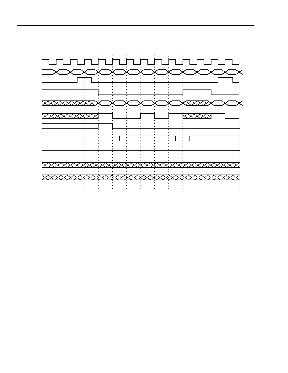
148
Agere Systems
Preliminary Data Sheet
August 2001
T1/E1/J1/J2 ATM Processor
TAAD08JU2 Newport
17 ATM Adaption Layer (AAL) Block
(continued)
1605 (F)
Figure 60. Packet Transmission on the SIF Interface with the PHY Stalling
0000
0001
0002
0003
0004
0005
0006
0007
04
1F
03
1F
02
1F
01
1F
01
1F
00
1F
00
1F
TxClk
TxAddr
TxPPA
TxEnb
TxData
TxPrty
TxSOP
TxSPA
TxEOP
TxErr
TxSize

Agere Systems
149
Preliminary Data Sheet
August 2001
T1/E1/J1/J2 ATM Processor
TAAD08JU2 Newport
17 ATM Adaption Layer (AAL) Block
(continued)
1606 (F)
Figure 61. Packet Transmission on the SIF Interface with the Master Stalling
04
1F
00
1F
03
1F
02
1F
01
1F
00
1F
00
1F
0004
0003
0002
0001
0000
0006
0005
TxClk
TxAddr
TxPPA
TxEnb
TxData
TxPrty
TxSOP
TxSPA
TxEOP
TxErr
TxSize

150
Agere Systems
Preliminary Data Sheet
August 2001
T1/E1/J1/J2 ATM Processor
TAAD08JU2 Newport
17 ATM Adaption Layer (AAL) Block
(continued)
1607 (F)
Figure 62. Reception of a Cell on the SIF Interface
R
X
SOP
R
X
Data
R
X
Enb
R
X
PPA
R
X
Addr
R
X
Clk
R
X
Prty
0003
1F
02
1F
01
1F
00
1F
00
1F
0000
0001
0002
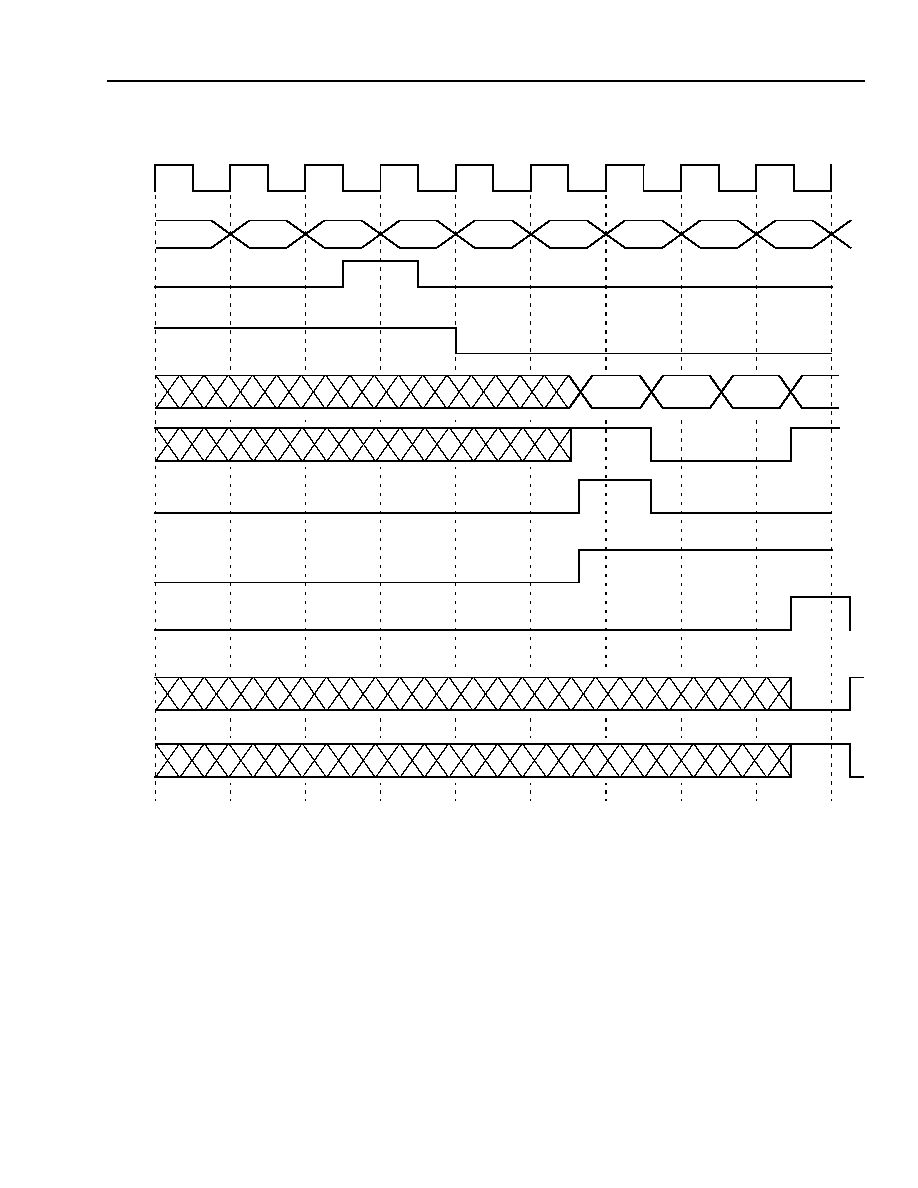
Agere Systems
151
Preliminary Data Sheet
August 2001
T1/E1/J1/J2 ATM Processor
TAAD08JU2 Newport
17 ATM Adaption Layer (AAL) Block
(continued)
1608 (F)
Figure 63. Reception of a Packet on the SIF Interface with No Stalls
R
X
SOP
R
X
Data
R
X
Enb
R
X
PPA
R
X
Addr
R
X
Clk
R
X
Prty
0003
1F
02
1F
01
1F
00
1F
00
1F
0000
0001
0002
R
X
Val
R
X
EOP
R
X
Err
R
X
Size

152
Agere Systems
Preliminary Data Sheet
August 2001
T1/E1/J1/J2 ATM Processor
TAAD08JU2 Newport
17 ATM Adaption Layer (AAL) Block
(continued)
1639 (F)
Figure 64. Reception of a Packet on the SIF Interface with the PHY Stalling
05
1F
04
1F
03
1F
02
1F
01
1F
00
1F
00
1F
RxClk
RxAddr
RxPPA
RxEnb
RxData
RxPrty
RxSOP
RxVal
RxEOP
RxErr
RxSize
0001
0000
0002
0003
0004
0005
0006

Agere Systems
153
Preliminary Data Sheet
August 2001
T1/E1/J1/J2 ATM Processor
TAAD08JU2 Newport
17 ATM Adaption Layer (AAL) Block
(continued)
1640 (F)
Figure 65. Reception of a Packet on the SIF Interface with the Master Stalling
17.7.2 Polling Algorithms For UTOPIA 2 and UT2+ Modes
17.7.2.1 Receive Interface Polling
The polling sequence is governed by the following rules:
!
It starts at MPHY address the minimum address configured after being enabled.
!
It increments the PHY address by one for each successive poll.
!
After reaching the maximum configured address, it wraps back to the minimum. These first three rules define the
basic PHY address polling sequence.
!
After reaching the maximum configured address, it wraps back to the minimum. These first three rules define the
basic PHY address polling sequence. When the cell/packet available signal is detected in response to a poll, the
SIF polls one more PHY address and suspends polling. The response to the second polled address is ignored.
Immediately after the first PHY address is selected, polling resumes. The next poll address will be the PHY
address which was ignored.
!
In UTOPIA 2 mode, it skips the active PHY address without delay during the first 27 cycles (53 cycles in 8-bit
mode) of a cell transfer (RXEN asserted). In UT2+ mode, it skips the active PHY address without delay until
EOP is received from the active PHY device.
04
1F
03
1F
00
1F
02
1F
01
1F
00
1F
00
1F
RxClk
RxAddr
RxPPA
RxEnb
RxData
RxPrty
RxSOP
RxVal
RxEOP
RxErr
RxSize
0001
0000
0002
0003
0004
0005

154
Agere Systems
Preliminary Data Sheet
August 2001
T1/E1/J1/J2 ATM Processor
TAAD08JU2 Newport
17 ATM Adaption Layer (AAL) Block
(continued)
!
If, after the 27th cycle (53rd cycle in 8-bit mode) of a cell transfer in UTOPIA 2 mode or after EOP is detected in
UT2+ mode, the round-robin PHY address is not the (previously) active PHY address and polling is not stopped,
it preempts the round-robin sequence for one poll slot, and polls the (previously) active PHY address. After pre-
emption, the next poll address will be the PHY address that was preempted. Each device should indicate its sta-
tus by asserting the RXPPA signal low (no packets/cells to transfer) or high (packets/cells available) after
sampling its address on RXADRR.
A receive cell transfer occurs when the following conditions are all met:
!
A physical device is detected with a packet/cell available.
!
A transfer is not currently active.
!
There is space in the internal FIFO for a new cell.
Cell transfers occur as soon as the transfer conditions are met. The SIF selects the device by placing the device
address on the address bus RXADRR, and subsequently bringing down the receive enable signal RXEN. Selection
preempts the polling sequence if it is active.
In UTOPIA 2 mode, the SIF then reads 27 words (53 words in 8-bit mode) without pausing, starting from when the
receive start of cell/packet signal is asserted. The transfer proceeds in open-loop fashion until all the words are
read. In UT2+ mode, the SIF reads words from the selected PHY, pausing if the slave deasserts RXVal, until EOP
is received from the slave.
17.7.2.2 Transmit Interface Polling
The polling sequence is governed by the following rules:
!
It starts at the minimum configured PHY address after being enabled.
!
It increments the PHY address by one for each successive poll.
!
After reaching the maximum configured PHY address it wraps back to the minimum. These first three rules
define the basic PHY address polling sequence.
!
In UTOPIA 2 mode, it skips the active PHY address (without delay) during the first N Ł 4 cycles (N is 27 and 53
for 16-bit mode and 8-bit mode, respectively) of a cell transfer (TXEN asserted). In UT2+ mode, it skips the
active PHY address (without delay) until it sends out an EOP.
!
If, after the N Ł 3 cycle of a cell transfer in UTOPIA 2 mode or EOP assertion in UT2+ mode, the round-robin
PHY address is not the active PHY address, it preempts the round-robin sequence for one poll slot, and polls the
active PHY address. After preemption, the next poll address will be the PHY address that was preempted.
Each device should indicate its status by asserting the TXPPA signal low (no packets/cells to transfer) or high
(packets/cells available) after sampling its address on the transmit address bus TXADRR. If the device responds
with packet/cell available asserted, the SIF then transmits to it 27 or 53 words (corresponding to 16-bit mode and
8-bit mode), without pausing in UTOPIA 2 mode. In UT2+ mode, it transmits words, pausing for the slaves asser-
tion of TXSPA, until EOP assertion. The SIF asserts the transmit start of cell signal only for the duration of the first
word being transmitted.
If an MPHY unexpectedly changes status after being polled (for instance, if it responds it is available when polled
but unavailable when selected), then the SIF sets a status bit indicating a protocol error but continues to send a
complete packet/cell.

Agere Systems
155
Preliminary Data Sheet
August 2001
T1/E1/J1/J2 ATM Processor
TAAD08JU2 Newport
17 ATM Adaption Layer (AAL) Block
(continued)
17.7.3 NIF
The NIF UTOPIA 2 interface is fully compliant with ATM Forum Technical Committee, UTOPIA Level 2, Version
1.0, af-phy-039.000.. NIF implements up to four Tx slave PHYs and a single Rx slave PHY. NIF is a 16-bit device
only; 8-bit mode is not supported. NIF implements cell level handshaking only; octet level handshaking is not sup-
ported. Configuration of the NIF is done via commands described in Sections 21.5.7 through 21.5.9.
17.7.4 ESI
Figure 66 shows the functional timing diagram for message reporting on the ESI. The beginning of the message is
marked by a synchronization pulse RESYNC. Message data REDATA[16:0] arrives on three consecutive clock
cycles. Output RECLK is produced so that RESYNC and REDATA may be captured by an off-chip message gath-
erer on the positive edge of RECLK with plenty of setup time. RECLK is runs at the same frequency as the GCLK
pin, but is not phase-aligned with GLCK.
1656 (F)
Figure 66. ESI Functional Timing Diagram
RECLK
REDATA
RESYNC
MESSAGE-A
MESSAGE-A
WORD 1
MESSAGE-A
WORD 2
MESSAGE-B
WORD 0
MESSAGE-B
WORD 1
MESSAGE-B
WORD 2
MESSAGE-C
WORD 0
MESSAGE-C
WORD 1
MESSAGE-C
WORD 2
WORD 0

156
Agere Systems
Preliminary Data Sheet
August 2001
T1/E1/J1/J2 ATM Processor
TAAD08JU2 Newport
18 Firmware Flows
Because Newport represents a true system-on-chip implementation, a mechanism is provided to simplify OAM
through an API abstraction that uses high-level command/responses rather than register level transactions. Thus,
Newport realizes a value proposition that simplifies provisioning by presenting high-level control capabilities to the
external host that encapsulate low-level control transactions within the device. An on-chip processor is used to pro-
vide this device-level OAM abstraction function.
Similarly, fault management is unified through the correlation of fault detection and isolation without requiring much
intervention from the external host. The device enables overall faster response to anomalous conditions, resulting
in less data loss.
The following sections describe the requirements and objectives for Newport's software architecture.
18.1 Software Architecture Overview
A high-level view of the software architecture is presented in Figure 67.
0008(F)
Figure 67. High-Level View of Software Architecture
APPLICATON
SNMP
BAPI: BOARD LEVEL API COMPONENT
GUI
(PLATFORM DEPENDENT)
APPLICATON
LAPI: LOW LEVEL API COMPONENT
(PLATFORM INDEPENDENT)
DAPI: DEVICE API REGISTER ABSTRACTON
(DEVICE DEPENDENT)
MANAGED
DEVICE
(NEWPORT)
PHY
FRAMER
BLOCK
TC
ATM
AAL
SYSTEM
APC
SAR
INTERFACE
UNI
IMA

Agere Systems
157
Preliminary Data Sheet
August 2001
T1/E1/J1/J2 ATM Processor
TAAD08JU2 Newport
18 Firmware Flows
(continued)
A set of APIs manages a suite of Agere devices by providing the capability to hide register details and device-spe-
cific procedures. The LAPI abstracts the target device (Newport) into a set of managed objects. The BAPI imple-
ments a set of functions specific to the device and allocates resources for the LAPI. The BAPI also provides
hardware interrupt services for the LAPI.
Because of hardware abstraction, no assumptions need be made about the underlying hardware. The application
indicates device type and memory location, allowing multiple devices to be supported simultaneously. Functions,
ports, and connections are encapsulated as objects which are accessed via handles.
The embedded device controller (which resides in software executed in the external board host processor) pro-
vides built-in protection (such as ISRs, control, alarms, and audits) for multitasking RTOSs (including pSOS,
VxWorks). The embedded device controller supports debugging via scripting for LAPI function calls and
register I/O. The embedded device controller presents a clean, consistent interface (based on portable C) for all
Agere devices.
The device-level API implements the Newport-specific procedures necessary to abstract high-level functions from
low-level (internal) register accesses. The device-level API resides on an ARM940T on-chip processor.
The following provides a description of control plane functions that are provided within Newport for fault-detection
and isolation without requiring external management plan intervention.
18.2 Provisioning
This section describes the provisioning function support. Provisioning may be partitioned into the following tasks:
!
Device-level configuration
!
Port configuration (PHY-layer)
!
UNI/IMA link mapping (TC-layer)
!
ATM layer configuration
!
AAL engine configuration
The LAPI will offer support for group level and per-port provisioning.
18.2.1 PHY Layer Provisioning
This section describes the provisioning alternatives for the physical layer aspects of Newport. The following speci-
fies the PHY provisioning based on which device operation mode is configured (see previous section).
The physical ports represent virtual sub-PHYs to the main scheduler (which is implemented within the APC
macro). Moreover, reuse of the APC macro inherits certain aspects of that macro with regard to the UTOPIA
MPHY buses and how the internal busing works. For example, the APC macro supports two physical UTOPIA-2
MPHY buses (A and B). However, the current APC macro (v2) only supports a maximum of 31 sub-PHYs, which
may either be distributed between the two UTOPIA buses or only on a single UTOPIA bus. Finally, the APC macro
supports only 32 egress schedulers (one per sub-PHY port). With these constraints, Newport uses the internal
busing scheme shown in Figure 68.
In this manner, data movement is simple between the ATM layer (APC) and either the TC or AAL layers, using a
shared UTOPIA-2 MPHY A bus. Likewise, expansion or extension to external devices is possible via the UTOPIA-
2 MPHY B bus.

158
Agere Systems
Preliminary Data Sheet
August 2001
T1/E1/J1/J2 ATM Processor
TAAD08JU2 Newport
18 Firmware Flows
(continued)
0009(F)
Figure 68. Newport Internal Busing Scheme
The LAPI sends a command to assign any external devices to UTOPIA-B MPHY addresses as well as their egress
schedulers. The DAPI configures the device upon device-level provisioning for internal MPHY assignments (if any).
The user need only be aware of hard-wired MPHY assignments. The DAPI ensures that the user assignment and
device mode are correct. For example, if the user specifies internal framer mode via a command and then attempts
to enable MPHY 0-15 on UTOPIA Bus A of APC, an error is flagged (since the assignment is performed automati-
cally after selection of internal framer mode).
MPHY
AAL VPHY0
AAL VPHY1
AAL VPHY2
AAL VPHY3
HOST UTOPIA
HIGH-SPEED PHY/TC
EXT ALL1 SAR
EXT ALL1 SAR
EXT ALL1 SAR
APC BLOCK
UTOPIA-B
(POSSIBLE EXTERNAL
CONNECTIONS)
UTOPIA-A
(INTERNAL
CONNECTIONS ONLY)
HOST
4
5
7
24
25
26
27
31
UNI Link # 0
0
1
2
3
6
UNI Link # 1
UNI Link # 2
UNI Link # 3
UNI Link # 4
UNI Link # 5
UNI Link # 6
UNI Link # 7
NOTE: ANY UNI LINKS MAY REPRESENT
AN IMA GROUP, IN WHICH CASE
ANY LINKS BELONGING TO THAT
GROUP ARE NOT AVAILABLE AT
THIS INTERFACE
.

Agere Systems
159
Preliminary Data Sheet
August 2001
T1/E1/J1/J2 ATM Processor
TAAD08JU2 Newport
18 Firmware Flows
(continued)
PHY layer provisioning includes:
!
Framing mode: T1 SF, T1 ESF, E1 (E-bit or no E-bit), J1, or J2 (NTT or TTC/ATM Forum)
!
Line code: B8ZS, CMI, HD3B, or AMI
!
UNI vs. IMA link type
!
Fractional ATM logical channel size: TDM logical channel size (per link)
!
Synchronization reference (external master or loop-timed)
The DAPI checks for consistency across link assignments to prevent incorrect provisioning (such as T1 + CMI or
E1 + ATM logical channel assigned to TS0 or 16).
0010(F)
Figure 69. PHY Layer Provisioning
18.2.2 Link Provisioning
The LAPI offers two types of PHY provisioning services, one based on individual links and one based on groups of
links (e.g., IMA groups). In the first case, individual links are provisioned individually (as above). In the second
case, links are provisioned implicitly through group provisioning. Thus, within an IMA group, all links are provi-
sioned with four common link parameters:
!
Assign n of 31 links to group m:
-- Mutually exclusive.
-- Links are addressed by the IMA group round-robin according to the ordinal order of their MPHY address
-- The MPHY address of a link is implicitly the bit number of the link assignment vector.
-- Links within a group need not be consecutive, but are still added to the round-robin based on ascending order
of MPHY address.
-- Need MIB mapping to MPHY for particular IMA group.
!
Parameters for ProvisionIMAGroup command are as follows:
-- Speed and framing mode
-- IMA frame size
-- IMA frame offset
-- ICP soft parameters
!
ICP-specific parameters (per group)
!
Test link option (parameters)
In the case of external framer mode, the UTOPIA-2 bus is used for all line-side ingress/egress data flow. The fol-
lowing command/parameters are applicable to this mode:
!
Bus speed
!
Active subports (MPHYs)
ATM LOGICAL CHANNEL
TDM LOGICAL CHANNEL
0
n
n+1
BW ALLOCATED TO
TC/ATM/AAL FUNCTION
BW ALLOCATED TO
EXTERNAL TDM FUNCTION

160
Agere Systems
Preliminary Data Sheet
August 2001
T1/E1/J1/J2 ATM Processor
TAAD08JU2 Newport
18 Firmware Flows
(continued)
Table 36 illustrates how physical link assignments are made for IMA groups. Newport provides four 32-bit IMA link
assignment registers (one for each group). Each bit corresponds to an implemented of potential physical link. Only
the eight-LSBs are valid, corresponding to links terminated directly by Newport. Bits 8 through 31 are reserved for
future implementation of larger IMA groups through an IMA expansion mode.
To assign a link to an IMA group, set the bit corresponding to the link in the IMA group's link assignment register.
Once a particular group has made a link assignment, no other group can use that link. The device manager checks
the configuration and flags an error if such an attempt is made. A zero in any particular bit position indicates that
the corresponding link is not assigned to that group.
Links are added to the round-robin in order of increasing integer value. Links need not be consecutive.
Table 37. Link Assignment Register Set for IMA Group N
In this particular case, incoming cells for this IMA group N are distributed across links 1, 2, and 5 in the following
order:
1, 2, 5, 1, 2, 5, 1, 2, 5, . . .
Now, consider a second link assignment register for IMA group M (Table 38).
Table 38. Link Assignment Register Set for IMA Group M
The order of the round-robin sequencing for IMA M is as follows:
0, 3, 4, 6, 7, 0, 3, 4, 6, 7, . . .
If desired, the link ID may be derived from this link assignment register set.
Table 36. Link Assignments for IMA Groups
B
31
B
30
B
29
B
28
B
27
B
26
B
25
B
24
B
23
B
22
B
21
B
20
B
19
B
18
B
17
B
16
B
15
B
14
B
13
B
12
B
11
B
10
B
9
B
8
B
7
B
6
B
5
B
4
B
3
B
2
B
1
B0
IMA
GROUP
0
0
0
0
0
0
0
0
0
0
0
0
0
0
0
0
0
0
0
0
0
0
0
0
0
0
0
0
1
1
1
1
IMA
GROUP
1
0
0
0
0
0
0
0
0
0
0
0
0
0
0
0
0
0
0
0
0
0
0
0
0
0
1
1
0
0
0
0
IMA
GROUP
2
0
0
0
0
0
0
0
0
0
0
0
0
0
0
0
0
0
0
0
0
0
1
1
1
0
0
0
0
0
0
0
IMA
GROUP
3
0
0
0
0
0
0
0
0
0
0
0
0
0
1
1
1
1
1
1
1
1
0
0
0
0
0
0
0
0
0
0
B7
B6
B5
B4
B3
B2
B1
B0
0
0
1
0
0
1
1
0
B7
B6
B5
B4
B3
B2
B1
B0
IMA Group N
0
0
1
0
0
1
1
0
IMA Group M
1
1
0
1
1
0
0
1

Agere Systems
161
Preliminary Data Sheet
August 2001
T1/E1/J1/J2 ATM Processor
TAAD08JU2 Newport
18 Firmware Flows
(continued)
18.2.3 Connection Provisioning
Connection provisioning refers to connection table setup (rather than connection establishment). In this case, the
shared buffer memory may be partitioned according to the type of traffic expected (80% voice, 20% data, etc.) for
more efficient operation, as follows:
!
Provision buffer segment size (10 octets for voice, 64 octets for data)
!
Provision VP switching and VC termination (PVC mode)
18.2.4 AAL2 Provisioning
The following global parameters must be provided:
!
Total number of CIDs per VC
!
Max-length-SDU
18.2.5 System Interface Provisioning
System interface provisioning is performed to configure the operation mode for the particular system interface type
used. Options include the following:
!
UTOPIA MPHY cell bus (1 port, 32 subports)
!
UTOPIA MPHY packet bus (1 port, 32 subports)
L2 addressing format must also be provisioned (length/format of fields).
!
UTOPIA packet bus: max packet length
18.3 Operation
This subsection describes device manager interaction for operation of the device. For the purposes of this descrip-
tion, operation refers to those aspects for connection management, including connection setup, monitoring, and
tear-down.
The following types of connections are managed through the device manager interface:
!
VPCs (for VP switching)
!
VCCs (for VC termination of AAL2 and AAL5 flows)
!
AAL2/LLCs (for AAL2 connection setup)

162
Agere Systems
Preliminary Data Sheet
August 2001
T1/E1/J1/J2 ATM Processor
TAAD08JU2 Newport
18 Firmware Flows
(continued)
VPC connections are used for add/drop multiplexer pass-through flow management. In the case of a daisy-chain
network, certain connections may be terminated (as VCCs) by a node or passed through to a subsequent or previ-
ous node (as VPCs). The assumption is that such flows are distinguished as VPC flows. This enables rapid switch-
ing/rescheduling of cell flows within a node as well as control of queueing to minimize intermediate node queue
build-up to provide latency bounds on flows within the daisy-chain network.
VCC connections are used for cell flows which are terminated by a particular node (or Newport device). In these
cases, a VCC may correspond to different classes such as multiple AAL5 connections, each VBR or ABR with dif-
fering traffic parameters or AAL2 VCs. By proper scheduling and buffer management, Newport provides service
guarantees to a broad range of VCC connection classes, traffic types, and priorities.
Finally, a VCC may correspond to an AAL2 cell flow which encapsulates LLCs that correspond to different classes,
such as compressed speech, asynchronous data, or real-time video (via I.366.1/I.366.2 transport control).
A node may be configured to terminated VPCs from a range of VPIs and VCCs from a range of VCCs within a VPI.
Cell filtering of cell headers is provided to rapidly associate a particular cell with known connections for routing/ter-
mination.
Provisioning per port:
!
VPI/VCI ranges
Provisioning per VPC:
!
Destination port
!
Priority/class
!
Traffic parameters
Provisioning per VCC:
!
Destination port
!
AAL type
!
Priority/class
!
Traffic parameters
Provisioning per LLC:
!
Destination port. This assumes we are providing reassembly service to AAL2 LLCs for a host (rather than for-
ward cell to it).
!
AAL type
!
Priority/class
!
Traffic parameters
Description should include how to specify GCRA parameters (related to traffic parameters and priority assign-
ment).
Description should also include LLC-XC (loopback mode) parameters:
!
Egress port (PHY level)
!
Egress VCI/VPI
!
Egress LLC
!
Priority/class
Will inherit several APC functions here related to scheduling, buffer management, etc.

Agere Systems
163
Preliminary Data Sheet
August 2001
T1/E1/J1/J2 ATM Processor
TAAD08JU2 Newport
18 Firmware Flows
(continued)
18.3.1 Management Plane Interaction via External Host
In order to enable the external host to interact with the AAL engine for insertion/extraction of AAL2 peer end-to-end
communications, Newport provides the following primitives:
!
MAAL-UNITDATA.request: used to deliver data from the management plane to the CPS transmitter.
!
MAAL-UNITDATA.indication: used to deliver data from the CPS receiver to the management plane.
In either case, Newport provides a mailbox type of interface. In particular, Newport will provide SS-SAR CPS ser-
vices for the external host device for relaying these messages. In the send (transmit) direction, Newport associates
the packet with a particular class-of-service (within the AAL engine), segments the packet into CPS-SDUs, and
multiplexes the CPS-SDUs into the ATM SDU.
In the receive direction, Newport associates the AAL2 connection (CID) with the host device, reassembles multiple
CPS_SDUs into an AAL-SDU, verifies the packet (if applicable), and forwards the packet to a dedicated buffer for
retrieval by the host device.
This capability only applies to line-side communications. For example, in the case of APC/fabric mode, there is no
need to send AAL2 management layer messages across the fabric. AAL2 peer communication implies communi-
cation across CPS users (i.e., toward the line interface). A separate cell-level insertion/extraction capability will be
provided for host communication across the fabric (via the APC's own cell capture/insert).
The format for the host to AAL engine capability is as follows:
CPS-INFO: Specifies the interface data unit exchanged between the CPS and layer management. The interface
data is an integral multiple of one octet (1:45 or 1:64).
CPS-UUI: Parameter transparently transported by the CPS between peer layer management entities (5 bits, only
values 30 and 31 are permitted).
CPS-CID: Parameter contains a channel identifier (CID) which identifies the CPS connection for which this man-
agement information is exchanged (8-bits).
Note: I.363.2 implies that this technique may be used to exchange information about a particular CID such that the
layer management sends CAS whereby the CID may correspond to the CID used by an SSCS entity, but the
UUI identifies the CPS-SDU as a signaling type so that the payload is understood by the layer management
application. This is in contrast to using a CSC-type AAL2 connection whereby the CID identifies a connec-
tion that is shared across many connections and the internal protocol identifies the particular connection to
which a control message pertains. The implementation should allow either technique to be used. In the case
of the CAS approach, the inserted packet will pertain only to the egress direction (and will not be relayed to
the SSCS entity). In the case of the ingress direction, the UUI field will be filtered and all CPS-SDUs with
UUI values of 30 or 31 will automatically be directed toward the host interface.
18.3.2 Provisioning of AAL2 Connection
To accommodate an AAL2 CPS user, the following tasks must be provided. (an AAL2 CPS user may be control or
data):
1. First, an AAL2 connection must be established. This requires opening a VC on a particular logical PHY and
relating it to an AAL Type 2 connection.
2. A VPI/VCI assignment must be made, along with a scheduling priority assignment. Subsequent CPS users of
that AAL2 connection may be opened in either a PVC or SVC fashion.
3. A PVC may be established for any number of AAL2 CPS connections by providing context descriptors and
enabling the channel for peer-to-peer CPS user communication.
The connection descriptor enables the CPS-SDU to be routed to the correct SSCS destination, whether by cell or
packet protocol.

164
Agere Systems
Preliminary Data Sheet
August 2001
T1/E1/J1/J2 ATM Processor
TAAD08JU2 Newport
18 Firmware Flows
(continued)
18.4 Alarm Generation and Reporting
This subsection describes the anomaly/defect detection and alarm generation capabilities of Newport.
In recognition of Newport's system-on-a-chip architecture, the DAPI simplifies device interaction through services
provided by the ARM processor. The advantages of this interface design extend to the areas of alarm processing
where fault detection, persistence, and isolation are provided automatically by the device with minimal interaction
required by the external host processor.
The key requirement of this alarm processing feature is to perform alarm correlation in order to relate failure states
to the corresponding actions minimizing service interruption. Correlation refers to the following actions:
!
Receiving failure indications from multiple sources (as anomalies propagate through the system).
!
Relating the indications to a particular error event.
!
Processing the alarms to perform the required mitigation of the defect.
!
Providing the proper indication to the external host processor/L-API for further (higher-level) actions.
In analogy with the introductory logical view of Newport's ATM structure, alarm processing should be viewed in
relation to how errors propagate through each level, how they are detected, how they are reported, and how they
may be mitigated.
Figure 70 illustrates the scenario of a link failure in an IMA group. The circled numbers refer to error indications
provided from each logical block to the D-API. The subgroup describes errors that may be indicated in sequence
as a result of the initial failed link. For example, (A1) refers to the error indications from the PHY (framer) block.

Agere Systems
165
Preliminary Data Sheet
August 2001
T1/E1/J1/J2 ATM Processor
TAAD08JU2 Newport
18 Firmware Flows
(continued)
0011(F)
Figure 70. IMA Group Link Failure
As a result of the failed link, the first event detected by Newport is an LOS for that port, followed by LOF, and
LOMF after successive integration intervals of the anomalous condition. In response to the LOS, the DAPI will
send an External_AIS_Alarm packet downstream (toward the system interface) for each AAL2 CID on that original
PHY port. This packet will be sent once per second until the fault clears. In response, the DAPI will send an RAI
indication in the upstream direction on that PHY.
The second event detected by Newport is an LOCD for that port that is detected by the TC block. In response to
the LOCD, the TC cell delineation state machine will transition into a search state, searching for a new cell delinea-
tion sequence.
The third event detected by Newport is an LIFS for that link, detected by the IMA block. In response to the LIFS,
the IMA frame delineation state machine will transition into a search state. In further response, the IMA GSM will
remove the link from the round-robin (transitioning through the appropriate indications on the transmit link LSM)
and apply backpressure to the ATM layer to indicate a smaller virtual link capacity. The transmit GSM will redistrib-
ute the load across all remaining good links within the IMA group
.
No errored cells should have been passed beyond the TC layer. Similarly, fault indication will be handled via DAPI
interaction with AAL engine.
PHY
TC
IMA
ATM
SYS
I/F
AAL
A1
D-API
HOST BUS
L-API
A2
A3
A4
A5
A6
A1
1. LOS
2. LOF
3. LOMF
4. LOCD
5. LIFS
6. L-VP CONN
7. L-VC CONN
8. L-ABR
9. L-F4/F5
A2
A3
A4

166
Agere Systems
Preliminary Data Sheet
August 2001
T1/E1/J1/J2 ATM Processor
TAAD08JU2 Newport
18 Firmware Flows
(continued)
By comparison with less integrated solutions, the alarm indications would require detection, processing, and corre-
lation by an external host processor. Subsequent intervention between the host and multiple devices would be
needed to react to the fault. Data loss and service interruption would occur as a result of a nonintegrated architec-
ture. While these side effects may not be as apparent in low-speed access applications, the overall cost and devel-
opment time incurred by a multivendor, multidevice solution represent a highly intangible cost.
The remainder of this subsection describes more completely the types of errors detected within the device and the
capabilities for controlling device operation to mitigate the errors.
18.4.1 Layer 1 (PHY)
!
Loss of signal (LOS)
!
Loss of frame (LOF)
!
Loss of multiframe (LOMF)
!
Remote alarm indication (RAI)
!
Alarm indication signal (AIS)
!
G.704, G.732, G.733, G.735, G.775, T1.231, and TR-NWT-000170
18.4.2 ATMF Specifications
!
LOS, LOF, and AIS. Send external AIS alarm packet downstream on each AAL type 2 connection assigned to a
VC on the failed narrowband interface. Repeat once per second on each connection until the fault clears. Alarm
packets are not sent in a channel used for signaling.
!
RAI. Send RAI in upstream direction. Upon detection of RAI, send external RAI alarm packet downstream on
each AAL2 connection. Repeat once per second until fault clears. No alarm packets are sent on signaling chan-
nels.
!
Upon detection of LOMF (E1/CAS), send an external AIS alarm packet downstream on each AAL2 connection.
Repeat once every second until fault clears. Send MFRAI in upstream direction.
!
When receiving external AIS alarm packet for AAL2 CID, transmit xFF on connected E1 channel until no external
AIS alarm packet is received for 3.5 seconds or until receipt of valid user data from other end.
!
When receiving external AIS alarm packet for AAL2 CID, apply trunk conditioning on DS1 downstream per TR-
NWT-000170, Issue 2 until no external AIS packet is received for 3.5 s or until receipt of valid user data from
other end.
!
A bit in TS0 will be used for RAI. It is set to 0 for no remote alarm indication and to 1 for RAI.
!
The CRC-4 bits are used for multiframe alignment per G.704 [2.3.3] and G.706. The E bits are used to provide
an indication of LOMF. The E bits should optionally be set to 1 if equipment does not support them.
!
Sa bits G.704, section 2.3.2 Table 4a.
!
J2/ATMF 6.312 Mbits/s UNI (not based on DS2).
!
LOS per 6.1/I.432, detection/removal per G.775.

Agere Systems
167
Preliminary Data Sheet
August 2001
T1/E1/J1/J2 ATM Processor
TAAD08JU2 Newport
18 Firmware Flows
(continued)
18.4.3 E1/ATMF
!
LOF detected when 7 or more consecutive errored framing patterns (4 multiframes) are received. LOF cleared
when 3 or more consecutive correct framing patterns are received. The framing bit is carried in the last 5 bits of
a frame (following 98 time slots). The framing pattern is b110010100. If one or more bits are erroneous during a
particular multiframe, only a single errored frame is counted.
!
AIS. Sent from NT1 to user to indicate loss of 6.312 Mbits/s frame on the network side. AIS is defined as a bit
array of 6.312 Mbits/s with all bits set to 1. Detection and removal of AIS per G.775.
!
Payload AIS. sent from the network to the user to indicate loss of transmission capability of 6.312 Mbits/s pay-
load [TS1-TS96]. Payload-AIS defined as a bit array of the frame payload where all bits are set to 1. Detected at
user side when the incoming signal [TS1-TS96] has 2 or less 0s in a sequence of 3072 bits (0.5 ms). Payload-
AIS is cleared when the incoming signal [TS1-TS96] has 3 or more 0s in a sequence of 3072 bits (0.5 ms).
!
RAI indicates loss of PL capability at the UNI (LOF, LOS and/or AIS). When detected at user side, generate RAI
and transmit to the network side. RAI is defined on m-bits as a repetition of the 16-bit sequence consisting of
eight binary 1s and eight binary 0s in m-bits. When RAI signal is not sent (i.e., normal operation), the HDLC flag
pattern (x7E) is sent in the m-bit. RAI is detected when 16 or more consecutive RAI-patterns are received. The
RAI is cleared when four or more consecutive incorrect-RAI-patterns are received.
18.4.4 Layer 2 (TC)
!
I.432.
!
LOCD failure per 6.1/I.432. Detection/removal per I.432/6.1.
!
IMA Specification. If the IDCR is decreased due to a loss of a transmission link (as opposed to a maintenance
layer link deletion), the action must be detected and some VCs may be dropped so as to ensure delay and cell-
loss-ratios of certain (important) connections. Presumably, the ATM layer (APC) schedules traffic according to
the aggregate virtual link rate
.
If the IDCR is decreased due to administration, the control plane should ensure
that the remaining connections will still achieve their contract. This requires close interaction with the CAC and
management plane.
!
LODS. Detect based on receive differential delay measurement. If exceeded, assert alarm to ARM, return indi-
cation to FE (via ICP) and cycle transmit link through state.
!
LIFS. Detect based on ICP checking (HEC and offset).
!
Several parameter failures detected and alerted to ARM for IMA (unsupported parameter, unsupported clock
mode, etc.).
!
Detection of a persistent defect (AIS | LOCD | LIFS | LODS) by receiver should cycle to Rx_Failed. [Cycle to Rx-
Unusable/Monitor (failed or fault).] Forward Rx state to GSM for encoding in Tx ICP link information field (within
2M cells on the link); set SCCI field for the first ICP cell to reflect a change.
!
GSM: indication of time-out (config-abort to start-up transition).
!
GSM: transition to insufficient links if necessary.
!
TC (HUNT, SYNC, PRESYNC (per-link Rx)).

168
Agere Systems
Preliminary Data Sheet
August 2001
T1/E1/J1/J2 ATM Processor
TAAD08JU2 Newport
18 Firmware Flows
(continued)
!
LOC Indication. Inconsistent provisioning: disallowed number of links and groups, link(s) assigned to multiple
groups, J2 mode link, and link assigned to IMA group (only support T1/E1/J1 in IMA mode).
!
Detection of idle cells while in IMA mode.
!
Not configured: The group does not exist.
!
Start-up: This end is in start-up and is waiting to see the FE in start-up. After sufficient communication with the
FE has been achieved, the group parameters (M, symmetry) are recorded and the group moves to Start-up-Ack.
!
Start-up-Ack: A transitional state used during start-up; FE indications are ignored while in this state.
!
Config-aborted: This state is entered when the FE tries to use unacceptable configuration parameters.
!
Insufficient-Links: This state implies that the NE does not have a sufficient number of links in the active state,
either active in the Tx or Rx direction.
!
Blocked: The group is blocked (e.g., for testing or maintenance) while sufficient links are active in both directions.
!
Operational: The group is not inhibited and has sufficient links in both the Tx and Rx directions. The IMA is now
capable of transmitting and receiving ATM layer cells.
18.4.5 Layer 3 (ATM)
!
I.432.
!
F5 OAM (to detect ATM VCC connectivity failures per I.610).
!
E1 CCS. In case of loss of ATM connectivity, transmit xFF on signaling channel of DS1 until condition clears.
Transmit xFF on all user data channels until the condition clears.
!
DS1 CCS. In case of loss of ATM connectivity, transmit trunk conditioning per TR-170 on signalling channel until
condition clears. Transmit trunk conditioning on user data channels until the condition clears.
!
Switched Interface.: In case of switched connections, apply time-outs to any active connection and disconnect
after the time-out. All new calls to that interface will be blocked (LOS, LOF, or AIS). The same applies to loss of
ATM connectivity: release calls after time-out (must allow sufficient time for protection switch to occur prior to
releasing calls).
!
When RAI is detected, block new call setups to that interface.
!
J2/6.312 Mbits/s: VP-RDI signal (3.5.3.1) is used to indicate the LOS, LOF, LODC, AIS, and Payload-AIS failure
indications to upstream equipment (ATMF specification, ATM layer).
18.4.6 Layer 4 (AAL)
!
No AAL2 connectivity fault detection method specified. May be due to LOS or LCD or through AIS/RDI/loopback
or F5 cells.
!
Device/physical (buffer management, etc.).

Agere Systems
169
Preliminary Data Sheet
August 2001
T1/E1/J1/J2 ATM Processor
TAAD08JU2 Newport
19 Embedded Device Controller (EDC) Firmware
This document describes the ARM or embedded device controller (EDC) software running on Newport. It provides
the interface for the world outside the Newport chip to interact with the chip. The goal of the embedded processor
on Newport is to minimize the interaction between Newport and an external host (ExH). This is achieved in part by
defining various modes of Newport and embedding the initial configuration of the device in the ARM code. This
means that via the download code command the ExH provides the ARM its run time code and the mode. Within in
this run time code is the initial configuration. Once the ARM completes the initial configuration, the only provision-
ing the ExH needs to do is for individual connections.
The initial modes of Newport are defined in Table 39.
Table 39. Newport Operating Modes
Mode
Description
Internal PHY
Normal mode where all Newport blocks are being used.
APC-W
Backward-compatibility mode where only the APC is used.
Newport has look and feel of stand-alone APC.
External PHY
Newport PHY layer blocks are not used; external data is passed directly to ATM/AAL layers.
AAL Slave
Newport acts as a stand-alone AAL engine.

170
Agere Systems
Preliminary Data Sheet
August 2001
T1/E1/J1/J2 ATM Processor
TAAD08JU2 Newport
19 Embedded Device Controller (EDC) Firmware
(continued)
19.1 Firmware Architecture
Figure 71 shows the relationship between the host processor, the EDC, and the hardware blocks.
0012(F)
Figure 71. ExH Processor, EDC, and Hardware Blocks
ONBOARD
EXH PROCESSOR
DEVICE MANAGER
OFF-BOARD NETWORK MANAGER
LOW-LEVEL API (LAPI)
COMMAND GENERATOR
INDICATION INTERPRETER
COMMANDS AND
INDICATIONS
INTERRUPT
NEWPORT
BUS MASTER
BUS SLAVE
INTERRUPT
CONTROLLER
PBUS
EDC
COMMAND INTERPRETER
SCHEDULER
BUS MASTER
BUS SLAVE
FIRMWARE MODULES
SUPER
FRAMER
TC/IMA
APC
AAL
ALARM
RATION-
ALIZATION
CODE
HOST
TO SRAM
CODE
API
API
TRANSFER
HARDWARE ABSTRACTION LAYER (HAL)
INITIALIZATION
CUSTOMER APPLICATION

Agere Systems
171
Preliminary Data Sheet
August 2001
T1/E1/J1/J2 ATM Processor
TAAD08JU2 Newport
19 Embedded Device Controller (EDC) Firmware
(continued)
19.2 Reset and Booting
Since there is always an ExH present in a Newport system, the ARM remains in reset even after the reset signal is
deasserted. It is the responsibility of the ExH to take the ARM out of reset. This is accomplished by writing a regis-
ter. For all Newport modes, the ExH downloads application code.
The ARM code is downloaded by the ExH via the EDCs command/data FIFO. The ExH writes the code segments
into the FIFO then writes the SRAM address for the ode segment into an EDC register. The EDC then writes the
data in the FIFO at the address specified. When the EDC empties the FIFO, it interrupts the ExH. The ExH can
then download the next segment until the whole binary image is downloaded into the SRAM.
19.3 Initialization
The initialization phase starts with the host using the address and control registers to take the ARM out of reset.
The ARM starts running the firmware in the SRAM. This brings the ARM into a state where it can process com-
mands from the host.
The host then sends the ARM a sequence of commands that set up Newport in the required mode. The user is
encouraged to use the Newport set-up utility, a GUI-based tool, to generate the sequence of set-up commands and
store them in a set-up file. The set-up utility allows the user to choose the mode setup information by simply click-
ing on the GUI to select options. It ensures that the user selects a valid combination of options by providing appro-
priate error messages and, where possible, by restricting the available options to the appropriate ones. This
methodology brings the great advantage that the EDC firmware is freed from having to perform error checking on
all the provisioning parameters, which reduces the embedded code size. In addition, the GUI handles the transla-
tion of Newport-wide provisioning parameters into per-block provisioning parameters, which also reduces the com-
plexity of the EDC initialization code.
Once the host has downloaded the set-up file to Newport, the provisioning of the Newport device is complete. The
ARM waits for the next command from the host or provides an indication to the host if an interrupt or an alarm goes
off in Newport.

172
Agere Systems Inc.
Preliminary Data Sheet
August 2001
T1/E1/J1/J2 ATM Processor
TAAD08JU2 Newport
20 Commands and Indications
The external host (ExH) communicates with the firmware using commands and indications. The host uses com-
mands to instruct the ARM (via the device manager) to perform its functions. Indications are used by the ARM to
inform the ExH of events that take place within the Newport chip. This section will describe the host programmer's
interface (HPI) for commands and indications.
The HPI is written from the point of view of the layers of the application. For Newport, this translates into com-
mands that configure the physical layer (the framer and the TC/IMA block), the ATM layer (APC block), and the
AAL layer (SAR block).
Commands and indications are processed through a combination of registers and buffers that are memory-
mapped on the ExH bus. When the ExH wants to send a command to Newport, it writes the command parameters
into the command data buffer and then writes the 32-bit command into the command register. The writing of the
command register causes an interrupt to the EDC. The EDC then reads the command and its parameters. When
the last parameter is read from the buffer, an interrupt is sent to the ExH notifying it that the command data buffer is
available. Indications are processed in the same way; just reverse the directions.
These buffers are also used to send and receive user-defined PRM messages, special ATM VCs, OAM cells (ATM
layer), or special AAL connections (SSCOP).
21 Commands
Commands are written to Newport in two steps: first, the command parameters are written, followed by the com-
mand. The arguments are written to an internal Newport buffer and then the command is written to a Newport reg-
ister. The act of writing this register causes an interrupt to the ARM. Commands have variable length and,
therefore, the size of the command data is contained in the command parameter. When the last word of the buffer
is read, an interrupt is sent to the ExH. This process implies that only one command is issued at a time.
21.1 Command Register Structure
Newport commands consist of a 32-bit command register and a series of parameters. The number of parameters is
variable and is limited to the size of the command buffer (256 x 32 bit words). The command register is defined in
Table 40.
Table 40. Fields of the Command Register
Bit(s)
Field Name
Description
1:0
CommandLayer The Newport layer to which the command is addressed:
00 = Global
01 = PHY
10 = ATM
11 = AAL
7:2
OpCode
A defined 6-bit number which identifies the command within its layer.
15:8
CommandTag
An 8-bit identifier to distinguish multiple outstanding commands of the same type.
26:16
CommandSize
The number of bytes in the commands data buffer is CommandSize, where Com-
mandSize is in the range 0 to 1024. Note that some commands don't take any
parameters, in which case this field is zero.
27
IndRequired
Specifies whether or not an indication of the command-complete type will be gen-
erated upon the completion of this command.
0 = Don't generate an indication.
1 = Generate an indication.
31:28
Reserved
Reserved.

Agere Systems Inc.
173
Preliminary Data Sheet
August 2001
T1/E1/J1/J2 ATM Processor
TAAD08JU2 Newport
21 Commands
(continued)
Table 41 provides a summary of all commands on the Newport device. The command type indicates the scope of
the command. Initialization and provisioning commands are used to configure the device before operation. Once it
has been set up, the ENABLE_PROCESSING command is issued to instruct the device to begin the processing of
data. Provisioning commands can also be used after the device has begun processing, as can dynamic reconfigu-
ration and signaling commands. Signaling commands deal with the flow of data through the device rather than its
configuration.
Table 41. Command List and Summary
Layer
OpCode
Command Name
Command Type
Reference
Global
1
NPT_CMD_ECHO
Diagnostic
page 176
2
NPT_GLBCLK_RATE
Initialization
page 176
3
NPT_ENABLE_PROCESSING
Initialization
page 176
PHY
0
NPT_PHY_CONFIG_GLOBALS
Initialization
page 177
1
NPT_PHY_CONFIG_LINK
Provisioning
page 184
2
NPT_PHY_ADD_LINK
Dynamic reconfiguration
page 191
3
NPT_PHY_DELETE_LINK
Dynamic reconfiguration
page 192
4
NPT_PHY_FRAMER_TEST_LINK
Dynamic reconfiguration
page 193
5
NPT_PHY_SEND_ALARMS
Signaling
page 194
6
NPT_PHY_FRAMER_LOOPBACK
Test
page 194
7
NPT_PHY_CHI_LOOPBACK
Test
page 195
8
NPT_PHY_IMA_CONFIG_GROUP
Dynamic reconfiguration
page 196
9
NPT_PHY_IMA_DELETE_GROUP
Provisioning
page 198
10
NPT_PHY_IMA_INHIBIT_LINK
Dynamic reconfiguration
page 198
11
NPT_PHY_IMA_INHIBIT_GROUP
Dynamic reconfiguration
page 198
12
NPT_PHY_IMA_TEST_LINK
Test
page 198
13
NPT_PHY_SET_STATS
Provisioning
page 198
14
NPT_PHY_SINGLE_STATS
Provisioning
page 199
15
NPT_PHY_GET_STATE
Query
page 199
16
NPT_PHY_READ_REG
Query
page 200
17
NPT_PHY_SET_LINK_ALARMS
Provisioning
page 200
18
NPT_PHY_SET_GROUP_ALARMS
Provisioning
page 202
19
NPT_PHY_FRAMER_BOM
Signaling
page 203
20
NPT_PHY_FRAMER_DL_THRESHOLDS
Provisioning
page 203
21
NPT_PHY_FRAMER_AUTOPRM
Provisioning
page 204
22
NPT_PHY_FRAMER_DATA_LINK_MSG
Data Link
page 205
23
NPT_PHY_FRAMER_FDL_STACK
Data Link
page 206

174
Agere Systems Inc.
Preliminary Data Sheet
August 2001
T1/E1/J1/J2 ATM Processor
TAAD08JU2 Newport
21 Commands
(continued)
ATM
0
NPT_ATM_INIT
Initialization
page 215
1
NPT_ATM_SCHED_INIT0
Initialization
page 221
2
NPT_ATM_SCHED_INIT1
Initialization
page 221
3
NPT_ATM_SCHED_INIT2
Initialization
page 221
4
NPT_ATM_SCHED_INIT3
Initialization
page 221
5
NPT_ATM_SCHED_CONFIG
Provisioning
page 222
6
NPT_ATM_SET_ALARM_MASK
Provisioning
page 224
7
NPT_ATM_SET_STATS_MASK
Provisioning
page 224
8
NPT_ATM_ADD_CONN
Dynamic reconfiguration
page 232
9
NPT_ATM_DELETE_UNI_CONN
Dynamic reconfiguration
page 238
10
NPT_ATM_DELETE_BI_CONN
Dynamic reconfiguration
page 239
11
NPT_ATM_SET_CONN_STATS
Dynamic reconfiguration
page 241
12
NPT_ATM_SET_CONN_FAULT_STATE
Dynamic reconfiguration
page 241
13
NPT_ATM_SET_CONN_OAM_CC
Dynamic reconfiguration
page 242
14
NPT_ATM_ENABLE_CONN_OAM_PM
Dynamic reconfiguration
page 243
15
NPT_ATM_DISABLE_CONN_OAM_PM
Dynamic reconfiguration
page 243
16
NPT_ATM_INSERT_CELLS
Signalling
page 244
17
NPT_ATM_GET_STATS
Query
page 245
18
NPT_ATM_READ_APC
Query
page 245
19
NPT_ATM_READ_DRAM
Query
page 246
AAL
0
NPT_AAL_FREE_LIST_ALLC
Initialization
page 259
1
NPT_AAL_NIF_TRANSMIT_CONFIG
Provisioning
page 259
2
NPT_AAL_NIF_RECEIVE_CONFIG
Provisioning
page 261
3
NPT_AAL_SIF_TRANSMIT_CONFIG
Provisioning
page 258
4
NPT_AAL_SIF_RECEIVE_CONFIG
Provisioning
page 259
5
NPT_AAL_ADD_CONN
Dynamic reconfiguration
page 266
6
NPT_AAL_ADD_CHANNEL
Dynamic reconfiguration
page 269
7
NPT_AAL_QUE_LEN_POL_TAB
Dynamic reconfiguration
page 262
8
NPT_AAL_CONN_QUE_LEN_POL
Dynamic reconfiguration
page 261
9
NPT_AAL_IL2_QUE_SHARE
Dynamic reconfiguration
page 262
10
NPT_AAL_IL2_QUE_PRIVATE
Dynamic reconfiguration
page 263
11
NPT_AAL_L1_QUE_QOS
Dynamic reconfiguration
page 264
12
NPT_AAL_IDU_SDU_TABLE
Dynamic reconfiguration
page 265
13
NPT_AAL_ENABLE
--
page 271
14
NPT_AAL_DELETE_CHANNEL
Dynamic reconfiguration
page 272
15
NPT_AAL_DELETE_CONN
Dynamic reconfiguration
page 272
16
NPT_AAL_SET_STAT_MODE
Dynamic reconfiguration
page 274
17
NPT_AAL_SET_CONNCHAN_STATS
Dynamic reconfiguration
page 274
18
NPT_AAL_ADD_STAT
Dynamic reconfiguration
page 274
19
NPT_AAL_FREE_STAT
Dynamic reconfiguration
page 278
20
NPT_AAL_GET_STAT
Dynamic reconfiguration
page 278
Table 41. Command List and Summary (continued)
Layer
OpCode
Command Name
Command Type
Reference

Agere Systems Inc.
175
Preliminary Data Sheet
August 2001
T1/E1/J1/J2 ATM Processor
TAAD08JU2 Newport
21 Commands
(continued)
21.1.1 Command Sequences
Some of the commands must be issued in a specific order. This section lists some rules which should be followed
to ensure correct operation of Newport.
!
NPT_GLBCLK_RATE command is the first command issued. All other commands are rejected until this com-
mand has successfully completed.
!
The NPT_ENABLE_PROCESSING command should follow all initialization commands and precede all dynamic
reconfiguration commands.
!
To set up the APC, the following commands must be issued in the following order:
1. NPT_ATM_SCHED_INIT0
2. NPT_ATM_SCHED_INIT1
3. NPT_ATM_SCHED_INIT2
4. NPT_ATM_SCHED_INIT3
5. NPT_ATM_SCHED_CONFIG
6. NPT_ATM_INIT
!
When setting up a bidirectional connection in the ATM layer, the NPT_ATM_ADD_CONN command must be
issued twice, once for each direction, with no other commands in between.
!
Before any AAL connections are configured, their queue structure must be allocated. This includes Intra-Level 2
shared, Intra-Level 2 private and Level 1 queues. See the AAL command section for details.
AAL
21
NPT_AAL_INSERT_ALARMS Dynamic
reconfiguration
page 279
22
NPT_AAL_INSERT_PACKETS Data
page 280
23
NPT_AAL_NIF_FREE_LIST_ALLC
Initialization
page 257
24
NPT_AAL_IL1_QUE_POL_SCHED
Dynamic reconfiguration
page 265
25
NPT_AAL_ADAPBLK_MEM_ALLC
Initialization
page 256
27
NPT_AAL_REPORT_ALL_STATS
Dynamic reconfiguration
page 279
32
NPT_AAL_RAS_TIMER
Dynamic reconfiguration
page 271
33
NPT_AAL_SERVICE_COUNT
Testing
page 261
Table 41. Command List and Summary (continued)
Layer
OpCode
Command Name
Command Type
Reference

176
Agere Systems Inc.
Preliminary Data Sheet
August 2001
T1/E1/J1/J2 ATM Processor
TAAD08JU2 Newport
21 Commands
(continued)
21.2 Global Commands
The commands listed in this section relate to the whole of Newport and not to any specific block/function.
21.2.1 NPT_CMD_ECHO Command
This command, which is used for debugging only, echoes the command written back as an indication. It has no set
number of parameters and echoes back all the parameters sent.
21.2.2 NPT_ENABLE_PROCESSING Command
This command is used after the various blocks/functions in Newport have been initialized to enable the processing
of data. It should only be used once.
This command takes no parameters.
21.2.3 NPT_GLBCLK_RATE Command
This command is used to tell the firmware Newport's clock rate. The firmware will not accept any other command
until this command is successfully completed.The framer PLL setup is commenced as soon as this command is
received, so that the PLL clocks have time to reach final accuracy before they are used for data transfers.
21.3 PHY Layer Commands
The Newport PHY layer commands encompass the configuration of the framer, TC, and IMA blocks. An initial con-
figuration for all links/groups is established at device initialization. Thereafter, the user can alter the number of links
in use and reassign links between groups up to the maximum of eight internal links and four groups supported by
the device. The following sections describe the parameters for each command for the PHY layer. The PHY layer
commands should be issued in the following order:
1. NPT_PHY_CONFIG_GLOBALS.
2. NPT_PHY_CONFIG_LINK (for internal IMA groups and for UNIs).
3. For IMA groups and UNIs, the command NPT_PHY_ADD_LINK can be used to configure an internal link to
have the same set-up as another, previously configured internal link. This command is also used to add more
links to an already-started group.
4. When all links in an IMA group have been configured, NPT_PHY_CONFIG_IMA_GROUP starts the group up.
Table 42. Parameter List for the NPT_GLBCLK_RATE Command
Word
Bit(s)
Range
Field
Description
0
31:0
--
ClkRate
This is the clock rate in Hz. The valid range is 25 MHz
to 52 Mhz. All values outside this range are rejected. It
is an integer number.
1
0
--
Framer_PLL_Used If 0, framer PLL is not needed in this configuration of
Newport because clocks are externally supplied to the
device (i.e., clocking mode A1, A3, or A4 is specified
in the NPT_PHY_CONFIG_GLOBALS command).
2:1
0 = 2.048 MHz
1 = 4.096 MHz
2 = 8.192 MHz
3 = 16.384 MHz
CRXCLK_Speed
If PLL_Used = 1, the Newport device must be told the
speed of the clock CRXCLK that will be supplied to the
Newport device and used to drive the PLL.

Agere Systems Inc.
177
Preliminary Data Sheet
August 2001
T1/E1/J1/J2 ATM Processor
TAAD08JU2 Newport
21 Commands
(continued)
For alarms and stats, the default is that no stats or alarms are reported by the PHY layer. The following procedure
is used to enable stats and alarms. The commands may be reissued as needed to reconfigure the stats reported
by the Newport device. No stats or alarms are reported for links/groups that are not configured or deleted.
!
The NPT_PHY_SET_STATS command enables the collection of PHY stats.
!
There is a corresponding NPT_PHY_STATS indication. Stats for all enabled links and IMA groups are included
in the same indication.
!
Since the volume of data is very small, stats cannot be individually masked; we use a fixed data structure and
the user just takes what's needed.
!
There are NPT_PHY_SET__LINK_ALARM and NPT_PHY_SET_GROUP_ALARM commands to mask alarms
individually.
!
The effect of masking an alarm is to prevent Newport interrupting the host based on that alarm. Masking the
alarm does not affect the data structures being passed in the, NPT_PHY_LINK_ALARM and
NPT_PHY_GROUP_ALARM indications. Again, the volume of data is so small that it is not worth the encoding/
decoding effort to squash the alarms.
Other PHY commands control test modes, data link flows, and loopback modes, etc. These commands are issued
by the user as needed.
21.3.1 NPT_PHY_CONFIG_GLOBALS Command
If the PHY layer is not used, setting the PHY_Not_Used bit causes the framer, transconvergence, and IMA blocks
to be powered down, and words 1--9 of the command are then ignored. In this case, no other PHY commands can
be issued without first resetting the Newport device.
The Newport device contains several parameters that must be configured for the PHY layer as a whole. This com-
mand must be issued prior to sending any other PHY commands to Newport and should not be reissued without
first resetting the Newport device.
If IMA is not used on the Newport device, the IMA-related fields can be set to 0.

178
Agere Systems Inc.
Preliminary Data Sheet
August 2001
T1/E1/J1/J2 ATM Processor
TAAD08JU2 Newport
21 Commands
(continued)
Table 43. Parameter List for NPT_PHY_CONFIG_GLOBALS Command
Word
Bits
Range
Field Name
Description
0
0
--
--
--
1
1 = not used
0 = used
PHY_Not_Used
Allows the framer hardware to be powered
down when Newport is not in internal PHY
mode.
Framer General Parameters
4:2
0 = B1
1 = A1
2 = A2
3 = A3
4 = A4
5->7 = Unused
TX_LINE_CLOCKING_MODE A1 = CHI not used. Single externally supplied
line clock (GCLK) running:
!
all T1/J1
!
all E1
!
all J2
A2: CHI not used, J2 not used. Single externally
supplied 2.048 MHz line clock (GCLK) is used
to internally generate 2.048 MHz and 1.544
MHz clocks to run a mix of T1/J1 and E1.
A3: CHI not used. Eight externally supplied
independent clocks running either:
!
all J2
!
a mix of T1/J1 and E1
A4: CHI not used. Eight externally supplied
independent clocks are derived by looping back
the Rx line clocks to run either:
!
all J2
!
a mix of T1/J1 and E1
B1: CHI used, J2 not used. RX_CHI clock is
used to internally generate 2.048 MHz and
1.544 MHz clocks to run a mix of T1/J1 and E1.
12:5
0->255
Time_Out_Count
The number of frames to wait before declaring
a time-out.
13
0 = T1/E1/J1
1 = J2
J2_Mode
Defines whether the Newport device will use up
to four J2 span lines, or up to eight T1/E1/J1
lines. If J2 is chosen, then the CHI and IMA
parameters are ignored.
14
--
CRCRFEN
CRC ReFrame enable.
0 = CRC errors do not cause a reframe or LOF
condition.
1 = The receive performance monitor will force
a reframe and LOF condition on excessive
CRC errors.

Agere Systems Inc.
179
Preliminary Data Sheet
August 2001
T1/E1/J1/J2 ATM Processor
TAAD08JU2 Newport
21 Commands
(continued)
1
Framer DS1 Parameters
0
1 = enable
DS1_Used
Set to 0 if DS1 is not used on the Newport
device; the DS1 parameters are then ignored.
1
1 = enable
DFt
DS1 Ft framing bit error (SF and ESF). Set to 1
to include in ES and SES calculation.
2
1 = enable
DFs
DS1 Fs framing bit error (SF only). Set to 1 to
include in ES and SES calculation.
3
1 = enable
DCRC
DS1 CRC-6 error. Set to 1 to include in ES and
SES calculation.
4
1 = enable
DAIS
DS1 alarm indication signal. Set to 1 to include
in ES and SES calculation.
5
1 = enable
DLOS
DS1 loss of signal. Set to 1 to include in ES and
SES calculation.
6
1 = enable
DSLIP
DS1 slip. Set to 1 to include in ES and SES cal-
culation.
7
1 = enable
DRFA
DS1 remote frame alarm. Set to 1 to include in
ES and SES calculation.
8
1 = enable
DLFA
DS1 loss of frame alignment. Set to 1 to include
in ES and SES calculation.
9
1 = enable
DSEF
DS1 severely errored frame. Set to 1 to include
in ES and SES calculation.
10
Default 0
RAICLR
Clear RAI on reception of DS1 idle signal.
0 = Ignore DS1 idle signal for RAI clearing.
1 = Clear failure on reception of DS1 idle signal:
ANSI T1.231 Section 6.2.2.2.1.
11
Default 0
ESFRAIM
ESF RAI mode.
0 = Alternating eight 1s followed by eight 0s.
1 = All 1s.
12
Default 1
DS1AISM
DS1 AIS mode.
0 = Option 0: T1.231 Section 6.1.2.2.3, T1.403
Section H, G.775 Section 5.4.
1 = Option 1: G.775 Section I.2.
13
Default 0
FsFBEEN
Fs Frame Bit Error Enable. Allows an Fs frame
bit error to set the FBE status bit. In DDS, a 0
means do not count TS24 and Fs as FBEs and
1 means count TS24 and Fs as FBEs.
000 = Fs bit errors disabled.
1 = Fs bit errors enabled.
14
Default 0
DSRAI-AIS
Send RAI upon detection of AIS enable in DS
mode.
15
Default 0
DSRAI-OOF
Send RAI upon detection of OOF enable in DS
mode.
16
Default 0
DSRAI-LOS
Send RAI upon detection of LOS enable in DS
mode.
Table 43. Parameter List for NPT_PHY_CONFIG_GLOBALS Command (continued)
Word
Bits
Range
Field Name
Description

180
Agere Systems Inc.
Preliminary Data Sheet
August 2001
T1/E1/J1/J2 ATM Processor
TAAD08JU2 Newport
21 Commands
(continued)
2
15:0
Default 0x0140
SFSEST
SF severely errored second threshold for all SF
formatted channels. Note that a bursty errored
second will be recorded if the number of events
is greater than the errored second threshold but
less than the severely errored second thresh-
old. There is a separate threshold for ESF and
SF because of the bit error provisioning in ESF
(Ft or Fs).
31:16
Default 0x0140
ESFSEST
ESF severely errored second threshold for all
ESF formatted channels. Note that a bursty
errored second will be recorded if the number of
events is greater than the errored second
threshold but less than the severely errored
second threshold.
3
15:0
Default 0x0140
DCT
DS1 ESF excessive CRC threshold. This regis-
ter sets the 1 s CRC threshold at which an
excessive CRC error condition is reported and
the 1 s CRC threshold at which a reframe may
be forced.
4
Framer CEPT Parameters
0
1 = enable
CEPT_Used
Set to 0 if CEPT is not used on the Newport
device; the rest of the CEPT parameters are
then ignored.
1
1 = enable
CFAS
CEPT FAS bit error enable.
2
1 = enable
CNFAS
CEPT non-FAS bit error enable.
3
1 = enable
CCRC
CEPT CRC-4 error enable.
4
1 = enable
CAIS
CEPT alarm indication signal enable.
5
1 = enable
CLOS
CEPT loss of signal enable.
6
1 = enable
CSLIP
CEPT slip enable.
7
1 = enable
CRFA
CEPT remote frame alarm enable.
8
1 = enable
CLFA
CEPT loss of frame alignment enable.
9
1 = enable
CLMFA
CEPT loss of multiframe alignment enable.
10
1 = enable
CEbit
CEPT E bit = 0 event enable.
11
1 = enable
CSa6_x1
CEPT Sa6 = 00x1 event enable.
12
1 = enable
CSa6_1x
CEPT Sa6 = 001x event enable.
13
1 = enable
CSa6_8
CEPT Sa6 = 8 enable and Sa5 = 1
(loss of power).
14
1 = enable
CSa6_C
CEPT Sa6 = C enable and Sa5 = 1 (LOS/LFA).
15
1 = enable
CSa6_E
CEPT Sa6 = E enable and Sa5 = 1
(FC3 and FC4).
16
1 = enable
CSa6_F
CEPT Sa6 = F enable and Sa5 = 1
(reception of AIS).
Table 43. Parameter List for NPT_PHY_CONFIG_GLOBALS Command (continued)
Word
Bits
Range
Field Name
Description

Agere Systems Inc.
181
Preliminary Data Sheet
August 2001
T1/E1/J1/J2 ATM Processor
TAAD08JU2 Newport
21 Commands
(continued)
4
18:17
Default 01
CEPTAISM
CEPT AIS Mode.
00 = Option 0: G.775 Section I.2; G.965 Section
16.1.2.
01 = Option 1: G.775 Section 5.2.
10 = Option 2: G.775 Section I.2.
11 = Option 3: G.775 Section I.2.
21:19
Default 001
RDC
CEPT mode RAI deactivation count. RAC and
RDC can be set to meet various standards:
RAC RDC Standard
4
2
O.162 Section 2.1.4
5
5
ETS 300.417-1-1
24:22
Default 001
RAC
CEPT mode RAI activation count.
5
15:0
Default 0x0393
CCT
CEPT excessive CRC threshold. This register
sets the one second CRC threshold at which an
excessive CRC error condition is reported and
the one-second CRC threshold at which a
reframe may be forced.
31:16
Default 0x0
CSEST
CEPT severely errored second threshold for all
CEPT formatted channels.
Table 43. Parameter List for NPT_PHY_CONFIG_GLOBALS Command (continued)
Word
Bits
Range
Field Name
Description

182
Agere Systems Inc.
Preliminary Data Sheet
August 2001
T1/E1/J1/J2 ATM Processor
TAAD08JU2 Newport
21 Commands
(continued)
6
15:0
Default 0x3df
CRET
Continuous Received E-bit Threshold. This reg-
ister sets the 5 s continuous E-bit threshold for
setting the CREBit status indication.
16
1 = enable
CRAI-8msEX
Send RAI upon detection of 8 ms timer expira-
tion enable in CEPT mode.
17
1 = enable
CRAI-LTS16MFA
Send RAI upon detection of LTS16MFA enable
in CEPT mode.
18
1 = enable
CRAI-LTS0MFA
Send RAI upon detection of LTS0MFA enable in
CEPT mode.
19
1 = enable
CRAI-CRCTX
Send RAI upon detection of CRCTX enable in
CEPT mode.
20
1 = enable
CRAI-Sa6EQ8
Send RAI upon detection of Sa6 = (0x8) enable
in CEPT mode.
21
1 = enable
CRAI-Sa6EQC
Send RAI upon detection of Sa6 = (0xC) enable
in CEPT mode.
22
1 = enable
CRAI-LOS
Send RAI upon detection of LOS enable in
CEPT mode.
23
1 = enable
CRAI-OOF
Send RAI upon detection of OOF enable in
CEPT mode.
24
1 = enable
CRAI-AIS
Send RAI upon detection of AIS enable in
CEPT mode.
25
1 = enable
CEbit-CRCTX
Set E-bits upon detection of CRCTX enable
(CEPT only).
26
1 = enable
CEbit-ESMF
Set E-bits upon detection of an errored CEPT-
CRC4 SMF (submultiframe) enable.
27
1 = enable
CEbit-LTS0MFA
Set E-bits upon detection of LTS0MFA enable
(CEPT only).
28
0->1
CFBE-mode
0 = Count only FBE's received in FAS frame.
1 = Count FBE's received in both FAS and non-
FAS frames.
Table 43. Parameter List for NPT_PHY_CONFIG_GLOBALS Command (continued)
Word
Bits
Range
Field Name
Description

Agere Systems Inc.
183
Preliminary Data Sheet
August 2001
T1/E1/J1/J2 ATM Processor
TAAD08JU2 Newport
21 Commands
(continued)
7
CHI General Parameters
0
1 = enable
CHI_Used
Set to 0 if CHI is not used on the Newport
device; the rest of the CHI parameters are then
ignored.
1
1 = active high
0 = active low
FSPOL
rs_fs, ts_fs polarity.
2
0 = falling
1 = rising
TFSCKE
Indicates edge of ts_gclk on which to sample
ts_fs.
3
0 = falling
1 = rising
RFSCKE
Indicates edge of rs_gtclk on which to sample
rs_fs and rs_d.
4
1 = enable
AISLFA
System AIS is transmitted when the receive
framer or the mapper loss of frame alignment
(MFA for DS1, BFA for CEPT) is detected.
5
--
CHIDTS
This bit is only applicable in the 4.096 Mbits/s,
8.192 Mbits/s, and 16.384 Mbits/s modes.
0 = enables 32 contiguous time slots.
1 = enables double time-slot mode in which the
transmit CHI drives ts_d for one time slot and
3-states for the subsequent time slot.
6
1 = enable
CMS
ts_gclk (CHI clock) is twice the rate of ts_d (CHI
data).
8:7
0 = 2.048 Mbits/s
1 = 4.096 Mbits/s
2 = 8.192 Mbits/s
SYSMOD
Speed of each CHI interface.
CHI DS1 Parameters
16:9
--
STUFF
Stuffed time slot code
17
--
STUFFL
Determines the position of the stuffed time slots
in conjunction with the byte offset.
0 = SDDDSDDDSDDDS . . . (TS0-TS31).
1 = SDDDDDD . . . SSSSSSS (TS0-TS31).
CHI CEPT Parameters
18
--
DNFAS
0 FAS and NOTFAS time slots are transmitted
to the system. The receive system interface
expects both FAS and NOTFAS time slots.
1 NOTFAS is transmitted twice to the system (in
the NOTFAS and FAS time slots). The receive
system expects time slots zero to carry NOT-
FAS that is repeated twice.
19
1 = enable
AISCRCT
System AIS is transmitted when the receive
framer loss of multiframe alignment timer expi-
ration is detected.
Table 43. Parameter List for NPT_PHY_CONFIG_GLOBALS Command (continued)
Word
Bits
Range
Field Name
Description

184
Agere Systems Inc.
Preliminary Data Sheet
August 2001
T1/E1/J1/J2 ATM Processor
TAAD08JU2 Newport
21 Commands
(continued)
21.3.2 NPT_PHY_CONFIG_LINK Command
This command informs Newport of span lines that will be used for traffic as one of the following:
!
UNI links
!
Part of an IMA group
!
Fractional ATM/TDM usage via shared span line.
The command uses the span line number (0->7) as the numerical reference for the link as it traverses from the line
interface through the framer, TC and IMA blocks (see Figure 72). The user must supply a second number,
ATM_MPHY_Number, as a numerical reference for the link/group as it traverses from the IMA group processor to
the APC. This number must be in the range 0->7. Note that only four of the eight possible ATM_MPHY_Numbers
can be occupied by IMA groups.
This command is typically used to define the first link of a particular type, or the first link in an IMA group. Subse-
quent links can then be provisioned using the NPT_PHY_ADD_LINK command. For an IMA group, all links must
be provisioned identically.
Note that there are two fractional span line parameters: FRAC_J2_MODE which is only for J2 links and does not
use the CHI, and FRAC_ATM_TDM_MODE which is for DS1 and CEPT links and which does use the CHI.
For UNI links, idle cells are always deleted in the Rx direction and always inserted if no cell is available from the
ATM layer in the Tx direction. The user can choose whether the idle or unassigned cell header is used. The stan-
dard ATM idle cell payload of six 0x6A bytes is used. Additionally, the user can supply other patterns to be dis-
carded in the Rx direction by programming the User_Pattern_Data and User_Pattern_Mask fields.
8
TC Parameters
5:0
--
LCD_Threshold
Number of LCD_Counter_Period ticks after
which loss of cell delineation is declared.
10:6
--
LCD_Clock_Div
Value by which PHY high-speed clock gets
divided to produce LCD_Counter_Period.
LCD_Counter_Period = high-speed clock
period x (2^LCD_Clock_Div).
Allows LCD trigger range of 0 s--2706 s if high-
speed clock = 50 MHz.
18:11
0 = use default
CD_Alpha
Cell delineation state machine alpha (# bad
cells that cause transition from sync to hunt
state). Default value 7.
26:19
0 = use default
CD_Delta
Cell delineation state machine delta (# good
cells that cause transition from Presync to Sync
state). Default value 6.
9
IMA Parameters
2:0
0->5
IFSM_GAMMA
IMA frame synchronization state machine
gamma.
5:3
0->5
IFSM_BETA
IMA frame synchronization state machine beta.
7:6
1->2
IFSM_ALPHA
IMA frame synchronization state machine
alpha.
8
1 = Odd
0 = Even
Rx_UTOPIA_Parity
Parity used by UTOPIA interface between Rx
IMA and ATM layer. Set to 0 for Newport v1.
Table 43. Parameter List for NPT_PHY_CONFIG_GLOBALS Command (continued)
Word
Bits
Range
Field Name
Description

Agere Systems Inc.
185
Preliminary Data Sheet
August 2001
T1/E1/J1/J2 ATM Processor
TAAD08JU2 Newport
21 Commands
(continued)
For IMA links, idle cells are deleted and inserted by the IMA processor according to the IMA standard.
In the Tx direction, cells generated by the Newport device always have a HEC byte which has been XORd with
coset 0x55. This is true for IMA and UNI links. In the Rx direction, the user can specify whether cells from the FE
have used coset on the HEC byte or not.
0016(F)
Figure 72. Link Reference Numbers Used by the NPT_CONFIG_PHY_LINK Command
FRAMER
LI
NE I
/
F
I
D
B BU
S
TC
UTOP
IA
I
/
F
IMA
LINK
PROCESSOR
UTOP
IA
I
/
F
IMA
GROUP
PROCESSOR
UTOP
IA
I
/
F
APC
SPAN LINE n (WHERE n = 0->7)
LINK GROUP m (WHERE m = 0->7)
PHY LAYER
ATM LAYER

186
Agere Systems Inc.
Preliminary Data Sheet
August 2001
T1/E1/J1/J2 ATM Processor
TAAD08JU2 Newport
21 Commands
(continued)
Table 44. Parameter List for NPT_PHY_CONFIG_LINK Command
Word
Bits
Range
Field Name
Description
0
2:0
0->7 Span_Line_Number
Physical span line number. Only four out of the possible
eight numbers are used in J2 mode.
5:3
0->7
ATM_MPHY_Number
Designates the number given to the link/group at the PHY/
ATM interface.
7:6
0 = TS 0->95
1 = TS 0->71
2 = TS 0->47
FRAC_J2_MODE
Parameter only used when TX_FRM_MODE and
RX_FRM_MODE = J2. Designated the number of J2 time
slots which are processed from this span line by the PHY
layer.
8
1 = masked
Mask_Alarms
If set to 0, all link alarms are unmasked from the time the
link is brought up.
1
Framing Parameters
0
1 = enable
TX_Link_Enable
Enables the Tx side of the link to operate. Allows the user
to designate links as uni- or bidirectional. Note that for IMA
Symmetrical mode (see
NPT_PHY_IMA_CONFIG_GROUP Command on
page 196), both TX_Link_Enable and RX_Link_Enable
must be set to 1. In IMA asymmetrical mode, at least one
link in the group must be enabled in each direction to allow
ICP information to pass.
1
1 = enable
RX_Link_Enable
See above.
1
5:2
0000 = nonalign
256-bit
0001 = CEPT basic
frame
0010 = CEPT with
CRC-4 and 100 ms
timer
0011 = CMI
0100 = CEPT with
CRC-4 and 400 ms
timer
0101 = reserved
0110 = reserved
0111 = J2
1000 Nonalign 193-
bits
1001 = SF (Ft bits
only)
1010 = J-ESF
1011 = ESF
1100 D4
1101 = J-D4 (SF with
Japanese Yellow
Alarm)
1110 = DDS
1111 = SLC-96
TX_FRM_MODE
Defines the type of span line connected to this port. Must
be the same for all links in an IMA group. Note that J2 is
not a valid option for IMA or CHI links (if J2 is chosen, the
CHI and IMA parameters are ignored). This parameter
must be consistent with J2_Mode set in
NPT_PHY_CONFIG_GLOBALS.
If T1/J1 are chosen, CEPT-specific parameters are
ignored. If E1 is chosen, DS1-specific parameters are
ignored.
9:6
see above
RX_FRM_MODE
See above.

Agere Systems Inc.
187
Preliminary Data Sheet
August 2001
T1/E1/J1/J2 ATM Processor
TAAD08JU2 Newport
21 Commands
(continued)
1
11:10
RAIL3_DEC
Third rail usage decoder.
00 = Third input signal to the frame aligner is ignored. May
be used when LINE_CODE = 0, indicating that the Newport
internal encoder/decoder is not used.
01 = Third input is bipolar violations (in the CMI mode,
CRV's are also included on the RBPV input, but not passed
through the frame aligner). This setting must be used if
LINE_CODE is > 0, indicating that the Newport internal
encoder/decoder is used.
10 = Third rail is frame sync used to indicate time slot align-
ment. No multiframe alignment is searched for. May be
used when LINE_CODE = 0, indicating that the Newport
internal encoder/decoder is not used.
11 = Third rail is frame sync used to indicate framing bit
position. Multiframe alignment is searched for. May be used
when LINE_CODE = 0, indicating that the Newport internal
encoder/decoder is not used.
14:12
LF_CRT
Loss of Frame Criteria
DS1 Modes:
000 = 2 errored framing bits out of 4 Ft and Fs bits.
001 = 2 errored framing bits out of 5 Ft and Fs bits.
010 = 2 errored framing bits out of 6 Ft and Fs bits.
011 = 3 errored framing bits out of 12 Ft, Fs, and channel
24 FAS bits (DDS only).
100 = 2 errored framing bits out of 4 Ft bits only.
101 = 2 errored framing bits out of 5 Ft bits only.
110 = 2 errored framing bits out of 6 Ft bits only.
111 = 4 errored framing bits out of 12 Ft, Fs and channel 24
FAS bits (DDS only).
CEPT Modes:
000 = 3 consecutive errored FAS patterns.
x01 = 3 consecutive errored FAS patterns or 3 consecutive
errored NOT-FAS bits (bit 2).
x10 = 3 consecutive errored frames (FAS and NOT-FAS).
Others reserved.
Table 44. Parameter List for NPT_PHY_CONFIG_LINK Command (continued)
Word
Bits
Range
Field Name
Description

188
Agere Systems Inc.
Preliminary Data Sheet
August 2001
T1/E1/J1/J2 ATM Processor
TAAD08JU2 Newport
21 Commands
(continued)
1
16:15
00--11
00--01
FRM_OPT
DS1 Modes:
00 = The frame aligner will not frame up until all mimics are
gone.
01 = Time-out algorithm is enabled. A counter is started
when for the first time one of the 193 bit positions contains
a sequence long enough to declare frame but is prevented
from doing so by the presence of a mimic. The provision-
able counter sets a time limit for mimics to go away. If there
are still mimics a candidate bit position that has met the
minimum framing requirements is chosen and frame align-
ment is made to that position.
10 = Adaptive mimic rejection algorithm is enabled. This
algorithm makes the mimic requirement longer the longer
the frame aligner is waiting to declare it has found frame.
Normally, the frame aligner will not go into frame if a mimic
is found in another position in the frame.
11 = Time-out and adaptive mimic rejection algorithm are
both enabled.
CEPT Modes:
00 = No change.
01 = Enables an extra non-FAS frame check. This can pre-
vent frame alignment on PRBS patterns which contain a
pseudo-framing pattern. The CEPT framing sequence now
becomes:
Find FAS (n)
Verify non-FAS frame (n + 1)
Verify second FAS in frame (n + 2)
Verify second non-FAS frame (n + 3)
Others Reserved.
1
17
0 = disable
1 = enable
FRM_FAST
Primarily a simulation aid. This bit is usually set to 0 for nor-
mal operation.
DS1 Modes:
0 = Disable quick frame recovery.
1 = Enable quick frame recovery as follows:
D4 and J-D4: 36 fewer frame bits are checked.
SLC-96: 18 fewer Ft bits are checked during the search for
Ft framing.
DDS: no change.
CEPT modes:
0 = Disable quick frame recovery.
1 = This bit enables the (n + 2) framing research algorithm
as defined in the note in Recommendation G.706 Section
4.1.2. When a FAS is found in frame n, frame (n + 1) is
checked to ensure that it is a non-FAS frame and frame
(n + 2) is checked for FAS. Failure to meet either of these
conditions results in a new search in frame (n + 2).
Table 44. Parameter List for NPT_PHY_CONFIG_LINK Command (continued)
Word
Bits
Range
Field Name
Description

Agere Systems Inc.
189
Preliminary Data Sheet
August 2001
T1/E1/J1/J2 ATM Processor
TAAD08JU2 Newport
21 Commands
(continued)
1
18
0 = disable
1 = enable
CRC_EN
DS1 modes:
ESF CRC framing algorithm:
0 = ESF CRC framing disabled.
1 = ESF CRC framing enabled.
CEPT modes:
CRC4 multiframe:
0 = multiframe reframe disabled.
1 = multiframe reframe enabled.
(Three consecutive multiframe alignment pattern bit errors
will cause a search for a new multiframe alignment. Basic
frame alignment is not lost.)
19
1 = falling, 0 = rising
ICKEDGE
Indicates edge of input clock on which to sample data.
20
1 = falling, 0 = rising
OCKEDGE
Indicates edge of output clock on which to send data.
22:21
00--11
LINE_CODE
Line code used for this span line.
00 = Single rail (should be used for CMI, J2-NTT, and also
if Newport is not required to perform line encoding/decod-
ing).
01 = HDB3 (CEPT).
10 = B8ZS (DS1, J1, J2-G704, J2-TTC).
11 = AMI (DS1, J1, CEPT).
23
0 = disable
1 = enable
AUTOLLB
Automatically start line loopback when line loopback signal
received.
24
0 = disable
1 = enable
AUTOPLB
Automatically start payload loopback when payload loop-
back signal received.
25
0 = disable
1 = enable
AUTORAI
Automatically insert RAI when indicated by PM (CEPT
only).
26
0 = disable
1 = enable
AUTOEBIT
Automatically insert E-bits when indicated by PM (CEPT
only).
27
0 = disable
1 = enable
AUTOAIS
Automatically force the Tx data to 1 when in OOF state.
28
FBE_MODE
Frame bit error handling (DS1 mode only).
0 = Allows 2 FBE's to be detected in a frame in DDS mode.
One FBE for the frame bit (Ft and Fs) and one FBE for the
time slot 24 frame alignment signal.
1 = Only 1 FBE is detected in a frame in DDS mode.
29
ESFRAMD
ESF remote alarm mode (DS1 only)
0 = data link remote alarm sequence is:
1111 1111 0000 0000.
1 = data link remote alarm is all 1s.
Table 44. Parameter List for NPT_PHY_CONFIG_LINK Command (continued)
Word
Bits
Range
Field Name
Description

190
Agere Systems Inc.
Preliminary Data Sheet
August 2001
T1/E1/J1/J2 ATM Processor
TAAD08JU2 Newport
21 Commands
(continued)
2
CHI Parameters
0
0 = no fractional
1 = fractional
FRAC_ATM_TDM_MOD
E
Indicates that for this span line, the time slots are a mixture
of ATM and TDM octets. If 0, the rest of the CHI parame-
ters are not examined.
1
0 = TDM TS first
1 = ATM TS first
ATM_TS_First
Tells whether the first portion of the frame is occupied by
contiguous ATM time slots, or TDM time slots.
6:2
0->31
ATM_TDM_Split
Provides the time slot number at which the data format
changes between ATM and TDM.
7
1 = enable
TQUAROFF
CHI CMS mode only. 1 = an offset of 1/4 bit is added to the
Tx offsets.
8
1 = enable
THALFOFF
1 = an offset of 1/2 bit is added to Tx offsets.
11:9
TOFF
Tx CHI bit offset.
18:12
TBYOFF
Tx CHI byte offset.
19
1 = enable
RQUAROFF
CHI CMS mode only. 1 = an offset of 1/4 bit is added to the
Rx offsets.
20
1 = enable
RHALFOFF
1 = an offset of 1/2 bit is added to Rx offsets.
23:21
ROFF
Rx CHI bit offset.
30:24
RBYOFF
Rx CHI byte offset.
3
0
1 = enable
CEPTSTMP
If upper or lower nibble of TS16 = 0000, change it to 1111.
1
1 = enable
CEPTAAIS
TS16 is forced to all 1's when TS16 MFA is lost.
PRM Parameters
2
1 = enable
AUTO_PRM
DS1_ESF mode only. Indicates that for this span line, New-
port will automatically assemble PRM messages and send
them to the FE once a second.
3
0->1
C_R
This bit is inserted as the C/R bit when sending a PRM
packet on this span line in AUTO_PRM mode.
4
0 = use RX_THRS0
1 = use RX_THRS1
RX_THRSEL
Select which threshold level to use for the Rx data link fifo.
Only valid when AUTO_PRM is disabled. See
NPT_PHY_FRAMER_DL_THRESHOLDS Command on
page 203.
5
0 = use TX_THRS0
1 = use TX_THRS1
TX_THRSEL
Select which threshold level to use for the Tx data link fifo.
Only valid when AUTO_PRM is disabled.
4
TC Parameters
0
0 = no descramble
1 = descramble
CELL_Descramble_RX
Indicates whether incoming Rx cells are descrambled.
Must be set for E1.
1
0 = no scramble
1 = scramble
CELL_Scramble_TX
Indicates whether outgoing Tx cells are scrambled. Must
be set for E1.
2
0 = coset not used
1 = coset used
Coset_Used
1 = RX HECs from FE were created using Coset 55H. Only
valid for UNI links; IMA links always assume Coset_Used =
1.
Table 44. Parameter List for NPT_PHY_CONFIG_LINK Command (continued)
Word
Bits
Range
Field Name
Description

Agere Systems Inc.
191
Preliminary Data Sheet
August 2001
T1/E1/J1/J2 ATM Processor
TAAD08JU2 Newport
21 Commands
(continued)
21.3.3 NPT_PHY_ADD_LINK Command
This command can be used to provision a Newport link to be identical to a previously configured link. The physical
set-up of link, the stats choices and alarm choices are all replicated on the new link. The data link and loopback
set-ups of the reference link are not copied to the new link.
4
3
1 = idle
0 = unassigned
Idle_Cell_Type
For UNI links, a setting of 1 causes Newport to discard
cells received from the FE where octets 1--4 =
0x00000001, and to also generate idle cells using this
header. A setting of 0 causes Newport to discard cells
received from the FE where Octets 1--4 = 0x00000000,
and to also generate idle cells using this header.
4
1 = enable
User_Cell_Filter
For UNI links, 1 = cell stream from the FE contains user-
defined cells which must be deleted in the physical layer.
Cells are deleted for which octets 1--4 of the header meet
the criterion:
(User_Pattern_Data and User_Pattern_Mask) =
(RX_cell_Header and User_PatternMask).
5
31:0
User_Pattern_Data
For UNI links, if User_Cell_Filter = 1, cells received from
the FE are matched against this pattern for discard.
6
31:0
User_Pattern_Mask
For UNI links, if User_Cell_Filter = 1, cells received from
the FE are ANDed with this mask, as is the User_Pattern.
7
IMA Link Parameters
0
0 = non-IMA
1 = IMA
IMA_Link
Designates this span line as being part of an IMA group. If
0, the rest of the word is not examined.
5:1
0->31
TX_LID
TX IMA link ID for this span line.
13:6
0->255
IMA_ID
IMA ID for the group to which this span line belongs.
Table 45. Parameter List for NPT_PHY_ADD_LINK Command
Word
Bits
Range
Field Name
Description
0
2:0
0->7 New_Span_Line_Number Span line number of the new link to be provisioned.
5:3
0->7 Ref_Span_Line_Number
Span_Line_Number of the previously configured link
which Newport will use as a template.
8:6
0->7
ATM_MPHY_Number
Designates the number given to the link/group at the
PHY/ATM interface.
1
IMA Link Parameters
0
0 = non-IMA
1 = IMA
IMA_Link
Designates this span line as being part of an IMA
group. If 0, the rest of the word is not examined.
5:1
0->31
TX_LID
Tx IMA link ID for this span line.
Table 44. Parameter List for NPT_PHY_CONFIG_LINK Command (continued)
Word
Bits
Range
Field Name
Description

192
Agere Systems Inc.
Preliminary Data Sheet
August 2001
T1/E1/J1/J2 ATM Processor
TAAD08JU2 Newport
21 Commands
(continued)
21.3.4 NPT_PHY_DELETE_LINK Command
This command is used to disable a Newport link (either IMA or UNI). If it is a UNI link, the removal of the link is
immediate. If it is an IMA link, it is removed from the IMA group to which it belonged when the link reaches deleted
state. This can take several milliseconds if a large delay compensation buffer exists that has to be played out to the
ATM layer. Once the hardware has completed removing the IMA link, the user is notified via the LinkDeleted alarm
bit of the NPT_PHY_IMA_LINK_ALARMS indication. The link can then be reprovisioned as either an IMA or UNI
link.
Table 46. Parameter List for NPT_PHY_DELETE_LINK Command
Word Bits
Range
Field Name
Description
0
2:0
0--7 Span_Line_Number Span line number of the link to be deleted.
3
1 = query only
0 = delete link
LinkQuery
If set, Newport returns a 1-word command-complete indica-
tion giving the status of the link.

Agere Systems Inc.
193
Preliminary Data Sheet
August 2001
T1/E1/J1/J2 ATM Processor
TAAD08JU2 Newport
21 Commands
(continued)
21.3.5 NPT_PHY_FRAMER__TEST_LINK Command
This command configures the framer to send a test pattern on a specified link in the Tx direction, and/or look for an
incoming test pattern on a specified link in the Rx direction. Pattern generation and detection takes over the whole
192 (248) bits of the frame. No internal loopback is set up using this command. Only one link can use pattern gen-
eration at a time, and only one link can use pattern detection.
This test mode is only useful for non-IMA links, since IMA has its own test mode (NPT_PHY_IMA_TEST_LINK). It
is the user's responsibility to ensure that the test mode is entered only when no live data is waiting to be transmit-
ted on the line.
Table 47. Parameter List for NPT_PHY_FRAMER_TEST_LINK Command
Word
Bits
Range
Field Name
Description
0
2:0
0--7 TX_Span_Line_Number Link on which to insert the test pattern.
3
0 = no change
1 = change
TX_Change_TST
1 = the rest of the Tx parameters will be used to mod-
ify the Newport Tx test mode.
7:4
TX_PTRN_SEL
0000 = Pattern detector deactivate.
0001 = MARK (all ones AIS).
0010 = QRSS(2
20
Ł 1 with zero suppression).
0011 = 2
5
Ł 1.
0100 = 63(2
6
Ł 1).
0101 = 511(2
9
Ł 1) (V.52).
0110 = 2
9
Ł 1.
0111 = 2047(2
11
Ł 1) (O.151).
1000 = 2
11
Ł 1 (reversed).
1001 = 2
15
Ł 1 (O.151).
1010 = 2
20
Ł 1 (V.57).
1011 = 2
20
Ł 1 (CB113/CB114).
1100 = 2
23
Ł 1 (O.151).
1101 = 1:1 (alternating).
8
0 = off,
1 = on
TX_Test_Mode
Enables or disables test pattern generation and
detection.
9
0 = pattern
1 = inverse
TX_PTRN_INV
This bit selects whether to check for the selected pat-
tern or its inverse.
10
1 = framed
0 = unframed
TX_PTRN_FRMT
This bit selects to monitor for either framed or
unframed test patterns.
13:11
0--7 RX_Span_Line_Number link to monitor for test patterns.
14
0 = no change
1 = change
RX_Change_TST
1 = the rest of the Rx parameters will be used to mod-
ify the Newport Rx test mode.
18:15
--
RX_PTRN_SEL
As for TX_PTRN_SEL.
19
0 = off,
1 = on
RX_Test_Mode
Enables or disables test pattern generation and
detection.
20
0 = pattern
1 = inverse
RX_PTRN_INV
This bit selects whether to check for the selected pat-
tern or its inverse.
21
1 = framed
0 = unframed
RX_PTRN_FRMT
This bit selects to monitor for either framed or
unframed test patterns.

194
Agere Systems Inc.
Preliminary Data Sheet
August 2001
T1/E1/J1/J2 ATM Processor
TAAD08JU2 Newport
21 Commands
(continued)
21.3.6 NPT_PHY_SEND_ALARMS Command
This command is used to force the CHI interface or framer to send an alarm signal(s) on the specified link. The CHI
link number is numbered the same as the Span_Line_Number it communicates with (i.e., CHI 0 communicates
with span line 0, etc.).
21.3.7 NPT_PHY_FRAMER_LOOPBACK Command
The RXLBMD parameter allows the host to put a span line into loopback mode within the Newport device if
AUTOLLB and AUTOPLB were disabled in the NPT_PHY_CONFIG_LINK command. Line data (all framer modes)
and/or payload data (ESF only) received from the FE are looped back within the framer and placed onto the trans-
mit side of the link.
The command also allows the user to request the far end to enter or exit loopback mode by issuing the appropriate
SF or ESF control signals to the FE. Note that when it receives loopback requests from the far end, the Newport
device informs the host via the NPT_PHY_FRAMER_LINK_ALARMS indication.
Table 48. Parameter List for NPT_PHY_SEND_ALARMS Command
Word
Bits
Range
Field Name
Description
0
CHI Alarm
2:0
0--7 CHI_Link_Number
Link number of the CHI link.
3
0 = no change
1 = change
CHI_Change_Alarm 1 = the rest of the CHI parameters will be used to modify
the Newport CHI forced alarm mode.
4
0 = disable
1 = enable
MAIS
In CEPT mode, TS 16 is forced to all 1s.
In DS1 mode, system AIS is transmitted.
1
Framer Alarms
2:0
0--7 Span_Line_Number Link number of the CHI link.
3
0 = no change
1 = change
Line_Change_Alarm 1 = the rest of the framer parameters will be used to mod-
ify the Newport line interface forced alarm mode.
4
0 = disable
1 = enable
TXAIS
Transmit AIS.
5
0 = disable
1 = enable
TXAISCI
Transmit AIS-CI (ESF modes only).
6
0 = disable
1 = enable
TXRAI
Transmit RAI.
7
0 = disable
1 = enable
TXRAICI
Transmit RAI-CI (ESF modes only).
8
0 = disable
1 = enable
TXAUXP
Transmit AUXP.
9
0 = disable
1 = enable
TXIID
Transmit DS1 Idle ID (T1.403 Section D.2).

Agere Systems Inc.
195
Preliminary Data Sheet
August 2001
T1/E1/J1/J2 ATM Processor
TAAD08JU2 Newport
21 Commands
(continued)
21.3.8 NPT_PHY_CHI_LOOPBACK Command
This command allows the ExH to put a CHI time slot into loopback mode. Data can by received from the FE and
looped back and placed onto the transmit side of the link, or vice versa.
Table 49. Parameter List for NPT_PHY_SPAN_LINE_LOOPBACK Command
Word Bits
Range
Field Name
Description
0
2:0
0--7
Span_Line_Number Link to be looped back.
3
0 = disable
1 = enable
FELB
If enabled, the TXLLBON and TXLLBOFF bits cause
Newport to issue requests to the FE to enter/exit
loopback mode.
4
0 = do not send line
loopback on code.
1 = send line loopback
on code.
TXLLBON
1 = transmit D4 SF line loopback on code, or ESF
data link bit-oriented message (BOM) line loopback
on code.
0
5
0 = do not send line
loopback off code.
1 = send line loopback
off code.
TXLLBOFF
1 = transmit D4 SF line loopback off code, or ESF
data link BOM line loopback off code.
6
0 = do not send pay-
load loopback on code.
1 = send payload loop-
back on code.
TXPLBON
1 = transmit ESF data link BOM payload loopback
on code.
7
0 = do not send pay-
load loopback off code.
1 = send payload loop-
back off code.
TXPLBOFF
1 = transmit ESF data link BOM line loopback off
code.
8
0 = disable
1 = enable
NELB
If enabled, the RXLBMD bits are used to place the
Newport device into loopback mode.
10:9
RXLBMD
Receive-to-Transmit Loopback Modes:
00 = loopbacks off (SF and ESF).
01 = line loopback (SF and ESF).
10 = payload line loopback pass-through
(ESF only. The received payload data, the CRC bits,
and the frame alignment bits are loopback to the
line. The data link bits are inserted.)
11 = payload line loopback regenerate.
(ESF only. The received payload data is loop backed
to the line. The CRC bits, the frame alignment bits,
and data link bits are regenerated and inserted.)

196
Agere Systems Inc.
Preliminary Data Sheet
August 2001
T1/E1/J1/J2 ATM Processor
TAAD08JU2 Newport
21 Commands
(continued)
21.3.9 NPT_PHY_IMA_CONFIG_GROUP Command
This command passes the specifications of a new IMA group to the Newport device. When Max_Lines_In_Group
span lines have been provisioned for the group via the NPT_CONFIG_PHY_LINK command, the Newport device
initiates the group start-up procedure. Newport determines which span lines belong to a group by comparing the
ATM_MPHY_Number fields.
Note that the IMA solution implemented on the Newport device does not support fall back of the group start-up pro-
cedure from IMA v1.1 to IMA v1.0 (or vice versa) as an attempt to match the version setting of the FE. However, if
start-up fails due to incompatible version numbers, the Newport device will attempt a fresh group start-up, inverting
the IMA_Version bit.
The DCB guardband value should be kept as small as possible, since ALL links will incur the delay programmed
into this register. When adding a link, the value programmed here also corresponds to value of the slowest link
which can be added. For example, if the guardband delay is 5 ms, a link can be added up to 5 ms slower then the
slowest link.
When programming the delay:
Delay = guardband value * cell rate (53 bytes in 1 ATM cell).
If a delay of 5 ms is desired:
T1 cell rate 276 Ąs: 18 * 276 Ąs = 4.96 ms. Program the guardband register to 0x12.
E1 cell rate 221 Ąs: 23 * 221 Ąs = 5.083 ms. Program the guardband register to 0x17. (2 of the 32 time slots in E1
are used for signaling. 30 bytes arrive at a rate of 125 Ąs.)
The LDD_Spread value defines how much variation in LDD will be tolerated by the group. When adding a link, a
link can be added which is the link maximum operational delay register--link startup guardband delay. If the link
maximum operational delay is 25 ms and the link startup guardband is 5 ms, we can add a link which is up to
20 ms faster then the current slowest link. The formula for determining the value in this register is the same as the
link startup guardband registers.
Table 50. Parameter List for NPT_PHY_CHI_LOOPBACK Command
Word
Bits
Range
Field Name
Description
0
2:0
0--7
CHI_Link_Number
Link containing the time slot to be looped back.
7:3
0--31
CHI_TS_Number
Time slot to loopback.
15:8
--
CHI_Idle_Code
CHI time slot loopback idle code.
17:16
--
CHI_Loopback_Mode
00 = disable.
01 = transmit CHI time slot is looped back to the line.
Idle code is inserted in place of the looped-back time
slot to the system (line in, line out).
2 = receive CHI time slot is looped back to the system.
Idle code is inserted in place of the looped-back time
slot to the line (CHI in, CHI out).

Agere Systems Inc.
197
Preliminary Data Sheet
August 2001
T1/E1/J1/J2 ATM Processor
TAAD08JU2 Newport
21 Commands
(continued)
Table 51. Parameter List for NPT_PHY_IMA_CONFIG_GROUP Command
Word
Bits
Range
Field Name
Description
0
2:0
0--7
ATM_MPHY_Number Designates the number given to the group at
the PHY/ATM interface.
6:3
1--8
Max_Lines_In_Group Defines the maximum number of internal
span lines in this group at start-up. Up to
8 span lines can be used,
14:7
0--255
TX_IMA_ID
IMA_ID to be assigned in Tx direction.
18:15
1--Max_Lines_
In_Group
PRX
Defines minimum number of span lines in the
receive direction necessary to operate the
group.
22:19
1--Max_Lines_
In_Group
PTX
Defines minimum number of span lines in the
transmit direction necessary to operate the
group. Note that PTX must = PRX if
symmetry = 0.
24:23
0 = symmetrical config.
and operation
1 = symmetrical configu-
ration, asymmetrical
operation
2 = asymmetrical config-
uration and operation
Symmetry
Symmetry defines the bidirectional usage of
the links comprising an IMA group. In this ver-
sion of Newport, only symmetrical operation
is supported, i.e., must be set to 0x0.
26:25
0 = 32 cells
1 = 64 cells
2 = 128 cells
3 = 256 cells
M_Value
IMA frame length, M.
27
0 = ITC
1 = CTC
CTC_Mode
Common/Independent clocking mode.
28
1 = masked
Mask_Alarms
If set to 0, all group alarms are unmasked
from the time the group is brought up.
1
4:0
0--31
TX_TRL
Span line number of initial timing reference
link. Designation may be changed by Newport
over time.
5
0 = Version 1.0
1 = Version 1.1
IMA_Version
Defines the interpretation of the link info. field
of the ICP cell. Use 1.0 to communicate with
older incorrect IMA solutions.
2
15:0
--
DCB_Guardband
Number of cells in the DCB of the slowest link
(i.e, the link with the most transport delay)
before the IMA round robin is started. Must be
greater than 4.
31:16
--
LDD_Spread
Number of cells above which a loss of delay
synchronization is declared. The total window
of time allowed between the slowest and fast-
est link.

198
Agere Systems Inc.
Preliminary Data Sheet
August 2001
T1/E1/J1/J2 ATM Processor
TAAD08JU2 Newport
21 Commands
(continued)
21.3.10 NPT_PHY_IMA_DELETE_GROUP Command
This command is used to disable an IMA group. This command can only be issued once all links belonging to the
group have been successfully deleted from the group. The ATM_MPHY_Number can then be reused by either an
IMA group or UNI link.
21.3.11 NPT_PHY_IMA_INHIBIT_LINK Command
This command is issued in preparation for using the link for non-ATM traffic, e.g., a test mode.
21.3.12 NPT_PHY_IMA_INHIBIT_GROUP Command
This command is issued in preparation for using the group for non-ATM traffic, e.g., a test mode.
21.3.13 NPT_PHY_IMA_TEST_LINK Command
This command configures a link to send a supplied test pattern in the Tx direction and monitors the looped-back
response in the Rx direction.
Table 52. Parameter List for NPT_PHY_IMA_DELETE_GROUP Command
Word
Bits
Range
Field Name
Description
0
2:0
0->7
ATM_MPHY_Number
The number given to the group at the PHY/ATM interface.
Table 53. Parameter List for NPT_PHY_IMA_INHIBIT_LINK Command
Word
Bits
Range
Field Name
Description
0
2:0
0--7 Span_Line_Number
--
3
0 = off
1 = on
IMA_Link_Inhibit
Enables or disables IMA link inhibit.
Table 54. Parameter List for NPT_PHY_IMA_INHIBIT_GROUP Command
Word
Bits
Range
Field Name
Description
0
2:0
0->7 ATM_MPHY_Number --
3
0 = off
1 = on
IMA_Group_Inhibit
Enables or disables IMA group inhibit.
Table 55. Parameter List for NPT_PHY_IMA_TEST_LINK Command
Word
Bits
Range
Field Name
Description
0
2:0
0->7 Span_Line_Number
--
3
0 = off
1 = on
IMA Test Mode
Enables or disables test pattern generation and
detection.
11:4
any pattern
IMA Test Pattern
--

Agere Systems Inc.
199
Preliminary Data Sheet
August 2001
T1/E1/J1/J2 ATM Processor
TAAD08JU2 Newport
21 Commands
(continued)
21.3.14 NPT_PHY_SET_STATS Command
This command controls the issuing of PHY stats to the user as indications once a second. The default mode is that
stats are not issued; this command can be used if the user needs to change the default configuration. For the per-
link stats, the Span_Line_Number parameter tells Newport which link's stats setting is being modified. The settings
for multiple links can be changed using this command; the CommandSize field of the Command Register is used
by Newport to work out the number of links. Similarly, the ATM_MPHY_Number parameter tells Newport which
group's stats setting is being modified. The settings for multiple groups can be changed using this command.
Since the NPT_PHY_SET_STATS command contains information for global, per-link and per-group settings, the
first 2 bits of each word in the command are reserved to indicate which type of stat this word refers to. The PhyS-
tatsType field is encoded as follows: 00 = global, 01 = per-link, 10 = per group.
21.3.15 NPT_PHY_SINGLE_STATS Command
This command takes no parameters. It causes Newport to report stats for the PHY layer for all active links, groups
and global stats. The stats are reported as parameters of the command-complete indication, but just once, not on
a 1 s basis. This command is intended to be used if the NPT_PHY_SET_STATS command has disabled periodic
stats reporting. Care should be taken in interpreting the results of this command, since most of the PHY stats
counters are only 16-bits wide, and may give inaccurate results if excessive time elapses between successive
uses of this command.The firmware continues to process the stats from the hardware every second, but does not
generate the indication if the stats reporting is disabled.
21.3.16 NPT_PHY_GET_STATE
This command allows the user to query the contents of hardware registers in the PHY blocks and firmware state
variables that together contain the PHY configuration. The user requests global, per-link or per-group registers.
This command is nondestructive, i.e., no clear-on-read registers are included in the results, so that normal device
operation will continue after this command is issued. Only one link or group can be specified in this command. The
registers are returned as the command-complete indication.
Table 56. Parameter List for NPT_PHY_SET_STATS Command
Word
Bits
Range
Field Name
Description
0
1:0
00
PhyStatsType
Set to 00 to indicate PHY global stats setting is contained
in this word.
2
1 = enable
Enble_Stats
Enables the generation of indication global every 1 second.
1
1:0
01
PhyStatsType
Set to 01 to indicate PHY link stats setting is contained in
this word.
4:2
0->7
Span_Line_Number Link for which the stats are to be issued.
5
1 = enable
Enble_Stats
Enables the generation of stats for this link every 1 second.
Words 1--7 follow the same format for up to 7 more span lines
(#links + 1) 1:0
10
PhyStatsType
Set to 10 to indicate PHY group stats setting is contained in
this word.
4:2
0->7
ATM_MPHY_Number Group number for which the stats are to be issued.
5
1 = enable
Enble_Stats
Enables the generation of stats for this group every 1 sec-
ond.
The next 3 words follow the same format, for up to 3 more groups.

200
Agere Systems Inc.
Preliminary Data Sheet
August 2001
T1/E1/J1/J2 ATM Processor
TAAD08JU2 Newport
21 Commands
(continued)
21.3.17 NPT_PHY_READ_REG
This command allows the user to query the contents of any hardware registers in the PHY blocks. This command
is potentially destructive, i.e. if clear-on-read registers are requested, normal device operation may be unable to
continue after this command is issued. Up to 256 registers can be requested in this command. The registers are
returned as the command-complete indication. Note that requesting large numbers of registers will suspend the
normal operation of the Newport processor until all registers are retrieved.
21.3.18 NPT_PHY_SET_LINK_ALARMS Command
This command contains bit fields for masking per-link alarms maintained by the PHY layer of the Newport device.
The default mode is that per-link alarms are issued for all links for which NPT_PHY_CONFIG_LINK has been
issued. This command can be used if the user needs to change the default configuration. The Span_Line_Number
parameter tells Newport which link's alarm settings are being modified. The settings for multiple links can be
changed using this command; the CommandSize field of the command register is used by Newport to work out the
number of links. All six words of parameters must be given for each link. The user is informed of the presence of an
unmasked alarm condition via the NPT_PHY_FRAMER_LINK_ALARMS, NPT_PHY_TC_LINK_ALARMS, and
NPT_PHY_IMA_LINK_ALARMS indications from the Newport device.
Table 57. Parameter List for NPT_PHY_GET_STATE
Word
Bits
Range
Field Name
Description
0
2:0
0->7
LinkOrGroupNumber
Link or group number for which the user
wants to retrieve the register set (ignored
if RegType = 0).
4:3
0 = Global
1 = Link
2 = Group
RegType
Defines which class of registers the user
wants to retrieve.
Table 58. Parameter List for NPT_PHY_READ_REG
Word
Bits
Range
Field Name
Description
0
31:0
Any valid AHB
address
RegisterAddress
32-bit address of the register which the
user wants to retrieve.
1--255 Up to 255 more AHB addresses.

Agere Systems Inc.
201
Preliminary Data Sheet
August 2001
T1/E1/J1/J2 ATM Processor
TAAD08JU2 Newport
21 Commands
(continued)
Table 59. Parameter List for NPT_PHY_SET_LINK_ALARMS Command
Word Bits
Range
Field Name
Description
0
2:0
0--7
Span_Line_Number Number of the span line that these 6 words belong to.
Framer General Alarm Mask, for Span Line Span_Line_Number
3
1 = masked
RAI
Remote alarm indication.
4
1 = masked
ORAI
Other remote alarm indication (J2 only).
5
1 = masked
AIS
Alarm indication signal.
6
1 = masked
OAIS
Other alarm indication signal.
8
1 = masked
OOF
Out of frame.
9
1 = masked
LOS
Loss of signal.
10
1 = masked
SLIPU
Receive elastic store slip: underflow.
11
1 = masked
SLIPO
Receive elastic store slip: overflow.
12
1 = masked
NFA
New frame alignment.
13
1 = masked
LFV
Line format violation.
1
Framer CEPT Alarm Mask, for Span Line Span_Line_Number
0
1 = masked
AUXP
Auxiliary pattern.
1
1 = masked
LLBOFF
Line loopback off code detect.
2
1 = masked
LLBON
Line loopback on code detect.
3
1 = masked
ECRCE
Excessive CRC errors.
4
1 = masked
CRCE
CRC errored.
5
1 = masked
FBE
Frame-bit errored.
6
1 = masked
FDL-LLBOFF
ESF-FDL line loopback disable received.
7
1 = masked
FDL-LLBON
ESF-FDL line loopback enable received.
8
1 = masked
FDL-PLBOFF
ESF-FDL payload loopback disable received.
9
1 = masked
FDL-PLBON
ESF-FDL payload loopback enable received.
10 1 = masked
FDL-RAI
ESF-FDL RAI/yellow alarm received.
2
0
1 = masked
LTS0MFA
Loss of time slot 0 CRC-4 multiframe alignment.
1
1 = masked
LTFA
Loss of transmit frame alignment.
2
1 = masked
CREBit
Continuous received E bits.
3
1 = masked
TS0MFABE
time slot-0 multiframe alignment signal bit error.
4
1 = masked
CRCTX
CRC-4 multiframe alignment timer expired.
5
1 = masked
Sa6001xE
Sa6 = 00x1 event detected.
6
1 = masked
Sa600x1E
Sa6 = 001x event detected.
7
1 = masked
Sa7LID
Sa7 link identification.
8
1 = masked
REBit
Received E bit = 0.
9
1 = masked FunctionalElements Status indication of FE bits A though Y (23 bits will be returned,
since O and P occupy the same bit).

202
Agere Systems Inc.
Preliminary Data Sheet
August 2001
T1/E1/J1/J2 ATM Processor
TAAD08JU2 Newport
21 Commands
(continued)
21.3.19 NPT_PHY_SET_GROUP_ALARMS Command
This command contains bit fields for masking IMA group alarms maintained by the PHY layer of the Newport
device. The default mode is that per-group alarms are issued for all groups for which NPT_PHY_CONFIG_GROUP
has been issued. This command can be used if the user needs to change the default configuration The
ATM_MPHY_Number parameter tells Newport which group's alarm settings are being modified. The settings for
multiple groups can be changed using this command; the CommandSize field of the command register is used by
Newport to work out the number of groups. The user is informed of the presence of an unmasked alarm condition
via the NPT_PHY_GROUP_ALARMS indication from the Newport device.
3
PRM Alarm Mask, for span line Span_Line_Number (only meaningful if AUTO_PRM = 0)
0
1 = masked
TX_THRSH
The PRM FIFO level has dropped below the programmed
threshold value.
1
1 = masked
TX_DONE
A complete packet has been sent on this line.
2
1 = masked
TX_UND
The PRM message FIFO has run out of data in the middle of a
the packet.
3
1 = masked
RX_THRSH
PRM FIFO level has exceeded the programmed threshold
value.
4
1 = masked
RX_EOP
A complete packet has been received on this line.
5
1 = masked
RX_OVR
The PRM message FIFO has overflowed.
4
TC Alarm Mask, for Span Line Span_Line_Number
0
1 = masked OCD
Out-of-cell delineation.
1
1 = masked LCD
Loss-of-cell delineation.
5
IMA Link Alarm Mask, for span line Span_Line_Number
0
1 = masked RX_FAULT
--
1
1 = masked TX_FAULT
--
2
1 = masked LODS
Loss of delay synchronization.
3
1 = masked LIF
Loss of IMA frame.
4
1 = masked RDI
Remote defect indicator.
5
1 = masked TX_UUS_FE
FE reports Tx unusable.
6
1 = masked RX_UUS_FE
FE reports Rx unusable.
7
1 = masked TX_MIS
Tx misconnected.
8
1 = masked RX_MIS
Rx misconnected.
9
1 = masked LinkDeleted
--
10
1 = masked TestPatRcvd
--
11
1 = masked LinkAddedtoGroup
--
Words 6--47 follow the same format for up to seven more span lines.
Table 59. Parameter List for NPT_PHY_SET_LINK_ALARMS Command (continued)
Word Bits
Range
Field Name
Description

Agere Systems Inc.
203
Preliminary Data Sheet
August 2001
T1/E1/J1/J2 ATM Processor
TAAD08JU2 Newport
21 Commands
(continued)
21.3.20 NPT_PHY_FRAMER_BOM Command
This command passes a 6-bit BOM data field (DS1 ESF links only) to Newport to be transmitted to the FE as a
16-bit BOM. Note that BOMs from the FE are sent to the user via a spontaneous indication,
NPT_PHY_BOM_RCVD, when the BOM message has been received and validated by the Newport device. BOM
messages are transmitted over the same data link bits as PRM (data link) messages. Since BOM messages are
considered to be highest priority, the BOM will cause any PRM or data link message presently being transmitted to
be aborted. This applies to both AUTOPRM and non-AUTOPRM conditions.
21.3.21 NPT_PHY_FRAMER_DL_THRESHOLDS Command
This command allows the user to set two alternative threshold levels for the Rx and Tx data link FIFOs when auto-
matic assembly and transmission of PRM messages by Newport to the FE (DS1 ESF links only) is disabled.
Table 60. Parameter List for NPT_PHY_SET_GROUP_ALARMS Command
Word
Bits
Range
Field Name
Description
0
2:0
0->7
ATM_MPHY_Number
ATM_MPHY_Number of the IMA group that this
word belongs to.
IMA Group Alarm Mask, for group ATM_MPHY_Number
3
1 = masked
TIMING_MIS
FE and NE timing mode (CTC/ITC) mismatch.
4
1 = masked
STARTUP_FE
FE is in start-up state.
5
1 = masked
CONFIG_ABORT
NE configuration aborted state.
6
1 = masked
CONFIG_ABORT_FE
FE configuration aborted state.
7
1 = masked
INSUF_LINKS
NE insufficient links state.
8
1 = masked
INSUF_LINKS_FE
FE insufficient links state.
9
1 = masked
BLOCKED_FE
FE blocked state.
10
1 = masked
GTSM_DOWN
NE group traffic state machine down.
Words 1->7 follow the same format, for up to seven more groups.
Table 61. Parameter List for NPT_PHY_BOM Command
Word
Bits
Range
Field Name
Description
0
2:0
0->7 Span_Line_Number
--
3
1 = enable
0 = disable
NE_BOM
If enabled, NE_BOM_Enable field is used to
mask/unmask the generation of
NPT_PHY_FRAMER_BOM_RCVD indications.
4
0 = unmasked
1 = masked
NE_BOM_Masked
Note that the default state for a link is that BOM
messages are masked.
5
1 = enable
0 = disable
FE_BOM
If enabled, the FE_BOM_Msg and
FE_BOM_Enable fields are used to start/stop the
transmission of a BOM message to the FE
11:6
FE_BOM_Msg
Any valid 6-bit BOM data field.
12
1 = enable
0 = disable
FE_BOM_Enable
When enabled, BOM message is transmitted to
FE at least 10 times. BOM disable causes BOM
transmission to stop immediately.

204
Agere Systems Inc.
Preliminary Data Sheet
August 2001
T1/E1/J1/J2 ATM Processor
TAAD08JU2 Newport
21 Commands
(continued)
If the user is only using the data link bits for exchange of PRM messages, then the Rx threshold should be set to
the length of the PRM message (15 bytes) to if the user wants to be informed promptly when messages are
received. If the user is using the data links bits to exchange longer messages with the FE, then the threshold level
should be set higher. It is not desirable to set the Rx threshold so high that the fifo could overflow before it is read.
This not only results in loss of data, but also requires the fifo to be reset (see NPT_PHY_FRAMER_AUTOPRM).
The Tx threshold should be set to 0 or a small number; when this threshold is reached, Newport issues the
NPT_PHY_FRAMER_DATA_LINK_SENT indication to inform the user that another data link message can be sent
to Newport.
Only two threshold levels are available in each direction; the NPT_PHY_FRAMER_AUTOPRM command is used
to specify which threshold to use for a particular link.
21.3.22 NPT_PHY_FRAMER_AUTOPRM Command
This command allows the ExH to enable and disable the automatic assembly and transmission of PRM messages
by Newport to the FE (DS1 ESF links only). If automatic transmission is disabled, the user can choose to supply
the PRM messages to Newport once a second, and to exchange messages with the FE using the data link bits.
When the link is first established using the NPT_PHY_CONFIG_LINK command, automatic PRM message trans-
mission is enabled or disabled in that command.
The RX and TX THRSEL values allow the user to pick which of two previously programmed threshold levels (see
NPT_PHY_FRAMER_DL_THRESHOLDS) to use for this link.
To reset a FIFO which has overflowed due to tardy servicing when not in AUTO_PRM mode, the user must re-
issue this command.
Table 62. Parameter List for NPT_PHY_FRAMER_DL_THRESHOLDS Command
Word
Bits
Range
Field Name
Description
0
6:0
1--127
RX_THRS0
Set the first threshold level to use for the Rx data link FIFO.
13:7
1--127
RX_THRS1
Set the second threshold level to use for the Rx data link FIFO.
20:14
1--127
TX_THRS0
Set the first threshold level to use for the Tx data link FIFO.
27:21
1--127
TX_THRS1
Set the second threshold level to use for the Tx data link FIFO.
Table 63. Parameter List for NPT_PHY_FRAMER_AUTOPRM Command
Word Bits
Range
Field Name
Description
0
2:0
0->7 Span_Line_Number Span line the user wishes to modify.
3
1 = enable
AUTO_PRM
Indicates that for this span line, Newport will automati-
cally assemble PRM messages and send them to the FE
once a second.
4
0->1
C_R
Selects value of C/R bit which will be placed in octet 2,
bit 1 of the outgoing PRM message in AUTO_PRM
mode.
5
0 = use RX_THRS0
1 = use RX_THRS1
RX_THRSEL
Select which threshold level to use for the Rx data link
fifo. Only valid when AUTO_PRM is disabled.
6
0 = use TX_THRS0
1 = use TX_THRS1
TX_THRSEL
Select which threshold level to use for the Tx data link
fifo. Only valid when AUTO_PRM is disabled.

Agere Systems Inc.
205
Preliminary Data Sheet
August 2001
T1/E1/J1/J2 ATM Processor
TAAD08JU2 Newport
21 Commands
(continued)
21.3.23 NPT_PHY_FRAMER_DATA_LINK_MSG Command
This command is used to pass a data link message (DS1 ESF links only) to Newport to be transmitted to the FE.
The command can only be used if AUTOPRM mode is disabled for this link. The data link message can be PRM
information or any other HDLC data which the user wishes to pass to the FE. The user must segment the HDLC
packets into chunks of 128 bytes or less, since this is the maximum message size which can be accommodated by
the hardware at one time.
In the Tx direction, the Newport device issues the NPT_PHY_FRAMER_DATA_LINK_SENT indication after the Tx
threshold value has been reached (see NPT_PHY_DL_THRESHOLDS). In order to prevent stalling the flow of
commands into Newport, the user should wait for this indication before issuing the
NPT_PHY_FRAMER_DATA_LINK_MSG again.
Note that when AUTOPRM is disabled, data link messages from the FE are sent to the user via a spontaneous
indication, NPT_PHY_FRAMER_DATA_LINK_RCVD, when the receive FIFO on the Newport device reaches the
specified threshold.
The parameters for this command pack two 16-bit data link messages into each word. Each 16-bit data link mes-
sage consists of two control bits plus a single data byte.
21.3.24 NPT_PHY_FRAMER_FDL_STACK Command
This command is used to pass facility data link messages to the FE via the Newport device FDL receive stack in
CEPT, SLC-96 or T1-DDS modes.
In SLC-96 mode, the 24 D bits are extracted from the multisuperframe and presented in word 1.
In T1-DDS mode, 3 DDS superframes of data link bits are supplied in words 1 and 2.
In CEPT mode, two multiframes of Sa-bits are supplied in words 1 to 3; there are eight SA bits per 16-frame multi-
frame, taken from the odd-numbered frames.
Note that FDL messages from the FE are sent to the user via a spontaneous indication,
NPT_PHY_FRAMER_FDL_RCVD, when the FDL stack has been received and validated by the Newport device.
Table 64. Parameter List for NPT_PHY_FRAMER_DATA_LINK_MSG Command
Word Bits
Range
Field Name
Description
0
2:0
0--7 Span_Line_Number --
1
0
1 = abort
AbortPacket0
Signals that the packet presently in the process of being transmit-
ted to Newport should be aborted.
1
1 = EOP
EOP0
Indicates that this byte is the end of packet.
9:2
DataLinkByte0
A byte of data which will be transmitted to the FE at the data link
rate (4 kbits/s).
15:10
Unused.
16
1 = abort
AbortPacket1
Signals that the packet presently in the process of being transmit-
ted to Newport should be aborted.
17
1 = EOP
EOP1
Indicates that this byte is the end of packet.
25:18
DataLinkByte1
A byte of data which will be transmitted to the FE at the data link
rate (4 kbits/s).
31:26
Unused.
2--64
Up to 126 more bytes for transmission to the FE.

206
Agere Systems Inc.
Preliminary Data Sheet
August 2001
T1/E1/J1/J2 ATM Processor
TAAD08JU2 Newport
21 Commands
(continued)
Table 65. Parameter List for NPT_PHY_FRAMER_FDL_STACK Command
Word
Bits
Range
Field Name
Description
0
2:0
0->7 Span_Line_Number
3
1 = enable
0 = disable
NE_FDL
If enabled, NE_FDL_Enable field is used to mask/
unmask the generation of
NPT_PHY_FRAMER_FDL_RCVD indications.
4
0 = unmasked
1 = masked
NE_FDL_Masked
Note that the default state for a link is that FDL
messages are masked.
5
1 = enable
0 = disable
FE_FDL
If enabled, the following fields are used to set up
the transmission of an FDL message to the FE.
7:6
Span_Line_Mode
1 = SLC-96.
2 = T1-DDS.
3 = CEPT.
1 (SLC-96) 10:0
--
C_Bits
C1 (msb) through C11 (lsb).
13:11
SB_Bits
SB1 (msb) through SB3 (lsb).
16:14
M_Bits
M1 (msb) through M3 (lsb).
18:17
A_Bits
A1 (msb) through A2 (lsb).
22:19
S_Bits
S1 (msb) through S4 (lsb).
23
SB4
SB4 bit.
1 (T1-DDS) 11:0
--
DDS_Superframe_1
D1 (msb) through D12 (lsb).
23:12
DDS_Superframe_2
D1 (msb) through D12 (lsb).
1 (CEPT)
7:0
--
SA4_Bits_Multiframe_1 SA4 bits for frames 1 (msb) through 15 (lsb) for
multiframe 1.
15:8
SA4_Bits_Multiframe_2 SA4 bits for frames 1 (msb) through 15 (lsb) for
multiframe 2.
23:16
SA5_Bits_Multiframe_1 SA5 bits for frames 1 (msb) through 15 (lsb) for
multiframe 1.
31:24
SA5_Bits_Multiframe_2 SA5 bits for frames 1 (msb) through 15 (lsb) for
multiframe 2.
2 (T1-DDS) 11:0
--
DDS_Superframe_3
D1 (msb) through D12 (lsb).
2 (CEPT)
7:0
--
SA6_Bits_Multiframe_1 SA6 bits for frames 1 (msb) through 15 (lsb) for
multiframe 1.
15:8
SA6_Bits_Multiframe_2 SA6 bits for frames 1 (msb) through 15 (lsb) for
multiframe 2.
23:16
SA7_Bits_Multiframe_1 SA7 bits for frames 1 (msb) through 15 (lsb) for
multiframe 1.
31:24
SA7_Bits_Multiframe_2 SA7 bits for frames 1 (msb) through 15 (lsb) for
multiframe 2.
3 (CEPT)
7:0
--
SA8_Bits_Multiframe_1 SA8 bits for frames 1 (msb) through 15 (lsb) for
multiframe 1.
15:8
SA8_Bits_Multiframe_2 SA8 bits for frames 1 (msb) through 15 (lsb) for
multiframe 2.

Agere Systems Inc.
207
Preliminary Data Sheet
August 2001
T1/E1/J1/J2 ATM Processor
TAAD08JU2 Newport
21 Commands
(continued)
21.4 ATM Layer Commands
21.4.1 APC Modes
The APC operates in one of three distinct modes: single APC switch mode, dual APC switch mode, or port card
mode. This mode is set when Newport is initialized via the NPT_ATM_INIT command.
Single APC switch mode corresponds to the case in which the switch fabric interface is not connected to anything.
In this mode, all connections in the APC are between MPHYs.
In dual APC switch mode, the switch fabric interface on Newport is connected back-to-back with the switch fabric
interface on either another Newport or an APC device. Connections in this mode can either be between an MPHY
and the fabric, in which case the cells are destined for the other Newport/APC, or between two MPHYs, indicating
that the cells on this connection enter and leave the same Newport device by its MPHYs.
In port card mode, the switch fabric interface is connected to a switch fabric device. In this mode, all connections in
the APC are between an MPHY and the fabric.
Note that in both port card mode and dual APC switch mode, setting up a complete unidirectional connection
requires issuing two commands. First, the NPT_ATM_ADD_CONN command is given to one Newport/APC to set
up a connection in the fabric to MPHY direction (set by the ConnDir field). This command will return a 64-bit con-
nection tag in an indication if successful. The second step is to send the NPT_ATM_ADD_CONN command to a
different Newport/APC to set up a connection in the MPHY to fabric direction. This is the second half of the com-
plete connection, and the command takes as a parameter the connection tag returned by the command issued to
the first Newport/APC.
21.4.2 ATM Connection Tags
The 64-bit ATM connection tags used as fields in the ATM layer commands and indications uniquely identify a con-
nection in the APC. The format of a connection tag, which only needs to be known if Newport is used in conjunc-
tion with one or more APC devices, is below. Note that an MPHY-to-MPHY connection is actually a pair of
connections, one in the ingress direction and one in the egress direction.
21.4.3 Calculation of Connection Buffer and Bandwidth Parameters
The NPT_ATM_ADD_CONN command has a parameter, bi, which refers to the amount of buffer required by a
connection. This section describes possible ways to determine this value.
Table 66. Format of ATM Connection Tags
Word
Bit(s)
Field Name
Description
0
15:0
IngVCX
If the connection is fabric to MPHY or MPHY to MPHY, the ingress
VCX used.
Otherwise: unused; set to 0xFFFF.
31:16
EgrVCX
If the connection is fabric to MPHY or MPHY to MPHY, the egress
VCX used. Otherwise, unused and set to 0xFFFF.
1
15:0
LUT3Index
If connection is MPHY to fabric or MPHY to MPHY, the LUT3 index
used.
Otherwise: unused; set to 0xFFFF.
31:16
LUTEIndex
If connection is fabric to MPHY or MPHY to MPHY, the LUTE index
used.
Otherwise, unused; set to 0xFFFF.

208
Agere Systems Inc.
Preliminary Data Sheet
August 2001
T1/E1/J1/J2 ATM Processor
TAAD08JU2 Newport
21 Commands
(continued)
The connection command parameter bi can correspond to either b
g
or b
e
, depending on the behavior desired. Note
that the guaranteed buffer amount is less than or equal to the effective buffer amount, so choosing b
g
will allow
more connections to utilize the limited buffer space. The three values in Table 67 can be computed (approximated)
by the formulas below from the terms in Table 68. Note that the ATM Forum's Traffic Management Specification
document describes some of these terms in much greater detail.
For CBR connections:
For nrtVBR connections:
For ABR connections:
Table 67. Definitions of Terms
Symbol
Unit
Description
b
g
cell
The guaranteed buffer amount, b
g
, is the number of cells worth of buffer that are required
for a connection in order for the traffic parameters to be satisfied, given an acceptable
loss rate.
b
e
cell
The effective buffer amount, b
e
, is the number of cells worth of buffer that are required for
a connection in order for the traffic parameters to be satisfied without any cells being
dropped.
bw
e
cells/second The effective bandwidth, bw
e
, is the bandwidth required by the connection in order for the
traffic parameters to be satisfied.
Table 68. Descriptions of Terms in the Buffer Equations
Symbol
Unit
Description
B
c
cell
The total number of cells worth of buffer in each direction (ingress/egress). This is 2048.
BW
c
cells/second The total APC bandwidth in each direction. This is 622 Mbits/s or 1.54 million cells per
second.
PCR
cells/second The peak cell rate of traffic on the connection.
SCR
cells/second The sustained cell rate of traffic on the connection.
MBS
cell
The maximum burst size of traffic on the connection.
CLR
none (ratio) The acceptable cell loss ratio of the traffic on the connection.
ppCDV
second
The peak-to-peak cell delay variation of traffic on the connection.
bw
e
PCR
=
b
e
B
c
BW
c
------------ bw
e
=
b
g
b
e
1 CLR
Ł
(
)
=
bw
e
PCR
1
B
c
BW
c
------------
PCR SCR
Ł
(
)
MBS
-------------------------------------
+
-----------------------------------------------------------------
=
b
e
MBS
PCR bw
e
Ł
(
)
PCR SCR
Ł
-----------------------------------------------------
=
b
g
b
e
1 CLR
Ł
(
)
=
bw
e
MCR
=

Agere Systems Inc.
209
Preliminary Data Sheet
August 2001
T1/E1/J1/J2 ATM Processor
TAAD08JU2 Newport
21 Commands
(continued)
For UBR connections:
For rtVBR connections:
where is derived from the peak-to-peak CDV by:
21.4.4 ATM Scheduling
This section gives a brief description of scheduling in the APC. A more complete explanation can be found in the
APC user manual. The section is broken up into two parts: ingress and egress scheduling. Ingress scheduling is
the assignment of bandwidth to connections for cells entering the APC over an MPHY, and egress scheduling is
the assignment of bandwidth to connections for cells being transmitted by the APC over an MPHY. Note that in the
discussion in this section all bandwidths are measured in bits per second.
There are certain constraints on these parameters which the user of Newport is responsible for satisfying. In partic-
ular, the sum of the guaranteed bandwidths allocated to all rtVBR connections must be less than or equal to the
guaranteed bandwidth allocated to the rtVBR class:
Table 69. Ingress Scheduling Notation
Term
Description
iBwVc
n
The guaranteed ingress bandwidth (rate) programmed for the VC with identifier n, where
. The APC supports 32 different CBR rates and 16 differ-
ent rtVBR rates; these are programmed when the APC is initialized. CBR and rtVBR con-
nections must use one of the programmed rates.
iWtVc
n
The ingress VC weight programmed for the VC with identifier n, where
. This weight is used to assign each connection
within a traffic class a share of its class' bandwidth.
iBwE
The current excess ingress bandwidth.
iBw
The total ingress bandwidth of the APC. This is inferred from Newport's frequency of
operation (f MHz) according the relation
, measured in bits per second.
iBwE
The current excess ingress bandwidth.
iBw
The total ingress bandwidth of the APC. This is inferred from Newport's frequency of
operation (f MHz) according the relation
, measured in bits per second.
iBwVcTot
n
The current total ingress bandwidth (rate) available to the VC with identifier n, including
its share of the excess bandwidth. This varies as iBwE varies.
b
e
B
c
BW
c
------------ bw
e
=
b
g
b
e
1 CLR
Ł
(
)
=
bw
e
b
e
b
g
0
=
=
=
bw
e
PCR
1
B
c
BW
c
------------
PCR SCR
Ł
(
)
MBS
-------------------------------------
+
-----------------------------------------------------------------
=
b
e
MBS
PCR bw
e
Ł
(
)
PCR SCR
Ł
-----------------------------------------------------
=
b
g
b
e
1
Ł
(
)
=
P D MaxCTD
>
(
)
<
n
all CBR and rtVBR VCs
{
}
n
all nrtVBR, ABR, and UBR VCs
{
}
iBw
f 6.2353
ū
=
iBw
f 6.2353
ū
=

210
Agere Systems Inc.
Preliminary Data Sheet
August 2001
T1/E1/J1/J2 ATM Processor
TAAD08JU2 Newport
21 Commands
(continued)
Another constraint is that the sum of the 4 guaranteed class bandwidths plus the sum of the bandwidths allocated
for all CBR connections must be less than or equal to the total ingress bandwidth of the APC:
For CBR connections, the current total ingress VC bandwidth is simply the guaranteed bandwidth programmed for
the connection:
In the case of rtVBR connections, the current total ingress VC bandwidth is the guaranteed bandwidth programmed
for the connection plus the connection's proportional share of its class' share of the current excess bandwidth:
For nrtVBR, ABR, and UBR connections, the current total ingress VC bandwidth is the connection's weighted
share of the guaranteed bandwidth programmed for its class plus its weighted share of its class' share of the cur-
rent excess bandwidth. This is expressed below, with C representing the VC's class.
In the egress direction there are two methods of scheduling used, based upon the connection's destination UTO-
PIA subport (MPHY). MPHYs 0 through 15 are type I and MPHYs 16 through 31 are type II; the scheduling is differ-
ent for each type. In the table below, which describes the terms and parameters used in egress scheduling, the
Type column specifies whether the value is used in type I scheduling, type II scheduling, or both.
Table 70. Egress Scheduling Notation
Term
Type
Description
eBwVc
n
I
The guaranteed egress bandwidth (rate) programmed for the VC with identifier n,
where
. The APC supports 32 different CBR rates and
16 different rtVBR rates on each of the 16 type I MPHYs; these are programmed when
the APC is initialized. CBR and rtVBR connections must use one of the rates pro-
grammed for their destination MPHY.
eWtVc
n
I & II
The egress VC weight programmed for the VC with identifier n. This must be specified
for a connection if its destination MPHY is type II or if it's a nrtVBR, ABR, or UBR con-
nection and its destination MPHY is type I. This weight is used to assign each connec-
tion within a traffic class a share of its class' bandwidth.
eBwClass
p,c
I & II
For type I MPHYs:
The guaranteed egress bandwidth (rate) programmed for class c on UTOPIA subport
p, where
and p is one of the type I MPHYs.
For type II MPHYs if SP shaping is enabled:
The guaranteed egress bandwidth (rate) programmed for class c on UTOPIA subport
p, where
and p is one of the type II MPHYs.
iBwVc
k
k
all rtVBR VCs
{
}
iBwClass
rtVBR
iBwClass
c
c CBR
iBwVc
k
k
all CBR VCs
{
}
+
iBw
iBwVcTot
n
iBwVc
n
=
iBwVcTot
n
iBwVc
n
iBwE iFracClass
rtVBR
ū
iBwVc
n
iBwVc
k
k
rtVBR VCs
{
}
----------------------------------------------------------
ū
+
=
iBwVcTot
n
iBwClass
C
iBwE iFracClass
C
ū
+
(
)
iWtVc
n
iWtVc
k
k
class C VCs
{
}
------------------------------------------------------------
ū
=
n
all CBR and rtVBR VCs
{
}
c
rtVBR nrtVBR ABR UBR
,
,
,
{
}
c
CBR rtVBR nrtVBR ABR UBR
,
,
,
,
{
}

Agere Systems Inc.
211
Preliminary Data Sheet
August 2001
T1/E1/J1/J2 ATM Processor
TAAD08JU2 Newport
21 Commands
(continued)
As with the ingress scheduling, there are constraints on these values which the Newport user is responsible for fol-
lowing. First, the sum of the bandwidths programmed for each egress MPHY must be less than or equal to the total
egress bandwidth of the APC:
A second constraint is that for each of the type I UTOPIA subports (MPHYs) the sum of the 4 guaranteed class
bandwidths on the MPHY plus the sum of the bandwidths allocated for all CBR connections on the MPHY must be
less than or equal to the total egress bandwidth allocated for the MPHY:
There is a third constraint which the user is responsible for satisfying on type II MPHYs if SP shaping is enabled:
for each port, the sum of the bandwidths allocated to the 5 classes must be less than or equal to the bandwidth
allocated for the port. This is expressed below:
Finally, the sum of the guaranteed bandwidths allocated to rtVBR connections on type I MPHYs must be less than
or equal to the guaranteed rtVBR bandwidth on that port:
eFracClass
p,c
I & II
For type I MPHYs:
The fraction of the current excess egress bandwidth on UTOPIA subport p which is
shared between connections of class c, where
and
p is one of the type I MPHYs. Note that the CBR class doesn't take any of the excess
bandwidth. The fractions for each of the other four classes should add to1.
For type II MPHYs if SP shaping is not enabled:
The fraction of the bandwidth programmed for UTOPIA subport p which is allocated to
connections of class c, where
and p is one of
the type II MPHYs. The fractions for the five classes should add to 1.
eBwPort
p
I & II
The egress bandwidth programmed for UTOPIA subport p. This is the maximum rate
that data will be transmitted over this MPHY.
eBwE
p
I
The current excess egress bandwidth on UTOPIA subport p, where p is one of the type
I MPHYs.
eBw
I & II
The total egress bandwidth of the APC. This is inferred from Newport's frequency of
operation (f MHz) according the relation
, measured in bits per sec-
ond.
eBwVcTot
n
I & II
The current total egress bandwidth (rate) available to the VC with identifier n, including
its share of the excess bandwidth in the case of connections on type I MPHYs. This
varies as iBwE
p
varies, where p is the VC's destination UTOPIA subport (MPHY).
Table 70. Egress Scheduling Notation
Term
Type
Description
c
rtVBR nrtVBR ABR UBR
,
,
,
{
}
c
CBR rtVBR nrtVBR ABR UBR
,
,
,
,
{
}
eBw
f 6.2353
ū
=
eBwPort
p
p
0
=
31
eBw
eBwClass
p c
,
c CBR
eBwVc
k
k
all CBR VCs on port p
{
}
+
eBwPort
p
p
Type I MPHYs
{
}
eBwClass
p c
,
c
all 5 classes
{
}
eBwPort
p
p
Type II MPHYs
{
}
eBwVc
k
k
all rtVBR VCs on port p
{
}
eBwClass
p rtVBR
,
p
Type I MPHYs
{
}

212
Agere Systems Inc.
Preliminary Data Sheet
August 2001
T1/E1/J1/J2 ATM Processor
TAAD08JU2 Newport
21 Commands
(continued)
For CBR connections on type I MPHYs, the current total egress VC bandwidth is simply the guaranteed bandwidth
programmed for the connection:
In the case of rtVBR connections on type I MPHYs, the current total egress VC bandwidth is the guaranteed band-
width programmed for the connection plus the connection's proportional share of its class' share of the current
excess bandwidth on its port (P):
For nrtVBR, ABR, and UBR connections on type I MPHYs, the current total egress VC bandwidth is the connec-
tions's weighted share of the guaranteed bandwidth programmed for its class on its port plus its weighted share of
its class' share of the current excess bandwidth on its port. This is expressed below, with C representing the VC's
class and P representing its destination UTOPIA subport (MPHY):
Connections of all five classes are handled the same way on type II MPHYs if SP Shaping is disabled. The current
total egress VC bandwidth is simply the connection's weighted share of its class' weighted share of the bandwidth
programmed on its port. This is expressed below, with C representing the VC's class and P representing its desti-
nation UTOPIA subport (MPHY):
Connections of all five classes are also handled the same way on type II MPHYs if SP Shaping is enabled. The
current total egress VC bandwidth is the connection's weighted share of it's class's programmed bandwidth. This is
expressed below, with C representing the VC's class and P representing its destination UTOPIA subport (MPHY):
21.4.5 ATM-Layer OAM
Table 71 lists all of the possible OAM behaviors that an ATM-layer connection can exhibit in Newport, and the sec-
ond table relates these possible behaviors to settings in connection commands. Note that the behaviors listed are
what the Newport hardware/firmware provides. Additional functionality can be gained by the manual insertion and
extraction of OAM cells by the ExH. The ingress direction in Table 71 is into the APC through an MPHY, and the
egress direction is out of the APC through an MPHY.
eBwVcTot
n
eBwVc
n
=
eBwVcTot
n
eBwVc
n
eBwE
P
eFracClass
p rtVBR
,
ū
eBwVc
n
eBwVc
k
k
rtVBR VCs on port P
{
}
--------------------------------------------------------------------------------
ū
+
=
eBwVcTot
n
eBwClass
P C
,
eBwE
P
eFracClass
P C
,
ū
+
(
)
eWtVc
n
eWtVc
k
k
class C VCs on port P
{
}
----------------------------------------------------------------------------------
ū
=
eBwVcTot
n
eBwPort
P
eFracClass
P C
,
ū
eWtVc
n
eWtVc
k
k
class C VCs on port P
{
}
----------------------------------------------------------------------------------
ū
=
eBwVcTot
n
eBwClass
P C
,
eWtVc
n
eWtVc
k
k
class C VCs on port P
{
}
----------------------------------------------------------------------------------
ū
=

Agere Systems Inc.
213
Preliminary Data Sheet
August 2001
T1/E1/J1/J2 ATM Processor
TAAD08JU2 Newport
21 Commands
(continued)
In Table 72, the behavior supported column describes the possible behavior; other parameters in the connection
commands are used to enable or disable the specific options. The entries in this column indicate which OAM
flow(s) the behavior is supported on (F4/F5, segment/end-to-end). Darkly shaded rows correspond to invalid
parameter combinations.
Table 71. Summary of All Possible OAM Configurations
Behavior
Description
Pass--Ingress
All OAM cells received in the ingress direction are passed through. None are terminated or
generated.
Pass--Egress
All OAM cells received in the egress direction are passed through. None are terminated or
generated.
AIS/RDI
AIS cells received in the ingress direction are terminated and RDI cells are generated and
transmitted in the egress direction in response. RDI cells received in the ingress direction are
terminated. Note that the defect state of a connection may change upon the reception of an
AIS or an RDI cell.
PM Source
PMF cells are generated and transmitted in the egress direction, and PMB cells received in
the ingress direction are terminated. All information gained by PM processing is communi-
cated via the ESI interface.
PM Sink
PMF cells received in the ingress direction are terminated, and PMB cells are generated and
transmitted in the egress direction. All information gained by PM processing is communicated
via the ESI interface.
PM Monitor
PMB cells received in the egress direction are monitored to extract PM information and are
passed on in the egress direction. All information gained by PM processing is communicated
via the ESI interface.
CC Source
Cells received in the egress direction are monitored, and if a 1 s interval elapses in which no
user cells are transmitted then a CC cell is generated and transmitted in the egress direction.
CC Sink--AIS
Cells received in the ingress direction are monitored, and if a 3.5
▒
0.5 s interval elapses in
which no user cells are received then the connection will enter a fault state and AIS cells will
be generated and transmitted in the ingress direction.
CC Sink--RDI
Cells received in the ingress direction are monitored, and if a 3.5
▒
0.5 s interval elapses in
which no user cells are received then the connection will enter a fault state and RDI cells will
be generated and transmitted in the egress direction.
LB End Point
LBF cells received in the ingress direction are terminated and transmitted in the egress direc-
tion as LBB cells if their LBLID field matches the OAMLocID value passed as a parameter to
the NPT_ATM_INIT command or if their LBLID field is default (all 1s); if the field does not
match and is not default then the cells are dropped. LBB cells received in the ingress direc-
tion are terminated and sent to the ExH via the microprocessor interface if their SRCID field
matches OAMLocID; if the field does not match then the cells are dropped.
LBF Int. Point
LBF cells received in the ingress direction are terminated and transmitted in the egress direc-
tion as LBB cells if their LBLID field matches the OAMLocID value passed as a parameter to
the NPT_ATM_INIT command. If the field does not match, the cells are passed along in the
ingress direction.
LBB Int. Point
LBB cells received in the ingress direction are terminated and sent to the ExH via the micro-
processor interface if their SRCID field matches OAMLocID. If the field does not match, the
cells are passed along in the ingress direction.
A/D
Activation/deactivation OAM cells received in the ingress direction are terminated and sent to
the ExH via the microprocessor interface.

214
Agere Systems Inc.
Preliminary Data Sheet
August 2001
T1/E1/J1/J2 ATM Processor
TAAD08JU2 Newport
21 Commands
(continued)
Notes:
The pass behaviors are the default behaviors. Where listed, they are what a connection does if no other OAM behavior is configured which
would handle the OAM flow(s).
The AIS/RDI behavior and the three LB behaviors are enabled or disables globally for all connections via the NPT_ATM_INIT command.
The APC can support only 127 PM processes. Each PM source, sink, or monitor on a single flow (F4/F5, segment/end-to-end) consumes one
process.
If OAM is enabled, segment or end-to-end CC cells received by a segment or a connection end-point, respectively, are extracted and dropped
irrespective of whether CC sink behavior has been programmed or not. Connections that are not end-points will pass the CC cells through.
If a connection is a connection end-point but not a segment end-point, the F4 and F5 segment flows are extracted and dropped.
A VC-switched connection is by definition a VPC endpoint. For this reason, the F4 flows are not supported if a VC-switched connection is not
configured as a connection endpoint, although the F5 flows are.
A VP-switched connection is by definition a VPC intermediate point, meaning that it can source and terminate F4 segment flows and monitor F4
end-to-end flows, but cannot touch the F5 flows.
Newport cannot act as a true VCC endpoint, but the AIS/RDI and A/D behaviors are supported on F5 end-to-end flows for VC-switched connec-
tions which are connection endpoints.
Table 72. OAM Behavior Supported on a Connection
Parameters
OAM Behavior Supported
Sw
itching Cfg
S
e
g. E
ndpoint
Con. En
dpoint
Pa
ss I
n
g
r
ess
Pa
ss E
g
re
ss
AIS
/
RDI
PM
So
u
r
ce
PM
Si
nk
P
M
M
onitor
CC S
ource
CC S
i
nk AI
S
CC S
i
nk RD
I
LB En
dpoint
LBF Int. Po
i
n
t
LBB Int. P
o
int
A/D
VP
-
s
wi
tc
hed
0
0
F4:
s, e
F5:
s, e
F4:
s, e
F5:
s, e
F4:
s, e
F4: e
F4: s
F4: s
1
1
0
F4: e
F5:
s, e
F4: e
F5:
s, e
F4: s
F4: s
F4: e F4: s
F4: e
F4: s
F4: s
1
VC-
s
wit
c
he
d
0
0
F5:
s, e
F5:
s, e
F5:
s, e
F5: s
F5:
s, e
1
F4:
s, e
F5:
s, e
F4: e
F5: e
F4: e F4: e
F4: e
F4: e F4: e
F4: e
F5: e
1
0
F5: e F5: e
F5: s
F5: s
F5: e F5: s
F5: e
F5: s
F5: s
1
F4:
s, e
F5:
s, e
F4: e
F5: e
F4:
s, e
F5: s
F4:
s, e
F5: s
F4:
s, e
F5: s
F4: e F4:
s, e
F5: s
F4:
s, e
F5:
s, e

Agere Systems Inc.
215
Preliminary Data Sheet
August 2001
T1/E1/J1/J2 ATM Processor
TAAD08JU2 Newport
21 Commands
(continued)
21.4.6 APC Connection Defect States
Connections can have an F4 state and an F5 state. The F4 state is maintained by the APC block, and the F5 state
is maintained by the firmware. Only a subset of connections have an F4 state, and a subset of those also have an
F5 state.
The F5 state only changes when F5 end-to-end AIS or RDI cells are received, indicating a bad link somewhere, or
when normal traffic resumes, removing the AIS or RDI state.
The F4 state changes in response to continuity checking as well as F4 end-to-end AIS / RDI processing. In addi-
tion, the external host may issue a command to change the state; to I_FAULT if a fault is detected in the physical
layer, and to E_FAULT if a failure occurs within the APC. As with the F5 state, a timer is used which will change the
state back to NORMAL if the error condition goes away (unless the external host set the error condition; in this
case, it is also the responsibility of the host to set the state back to NORMAL when the condition clears).
For a description of the APCs FM processing, refer to the APC user manual.
21.4.7 NPT_ATM_INIT Command
This command is used to initialize the APC block.
Table 73. APC Connection Defect States
State
State Name
Description
If VP-Switched or (VC-Switched and VCI!= 3 or 4):
00
NORMAL
Inactive state during normal operation.
01
I_FAULT
Communication fault in incoming direction.
10
E_FAULT
Communication fault in outgoing direction.
11
P_FAULT
A VCC state that is linked to the fault state of
the bundling VPC.
If VC-Switched and VCI = 3 or 4:
00
NORMAL
Inactive state during normal operation.
01
I_FAULT
Communication fault in incoming direction.
10
AIS
Downstream notification that a fault occurred
upstream.
11
RDI
Upstream notification that a fault occurred
downstream.

216
Agere Systems Inc.
Preliminary Data Sheet
August 2001
T1/E1/J1/J2 ATM Processor
TAAD08JU2 Newport
21 Commands
(continued)
Table 74. Parameters of the NPT_ATM_INIT Command
Word
Bit(s)
Field Name
Description
0
1:0
APCMode
The mode that the APC will operate in.
00 = Port card mode.
01 = Reserved.
10 = Dual APC switch mode.
11 = Single APC switch mode.
2
APCNum
If APCMode is 10 (dual APC switch):
The numerical identifier corresponding to this Newport/APC device. One
Newport/APC is configured to be 0, and the other is configured to be 1.
Otherwise: unused (ignored).
3
EnPol
Enable/disable policing of traffic.
0 = Disable.
1 = Enable.
4
EnHdrTrans
Enable/disable header translation. If header translation is disabled then
cells which are transmitted by the APC will have the same data in the
GFC/VPI/VCI fields that they had when the APC received them, irrespec-
tive of any per-connection settings which may be specified in connection
management commands.
0 = Disable.
1 = Enable.
5
EnOAM
Enable/disable OAM processing. Enabling OAM will enable the AIS/RDI
behavior on all connections.
0 = Disable.
1 = Enable.
6
EnOAMLB
If OAM is enabled:
Enable/disable intermediate point loopback of OAM loopback (LB) cells on
all connections.
0 = Disable.
1 = Enable.
Otherwise: unused (ignored).
7
EnCapInvPTI
Enable/disable the capture of cells received over an MPHY which have
invalid payload type (PTI value 7) in the header. If this is disabled, the cells
will be dropped.
0 = Disable.
1 = Enable.
8
EnCapInvId
Enable/disable the capture of cells received over an MPHY which have an
invalid VPI/VCI combination. If this is disabled, the cells will be dropped.
0 = Disable.
1 = Enable.
9
EnCapIactConn
Enable/disable the capture of cells received over an MPHY for inactive
connections. A cell is considered destined for an inactive connection if it
has a valid VPI/VCI pair but a connection has not been set up for this VPI/
VCI combination. If this setting is disabled, the cells will be dropped.
0 = Disable.
1 = Enable.

Agere Systems Inc.
217
Preliminary Data Sheet
August 2001
T1/E1/J1/J2 ATM Processor
TAAD08JU2 Newport
21 Commands
(continued)
0
10
EnCapPayCRC
Enable/disable the capture of OAM and RM cells received over an MPHY
which have a payload CRC error. If this is disabled the cells will be
dropped.
0 = Disable.
1 = Enable.
11
EnCapUndOAM
Enable/disable the capture of OAM cells received over an MPHY which
have undefined cell/function types if they should be terminated by the
APC. If this is disabled the cells will be dropped.
0 = Disable.
1 = Enable.
12
EnCapUnsOAM
Enable/disable the capture of OAM cells received over an MPHY which
have defined but unsupported cell/function types if they should be termi-
nated by the APC. If this is disabled the cells will be dropped.
0 = Disable.
1 = Enable.
15:13
MultiFabConf
If APCMode is 00 (port card)
Multistage fabric configuration. This field specifies the number of output
ports on each output module in an external multistage fabric connected to
the switch fabric interface.
000 = 4.
001 = 5.
010 = 6.
011--110 = Reserved.
111 = Single-stage fabric.
Otherwise: unused (ignored).
16
ActFab
If APCMode is 00 (port card):
Specifies which switch fabric port of the APC is used to process cells
received from an external fabric. The other (inactive) port can be used as
a redundant port.
0 = Switch fabric interface port A.
1 = Switch fabric interface port B.
Otherwise: unused (ignored).
18:17
FabRecvPri
If APCMode is 10 (dual APC switch):
Specifies the relative priorities of the two fabric receive ports, A and B.
Note that in dual APC switch mode, one of the ports (A or B) is looped
back to this APC and the other is connected to the switch fabric interface
of a different Newport/APC. This setting is effectively used to assign
higher priority to local or remote traffic.
00 = Ports A and B have equal priority.
01 = Port A has higher priority.
10 = Port B has higher priority.
11 = Reserved.
Otherwise: unused (ignored).
24:19
FabPortNum
If APCMode is 00 (port card):
The ASX fabric output port that the APC's active receive interface is con-
nected to. Values in the range 0 through 39 are valid.
Otherwise: unused (ignored).
Table 74. Parameters of the NPT_ATM_INIT Command (continued)
Word
Bit(s)
Field Name
Description

218
Agere Systems Inc.
Preliminary Data Sheet
August 2001
T1/E1/J1/J2 ATM Processor
TAAD08JU2 Newport
21 Commands
(continued)
0
26:25
SysCompatibility
If APCMode is 00 or 10 (port card or dual APC switch):
This field determines the format of cells transmitted and received at the
switch fabric interface. The APC data sheet contains descriptions of the
formats.
00 = R1 fabric, R2 port card.
01 = R1 fabric, R1 port card.
10 = R2 fabric, R2 port card.
11 = Reserved.
Otherwise: unused (ignored).
28:27
ABRAlgType
This field specifies the type of ABR flow control algorithm applied by the
APC.
00 = Selective EFCI marking only.
01 = Reserved.
10 = ALBERTA ER alg. with MCR + proportional to MCR.
11 = Reserved.
29
EnOAMDLocID
If OAM is enabled:
Enable/disable the insertion of the APC OAM defect local ID (OAMLocID)
field into the defect location field of inserted OAM AIS and RDI cells.
0 = Disable.
1 = Enable.
Otherwise: unused (ignored).
30
EnSPShaping
Enable/disable SP shaping on the type II MPHYs.
0 = Disable.
1 = Enable.
31
DisMicSPShap
Disable SP shaping on the microprocessor MPHY (31). This field is only
used if SP shaping is enabled; if it is, then this field can disable it for the
microprocessor MPHY.
0 = Disable SP shaping on the microprocessor MPHY.
1 = Enable SP shaping on the microprocessor MPHY.
1
4:0
UMinA
Specifies the lowest address of an active MPHY on UTOPIA interface A.
The UMinA through UMaxA range must not overlap the UMinB through
UMaxB range. Valid values are 0 to 30; 31 is invalid. To have no active
address on interface A, set UMinA greater than UMaxA.
9:5
UMaxA
Specifies the highest address of an active MPHY on UTOPIA interface A.
The UMinA through UMaxA range must not overlap the UMinB through
UMaxB range. Valid values are 0 to 30; 31 is invalid.
14:10
UMinB
Specifies the lowest address of an active MPHY on UTOPIA interface B.
The UMinA through UMaxA range must not overlap the UMinB through
UMaxB range. Valid values are 0 to 30; 31 is invalid. To have no active
address on interface B, set UMinB greater than UMaxB.
19:15
UMaxB
Specifies the highest address of an active MPHY on UTOPIA interface B.
The UMinA through UMaxA range must not overlap the UMinB through
UMaxB range. Valid values are 0 to 30; 31 is invalid.
Table 74. Parameters of the NPT_ATM_INIT Command (continued)
Word
Bit(s)
Field Name
Description

Agere Systems Inc.
219
Preliminary Data Sheet
August 2001
T1/E1/J1/J2 ATM Processor
TAAD08JU2 Newport
21 Commands
(continued)
1
21:20
ULoopback
Configures which UTOPIA interfaces will loop back all egress cells that
would normally be transmitted over the MPHY back to the ingress side of
the interface. This feature is included for diagnostic purposes.
00 = Loopback is disabled on both interfaces (A and B).
01 = Loopback is enabled on A but disabled on B.
10 = Loopback is disabled on A but enabled on B.
11 = Loopback is enabled on both A and B.
23:22
Reserved
Reserved.
31:24
EnFabPortHi
If APCMode is 00 (Port Card Mode):
A 40-bit mask with each bit indicating whether the corresponding fabric
port destination is enabled for the ingress cell stream. For each bit:
0 = Disable.
1 = Enable.
Otherwise: unused (ignored).
2
31:0
EnFabPortLo
3
31:0
MPHYNetInt
A 32-bit bitmap in which each bit specifies whether the corresponding
MPHY (0 to 31) is UNI or NNI. If the network interface type is UNI, VPIs
are considered to be 8 bits wide; they are considered to be 12 bits wide if
it is NNI. For each bit:
0 = The corresponding MPHY is UNI.
1 = The corresponding MPHY is NNI.
4
31:0
VCIMap32
A 32-bit bitmap with each bit specifying if connections can or cannot be
set up with the corresponding VCI in the range 0 to 31. For example, a
map of 0000. . .00011000 would indicate that connections can be set up
with VCIs of 3 or 4 and that connections cannot be set up with any other
VCIs in the range 0 to 31. For each bit:
0 = Connections can't be set up with the corresponding VCI.
1 = Connections can be set up with the corresponding VCI.
5--36
15:0
MaxVPI
p
The maximum VPI number on MPHY p, with 0
p
31, and 31 corre-
sponding to the microprocessor interface. This MPHY can have connec-
tions set up through it with VPIs in the range 0 through (MaxVPI
p
- 1). It
must be a power of 2, and it must be greater than or equal to 2. The fol-
lowing constraint must be satisfied:
31:16
MaxVCI
p
The maximum VCI number for each VPI on MPHY p, with 0
p
31,
and 31 corresponding to the microprocessor interface. Connections can
be set up through each VPI on this MPHY with VCIs which are either less
than 32 and selected in the VCIMap32 bitmap, or are greater than or
equal to 32 and are less than MaxVCI
p
. This must be a power of 2, and
must be greater than or equal to 32. The following constraint must be sat-
isfied, where N is the number of bits which are set to 1 in the VCIMap32
field:
Table 74. Parameters of the NPT_ATM_INIT Command (continued)
Word
Bit(s)
Field Name
Description
MaxVPI
p
0 p 31
4096
MaxVPI
p
MaxVCI
p
32 N
+
Ł
(
)
ū
(
)
0 p 31
4095

220
Agere Systems Inc.
Preliminary Data Sheet
August 2001
T1/E1/J1/J2 ATM Processor
TAAD08JU2 Newport
21 Commands
(continued)
37
7:0
OAMDefType1
If OAM is enabled:
The data to be inserted into the defect type field of AIS and RDI OAM cells
generated by the APC when the FM defect type is ATM layer defect.
Otherwise: unused (ignored).
37
15:8
OAMDefType2
If OAM is enabled:
The data to be inserted into the defect type field of AIS and RDI OAM cells
generated by the APC when the FM defect type is physical layer defect.
Otherwise: unused (ignored).
31:16
Reserved
Reserved.
38--41
31:0
OAMLocID
If OAM is enabled:
The local 128-bit OAM ID of the device. This field is used in loopback (LB)
OAM cells, as well as optionally inserted into AIS and RDI cells (EnOAM-
DLocID).
Otherwise: unused (ignored)
42
31:0
EFCIThresh
The fraction, in the range 0 through 1, of the APCs buffers which are full
before transmitted cells are marked as having experienced congestion.
This field is formatted as an IEEE* single precision floating-point number.
43
31:0
ABRMinMCR
The minimum MCR value that the APCs ABR ER algorithm will support, in
cells per second, formatted as an IEEE single precision floating point num-
ber. This value is used in algorithm calculations involving MCR when the
MCR in the received RM cell is actually zero. The rate given in this field
should be larger than zero if the algorithm type (ABRAlgType) is 10.
44
31:0
ABRAvgFact
The value in this field, the averaging factor, is used to adjust the computa-
tion (by the APC) of a running average of bandwidth. A higher averaging
factor indicates that the new value (of the value being averaged) is
weighted more than the old value. As a guideline, the default value in the
APCs registers is 0.125. This field is formatted as an IEEE single precision
floating-point number.
45
31:0
ABRMajBWRed
The value in this field, the major bandwidth reduction factor, is used for
reducing the available bandwidth for ABR connections when the switch is
considered heavily congested. As a guideline, the default value in the
APC registers is 0.01. This field is encoded as an IEEE single precision
floating-point number.
46
31:0
ABRMinBWRed
The value in this field, the minimum bandwidth reduction factor, indicates
the minimum reduction allowed when the APC in considered to be in a
heavily congested state. As a guideline, the default value in the APCs reg-
isters is 0.875. This field is encoded as an IEEE single precision floating
point number.
47
31:0
ABRUpLmtQFn
This field indicates the upper limit on the queue function, and is formatted
as an IEEE single precision floating-point number. As a guideline, the
default value in the APCs registers is 1.1.
48
31:0
ABRIntLmtQFn
This field indicates the intermediate limit on the queue function, and is for-
matted as an IEEE single precision floating-point number. As a guideline,
the default value in the APCs registers is 0.9.
* IEEE is a registered trademark of The Institute of Electrical and Electronics Engineers, Inc.
Table 74. Parameters of the NPT_ATM_INIT Command (continued)
Word
Bit(s)
Field Name
Description

Agere Systems Inc.
221
Preliminary Data Sheet
August 2001
T1/E1/J1/J2 ATM Processor
TAAD08JU2 Newport
21 Commands
(continued)
21.4.8 NPT_ATM_SCHED_INIT# Commands
These commands are used to initialize the scheduler-related parts of the APC. All four commands must be pro-
vided to properly initialize the APC along with the NPT_ATM_SCHED_CONFIG command, in the order that they
are listed in this document. The parameters are described more fully in Section 21.4.4.
.
49
31:0
ABRLoLmtQFn
This field indicates the lower limit on the queue function, and is formatted
as an IEEE single precision floating-point number. As a guideline, the
default value in the APCs registers is 0.8.
50
31:0
ABRUpLmtLFac
This field specifies the upper limit on the ratio between the incoming ABR
cell rate and the available bandwidth for ABR, formatted as an IEEE single
precision floating point number. As a guideline, the default value in the
APCs registers is 1.2, indicating that the maximum excess load detected
is 20% above the available bandwidth.
51
31:0
ABRLoLmtLFac
This field specifies the lower limit on the ratio between the incoming ABR
cell rate and the available bandwidth for ABR, formatted as an IEEE single
precision floating point number. As a guideline, the default value in the
APCs registers is 0.8, indicating that the minimum excess load detected is
20% below the available bandwidth.
52--83
31:0
b
n
This field contains a 64 element array of 16-bit buffer amounts. The ele-
ment at offset i contains the i
th
allowable buffer allocation for a connection
as a number of cells, with 0
i
63.
Table 75. Parameters of the NPT_ATM_SCHED_INIT0 Command
Word(s)
Bit(s)
Field Name
Description
0--31
31:0
iBwRange
CBR
An array of the 32 allowed ingress CBR rates, in bits per sec-
ond. Ingress CBR connections must use one of these rates.
Each value is a 32-bit IEEE single precision floating point num-
ber.
32--47
31:0
iBwRange
rtVBR
The 16 allowed ingress rtVBR rates, in bits per second. Ingress
rtVBR connections must use one of these rates. Each value is
a 32-bit IEEE single precision floating point number.
Table 76. Parameters of the NPT_ATM_SCHED_INIT1 Command
Word(s)
Bit(s)
Field Name
Description
0--255
31:0
eBwRange
p,rtVBR
An array of the 16 allowed egress rtVBR rates on each type I
UTOPIA subport p,
, in bits per second. Each value
is a 32-bit IEEE single precision floating point number.
Table 74. Parameters of the NPT_ATM_INIT Command (continued)
Word
Bit(s)
Field Name
Description
0 p 15

222
Agere Systems Inc.
Preliminary Data Sheet
August 2001
T1/E1/J1/J2 ATM Processor
TAAD08JU2 Newport
21 Commands
(continued)
.
21.4.9 NPT_ATM_SCHED_CONFIG Command
This command is used both to initialize parts of the APC schedulers and to reconfigure them dynamically. It must
be used after the NPT_ATM_SCHED_INIT# commands during initialization. The parameters are described more
fully in Subsection 21.4.4 on page 209.
Table 77. Parameters of the NPT_ATM_SCHED_INIT2 Command
Word(s)
Bit(s)
Field Name
Description
0--255
31:0
eBwRange
p,CBR
The 32 allowed egress CBR rates on the first 8 type I UTOPIA
subports p,
, in bits per second. Each value is a 32-bit
IEEE
single precision floating point number.
Table 78. Parameters of the NPT_ATM_SCHED_INIT3 Command
Word(s)
Bit(s)
Field Name
Description
0--255
31:0
eBwRange
p+8,CBR
The 32 allowed egress CBR rates on the second 8 type I UTO-
PIA subports p,
, in bits per second. Each value is a
32-bit IEEE single precision floating point number.
Table 79. Parameters of the NPT_ATM_SCHED_CONFIG Command
Word(s)
Bit(s)
Field Name
Description
0--1
31:0
ChangeMask
When this command is used the first time (at init):
Unused (ignored).
Whenever else this command is used:
An 81-bit mask specifying which of the fields in this command
are used and which are not used. Only the selected fields will
be updated. The fields to which the bits in the mask corre-
spond are detailed below:
Bits (b)
Words
Field
0
8-11
iBwClass
c
.
1
12-15
iFracClass
c
.
17:2
Ł
eBwClass
p,c
on
port
.
33:18
Ł
eFracClass
p,c
on port
.
49:34
Ł
If SP Shaping is enabled:
eBwClass
p,c
on
port
.
If SP Shaping is disabled:
eFracClass
p,c
on port
.
81:50
eBwPort
p
on port
.
2
17:0
31:17
Reserved
Reserved.
3--7
31:0
8--11
31:0
iBwClass
c
Measured in bits per second, and specified as a 32-bit IEEE
single precision floating point value, with
.
0 p 7
0 p 7
c
c
16 p 4
ū
+
(
)
19 p 4
ū
+
(
)
c
p
b 2
Ł
=
80 p 4
ū
+
(
)
83 p 4
ū
+
(
)
c
p
b 18
Ł
=
144 p 5
ū
+
(
)
148 p 5
ū
+
(
)
c
p
b 34
Ł
=
c
p
b 34
Ł
=
224 p
+
(
)
p
b 50
Ł
=
c
rtVBR 0
nrtVBR 1
ABR 2
UBR 3
,
,
,
{
}

Agere Systems Inc.
223
Preliminary Data Sheet
August 2001
T1/E1/J1/J2 ATM Processor
TAAD08JU2 Newport
21 Commands
(continued)
12--15
31:0
iFracClass
c
Specified as a 32-bit IEEE single precision floating point
value, with
.
16--79
31:0
eBwClass
p,c
Measured in bits per second, and specified as a 32-bit IEEE
single precision floating point value, with
and
.
80--143
31:0
eFracClass
p,c
Specified as a 32-bit IEEE single precision floating point
value, with
and
.
144--223
31:0
eBwClass
p+16,c
If SP shaping is enabled:
Measured in bits per second, and specified as a 32-bit IEEE
single precision floating point value, with
and
.
eFracClass
p+16,c
If SP shaping is disabled:
Specified as a 32-bit IEEE single precision floating point
value, with
and
.
224--255
31:0
eBwPort
p
Measured in bits per second, and specified as a 32-bit IEEE
single precision floating point value, with
.
Table 79. Parameters of the NPT_ATM_SCHED_CONFIG Command (continued)
Word(s)
Bit(s)
Field Name
Description
c
rtVBR 0
nrtVBR 1
ABR 2
UBR 3
,
,
,
{
}
0 p 15
c
rtVBR 0
nrtVBR 1
ABR 2
UBR 3
,
,
,
{
}
0 p 15
c
rtVBR 0
nrtVBR 1
ABR 2
UBR 3
,
,
,
{
}
0 p 15
c
CBR 0
rtVBR 1
nrtVBR 2
ABR 3
UBR 4
,
,
,
,
{
}
0 p 15
c
CBR 0
rtVBR 1
nrtVBR 2
ABR 3
UBR 4
,
,
,
,
{
}
0 p 31

224
Agere Systems Inc.
Preliminary Data Sheet
August 2001
T1/E1/J1/J2 ATM Processor
TAAD08JU2 Newport
21 Commands
(continued)
21.4.10 NPT_ATM_SET_ALARM_MASK Command
This command is used to set the interrupt mask for ATM-layer interrupts. By default all alarms are unmasked.
21.4.11 NPT_ATM_SET_STATS_MASK Command
The APC has two kinds of statistics: global and per-connection. Each statistic can be one of three types: gauge,
saturating reset-on-read, or wraparound. Table 81 describes these statistic types.
Table 80. Parameters to the NPT_ATM_SET_ALARM_MASK Command
Word
Bit(s)
Field Name
Description
0
0
PMemError
A memory error in the APC's PRAM.
0 = Alarm masked (disabled).
1 = Alarm enabled.
1
BMemError
A memory error in the APC's BRAM.
0 = Alarm masked (disabled).
1 = Alarm enabled.
2
VCMemError
A memory error in the APC's VCRAM.
0 = Alarm masked (disabled).
1 = Alarm enabled.
3
CMemError
A memory error in the APC's CRAM.
0 = Alarm masked (disabled).
1 = Alarm enabled.
4
ConnChanged
The defect state of one or more connections changed.
0 = Alarm masked (disabled).
1 = Alarm enabled.
30:4
Reserved
Reserved.
31
FirmwareError
This indicates that the firmware encountered an error outside
of a command-processing task. It is probably caused by a bug.
0 = Alarm masked (disabled).
1 = Alarm enabled.
Table 81. Types of APC Statistics
Type
Description
GA
A gauge counter reflects the state of some aspect of the APC. It does not overflow, and is not
cleared when read.
SRR
A saturating reset-on-read statistic is a counter of some kind of event. It saturates rather than wraps,
and it is cleared (reset to 0) when it is read.
WA
A wraparound statistic is another event counter, which wraps rather than saturates. It is not cleared
when it is read.

Agere Systems Inc.
225
Preliminary Data Sheet
August 2001
T1/E1/J1/J2 ATM Processor
TAAD08JU2 Newport
21 Commands
(continued)
These statistics are read from the APC by the on-chip processor and are sent to the ExH via one or more statistics
indications with the global bit set. Each global statistic is reported in a whole 32-bit word, irrespective of how many
bits are actually used to record the value in the APC. The bit mask which this command takes as a parameter
specifies which statistics to report; a 1 in bit indicates that the corresponding statistic will be reported. The statistic
words are presented as an array of values in the APC_STATS indications, in the same order as they appear in the
bit mask.
Note that there are no holes in the global statistics sent; if, for example, only 10 bits in the bit mask are 1, then only
10 words of data will be in the APC_STATS indication. It is the responsibility of the ExH to remember which statis-
tics were requested. In addition, if this command is issued while the on-chip processor is part of the way through
collecting the APCs global. statistics, then the bit mask supplied will not take effect until the next time round; the
rest of the APCs global statistics will be reported according to the original bit mask.
Note also that the ingress direction in Table 82 is from the UTOPIA ports to the fabric interface, and the egress
direction is the opposite; that is, from the fabric interface to the UTOPIA ports. The APC data sheet contains a
more thorough description of these statistics.
i

226
Agere Systems Inc.
Preliminary Data Sheet
August 2001
T1/E1/J1/J2 ATM Processor
TAAD08JU2 Newport
21 Commands
(continued)
Table 82. Parameters of the NPT_ATM_SET_STATS_MASK Command
Word Bit(s)
Field
Name
Field
Offset
Description
Statistic
Size
Type
0
0
ITotCells
0
Current number of ingress cells stored in BRAM.
19
GA
1
IMaxCells
1
Maximum number of ingress cells stored in BRAM
since last read.
19
SRR
2
ICBRCells
2
Current number of ingress CBR cells stored in
BRAM.
19
GA
3
IRVBRCells
3
Current number of ingress rt-VBR cells stored in
BRAM.
19
GA
4
INVBRCells
4
Current number of ingress nrt-VBR cells stored in
BRAM.
19
GA
5
IABRCells
5
Current number of ingress ABR cells stored in
BRAM.
19
GA
6
IUBRCElls
6
Current number of ingress UBR cells stored in
BRAM.
19
GA
31:7
IQ
pc
7--206
The bit at offset inside this field corresponds to
the current ingress buffer occupancy for cells of
traffic class which are destined for fabric port P;
0
P
39 and 0
S
4, where i = 5 * P + S.
19
GA
1--5
31:0
6
14:0
15
ICLP0Thr
207
Total ingress CLP0 cells discarded due to thresh-
olding.
32
WA
6
16
ICLP1Thr
208
Total ingress CLP1 cells discarded due to thresh-
olding.
32
WA
17
ICellsEPD
209
Total ingress cells discarded due to EPD threshold
or EPD active.
32
WA
18
ICellsPPD
210
Total ingress cells discarded due to PPD active.
32
WA
19
IFramesEPD
211
Total ingress frames discarded by EPD threshold.
32
WA
20
IXmitCells
212
Total number of ingress cells transmitted to the
fabric.
32
WA
21
ITagCells
213
Total number of ingress cells tagged due to polic-
ing action.
32
WA
22
IPolDrop
214
Total number of ingress cells dropped due to polic-
ing action.
32
WA
23
IErrIBRDrop
215
Total number of ingress cells discarded with
checksum errors at BRAM memory interface.
32
WA
24
IErrUADrop
216
Total number of ingress cells discarded with parity
errors at UTOPIA receive interface A.
32
WA
25
IErrUBDrop
217
Total number of ingress cells discarded with parity
errors at UTOPIA receive interface B.
32
WA
26
ICRCErrDrop
218
Total number of ingress OAM and RM cells dis-
carded with CRC errors.
32
WA
27
IHErrDrop
219
Total number of ingress cells discarded with ATM
header errors.
32
WA
28
ETotCells
220
Current number of egress cells stored in BRAM.
19
GA
29
EMaxCells
221
Maximum number of egress cells stored in BRAM
since last read.
19
SRR
i
S

Agere Systems Inc.
227
Preliminary Data Sheet
August 2001
T1/E1/J1/J2 ATM Processor
TAAD08JU2 Newport
21 Commands
(continued)
6
30
EMQCCells
222
Current number of egress cells on the CBR multi-
cast staging queue.
20
GA
31
EMQRCells
223
Current number of egress cells on the RVBR mul-
ticast staging queue.
20
GA
7
0
EMQNCells
224
Current number of egress cells on the NVBR mul-
ticast staging queue.
20
GA
1
EMQACells
225
Current number of egress cells on the ABR multi-
cast staging queue.
20
GA
2
EMQUCells
226
Current number of egress cells on the UBR multi-
cast staging queue.
20
GA
3
EMQCMaxCells
227
Maximum number of egress CBR cells in the mul-
ticast staging queue since last read.
20
SRR
4
EMQRMaxCells
228
Maximum number of egress RVBR cells in the
multicast staging queue since last read.
20
SRR
5
EMQNMaxCells
229
Maximum number of egress NVBR cells in the
multicast staging queue since last read.
20
SRR
6
EMQAMaxCells
230
Maximum number of egress ABR cells in the mul-
ticast staging queue since last read.
20
SRR
7
EMQUMaxCells
231
Maximum number of egress UBR cells in the mul-
ticast staging queue since last read.
20
SRR
8
ECBRCells
232
Current number of egress CBR cells stored in
BRAM.
19
GA
9
ERVBRCells
233
Current number of egress rt-VBR cells stored in
BRAM.
19
GA
10
ENVBRCels
234
Current number of egress nrt-VBR cells stored in
BRAM.
19
GA
11
EABRCells
235
Current number of egress ABR cells stored in
BRAM.
19
GA
12
EUBRCells
236
Current number of egress UBR cells stored in
BRAM.
19
GA
Table 82. Parameters of the NPT_ATM_SET_STATS_MASK Command (continued)
Word Bit(s)
Field
Name
Field
Offset
Description
Statistic
Size
Type

228
Agere Systems Inc.
Preliminary Data Sheet
August 2001
T1/E1/J1/J2 ATM Processor
TAAD08JU2 Newport
21 Commands
(continued)
7
31:13
EQ
pc
237--396 The bit at offset inside this field corresponds to
the current egress buffer occupancy for cells of
traffic class S that are destined for UTOPIA sub-
port P, 0
P
39 and 0
S
4, where
i = 5 * P + S.
19
GA
8--11
31:0
12
12:0
13
ECLP0Thr
397
Total number of egress CLP0 cells discarded due
to thresholding.
32
WA
14
ECLP1Thr
398
Total number of egress CLP1 cells discarded due
to thresholding.
32
WA
15
ECellsEPD
399
Total number of egress cells discarded due to
EPD threshold or EPD active.
32
WA
16
ECellsPPD
400
Total number of egress cells discarded due to
PPD active.
32
WA
17
EFramesEPD
401
Total number of egress frames discarded due to
EPD threshold.
32
WA
18
EXmitCells
402
Total number of egress cells transmitted to the
PHY devices.
32
WA
19
EErrEBRDrop
403
Total number of egress cells discarded with
checksum errors at BRAM memory interface.
32
WA
20
EErrFIADrop
404
Total number of nonidle egress cells discarded
with parity errors at fabric interface A since last
fabric clock activity.
32
WA
21
EErrFIBDrop
405
Total number of nonidle egress cells discarded
with parity errors at fabric interface B since last
fabric clock activity.
32
WA
22
ERxFIACells
406
Total number of egress cells received at fabric
interface A since last fabric clock activity.
32
WA
23
ERxFIBCells
407
Total number of egress cells received at fabric
interface B since last fabric clock activity.
32
WA
24
ELErrDrop
408
Total number of egress cells discarded during
egress connection lookup.
32
WA
Table 82. Parameters of the NPT_ATM_SET_STATS_MASK Command (continued)
Word Bit(s)
Field
Name
Field
Offset
Description
Statistic
Size
Type
i

Agere Systems Inc.
229
Preliminary Data Sheet
August 2001
T1/E1/J1/J2 ATM Processor
TAAD08JU2 Newport
21 Commands
(continued)
12
25
ApcStatus
409
32 bits which mirror bits in the APC status regis-
ters (1 and 2). Each bit is a boolean indicator as to
whether a certain event occurred since this statis-
tic value was last read, and can be considered a
1-bit SRR counter. The events corresponding to
each bit are as follows:
32 * 1
SRR
0
PCRCErr
An incorrect payload CRC was detected
in an ingress OAM or RM cell.
1
InvPTI
An invalid PTI (value 7) was detected in
an ingress cell.
2
EIactConn
An egress cell was received for an inac-
tive connection.
3
IIactConn
An ingress cell was received for an inac-
tive connection.
4
InvIdent
An invalid VPI/VCI was detected in an
ingress cell.
5
UndefOAM
An undefined ingress OAM cell which
should be terminated by the APC was
received.
6
UnsupOAM
An unsupported ingress OAM cell which
should be terminated by the APC was
received.
7
FMFOv
The FM FIFO overflowed.
8
EIQAF
The egress OAM insertion queue has
exceeded 75% full.
9
IIQAF
The ingress OAM insertion queue has
exceeded 75% full.
10
PMSeqErr
A mismatch is detected between the
MCSN value of a received PM cell and
the internal MCSN receive counter of
the associated PM process.
11
EMQUFull
The length of the UBR egress multicast
staging queue has reached its maxi-
mum allocated size and a cell is dis-
carded.
Table 82. Parameters of the NPT_ATM_SET_STATS_MASK Command (continued)
Word Bit(s)
Field
Name
Field
Offset
Description
Statistic
Size
Type

230
Agere Systems Inc.
Preliminary Data Sheet
August 2001
T1/E1/J1/J2 ATM Processor
TAAD08JU2 Newport
21 Commands
(continued)
12
25
ApcStatus
409
12
EMQAFull
The length of the ABR egress multicast
staging queue has reached its maxi-
mum allocated size and a cell is dis-
carded.
13
EMQNFull
The length of the NVBR egress multi-
cast staging queue has reached its
maximum allocated size and a cell is
discarded.
14
EMQRFull
The length of the RVBR egress multi-
cast staging queue has reached its
maximum allocated size and a cell is
discarded.
15
EMQCFull
The length of the CBR egress multicast
staging queue has reached its maxi-
mum allocated size and a cell is dis-
carded.
16
IFBPExc
The ingress buffer space occupied by a
destination port and traffic class
exceeds its ingress fabric backpressure
alarm threshold.
17
ErrUA
A parity error was detected on a cell
received on UTOPIA interface A, and
the cell is discarded.
18
ErrUB
A parity error was detected on a cell
received on UTOPIA interface B, and
the cell is discarded.
19
ErrFIA
A parity error was detected on a cell
(idle or nonidle) received on fabric inter-
face A, and the cell is discarded.
20
ErrFIB
A parity error was detected on a cell
(idle or nonidle) received on fabric inter-
face B, and the cell is discarded.
Table 82. Parameters of the NPT_ATM_SET_STATS_MASK Command (continued)
Word Bit(s)
Field
Name
Field
Offset
Description
Statistic
Size
Type

Agere Systems Inc.
231
Preliminary Data Sheet
August 2001
T1/E1/J1/J2 ATM Processor
TAAD08JU2 Newport
21 Commands
(continued)
12
25
ApcStatus
409
21
VioURxA
A protocol violation was detected on
UTOPIA receive interface A. Either:
!
RXCLAV_A not asserted when a
MPHY address is selected by the
APC.
!
RXSOC_A not asserted on the first
cycle of the cell transfer.
22
VioUTxA
A protocol violation was detected on the
UTOPIA transmit interface A:
TXCLAV_A not asserted when an
MPHY address is selected by the APC.
23
VioURxB
A protocol violation was detected on
UTOPIA receive interface B. Either:
!
RXCLAV_B not asserted when an
MPHY address is selected by the
APC.
!
RXSOC_B not asserted on the first
cycle of the cell transfer.
24
VioUTxB
A protocol violation was detected on the
UTOPIA transmit interface B:
TXCLAV_B not asserted when a MPHY
address is selected by the APC.
25
VioFIA
A protocol violation was detected on
fabric interface A: two FA_RXSOC
assertions are received less than
64 FA_RXCKP clock cycles apart.
26
VioFIB
A protocol violation was detected on
fabric interface B: two FB_RXSOC
assertions are received less than
64 FB_RXCKP clock cycles apart.
27
ECBufFull
The egress cell buffer free cell list is
exhausted.
28
ICBufFull
The cell buffer ingress free cell list is
exhausted.
29
ClkChange
A fabric port receive interface has
detected a change in the status of its
input clock.
30
FIAFull
Fabric receive FIFO A is full and a cell is
discarded.
31
FIBFull
Fabric receive FIFO B is full and a cell is
discarded.
Table 82. Parameters of the NPT_ATM_SET_STATS_MASK Command (continued)
Word Bit(s)
Field
Name
Field
Offset
Description
Statistic
Size
Type

232
Agere Systems Inc.
Preliminary Data Sheet
August 2001
T1/E1/J1/J2 ATM Processor
TAAD08JU2 Newport
21 Commands
(continued)
21.4.12 NPT_ATM_ADD_CONN Command
This command is used to set up a unidirectional ATM-layer connection. It creates either one or two APC connec-
tions. Its parameter list varies depending on the type of connection (VC-switched or VP-switched), the connection's
class (CBR, rtVBT, nrtVBR, ABR, or UBR), and the connection's direction (fabric to MPHY, MPHY to fabric, or
MPHY to MPHY).
The NPT_ATM_ADD_CONN command generates an indication that either reports that the connection could not be
added to the APC and states why it could not be added, or returns a 64-bit ATM connection tag that corresponds to
the new connection. All future commands issued to Newport that refer to this connection take the ATM connection
tag (or part of it) as a parameter.
The on-chip memory in the Newport device allows a maximum of 4096 ingress and 4096 egress connections to be
created in the APC. The NPT_ATM_ADD_CONN command consumes one or more of these APC connections as
follows:
Hence, the maximum number of bidirectional MPHY to MPHY connections is 2048, because a bidirectional con-
nection consists of two unidirectional connections, each of which is created using this command.
Table 83. Number of APC Connections Consumed by an ATM-Layer Connection
Connection Direction
Number Consumed, Ingress
Number Consumed, Egress
MPHY to Fabric
1
0
Fabric to MPHY
0
1
MPHY to MPHY
1
1

Agere Systems Inc.
233
Preliminary Data Sheet
August 2001
T1/E1/J1/J2 ATM Processor
TAAD08JU2 Newport
21 Commands
(continued)
Table 84. Parameters to the NPT_ATM_ADD_CONN Command
Word(s)
Bit(s)
Field Name
Description
0
0
ConnType
Type of connection:
0 = VC-switched.
1 = VP-switched.
3:1
ConnClass
Connection class:
000 = CBR.
001 = rtVBR.
010 = nrtVBR.
011 = ABR.
100 = UBR.
101--111 = Reserved.
5:4
ConnDir
The path that the connection takes through the APC. The allowable
connection directions are dictated by the APC mode.
00 = Fabric to MPHY (port card and dual APC modes).
01 = MPHY to fabric (port card and dual APC modes).
10 = MPHY to MPHY (single APC and dual APC modes).
11 = Reserved.
6
BiFirstHalf
Indicates whether this connection is the first half of a bidirectional
connection. This field can't be set to 1 if the BiSecondHalf field is
also set to 1.
0 = Not the first half of a bidirectional connection.
1 = The first half of a bidirectional connection.
7
BiSecondHalf
Indicates whether this connection is the second half of a bidirec-
tional connection. This field can't be set to 1 if the BiFirstHalf field is
also 1.
0 = Not the second half of a bidirectional connection.
1 = The second half of a bidirectional connection.
12:8
SourceMPHY
If ConnDir is 01 or 10 (MPHY to fabric/MPHY):
Source UTOPIA address, with address 31 corresponding to the
microprocessor.
Otherwise: unused (ignored).
17:13
DestMPHY
If ConnDir is 00 or 10 (fabric/MPHY to MPHY):
Destination UTOPIA address, with address 31 corresponding to the
microprocessor.
Otherwise: unused (ignored).
0
23:18
DestFabPort
If ConnDir is 01 (MPHY to fabric):
Destination fabric port, in the range 0 to 39.
Otherwise: unused (ignored).
31:24
Reserved
Reserved.
1
11:0
VPI
If ConnDir is 01 or 10 (MPHY to fabric/MPHY):
VPI of cells arriving on this connection. All 12 bits are used if the
source MPHY is set up as a NNI, and the lower 8 bits are used if it is
set up as a UNI.
Otherwise: unused (ignored).
15:12
Reserved
Reserved.
31:16
VCI
If ConnDir is 01 or 10 and ConnType is 0 (VC-switched):
VCI of cells arriving on this connection.
Otherwise: unused (ignored).

234
Agere Systems Inc.
Preliminary Data Sheet
August 2001
T1/E1/J1/J2 ATM Processor
TAAD08JU2 Newport
21 Commands
(continued)
2
11:0
NewGFCVPI
If ConnDir is 00 or 10 (fabric/MPHY to MPHY):
12 bit GFC/VPI value to overwrite the GFC/VPI field(s) in the head-
ers of transmitted ATM cells.
Otherwise: unused (ignored).
15:12
Reserved
Reserved.
31:16
NewVCI
If ConnDir is 00 or 10 and ConnType is 0 (VC-switched):
VCI value to overwrite the VCI field in the headers of transmitted
ATM cells.
Otherwise: unused (ignored).
3--4
31:0
BiConnTag
If BiSecondHalf is 1:
The 64-bit ATM connection tag which refers to the first half of the
bidirectional connection of which this connection is the second half.
Otherwise: unused (ignored).
5--6
31:0
FabMConnTag
If ConnDir is 01 (MPHY to fabric):
The 64-bit ATM connection tag which was returned by the matching
NPT_ATM_ADD_CONN command in the fabric to MPHY direction.
Otherwise: unused (ignored).
7
2:0
PolConf
PCR
If ConnDir is 01 or 10 (MPHY to fabric/MPHY):
Policing configuration for PCR.
000 = Disable policing.
001 = Tag CLP0 and drop CLP1 noncomplying cells.
010 = Drop CLP0 noncomplying cells.
011 = Tag CLP0 noncomplying cells.
100 = Drop CLP1 noncomplying cells.
101 = Reserved.
110 = Drop CLP0+1 noncomplying cells.
111 = Tag CLP0 cells unconditionally.
Otherwise: unused (ignored).
5:3
PolConf
SCR
If ConnDir is 01 or 10 and ConnClass is 001 or 010 (VBR):
Policing configuration for SCR. SCR policing is done after PCR
policing.
000 = Disable policing.
001 = Tag CLP0 and drop CLP1 noncomplying cells.
010 = Drop CLP0 noncomplying cells.
011 = Tag CLP0 noncomplying cells.
100 = Drop CLP1 noncomplying cells.
101 = Reserved.
110 = Drop CLP0+1 noncomplying cells.
111 = Tag CLP0 cells unconditionally.
Otherwise: unused (ignored).
6
EnSEFCI
Enable/disable selective EFCI marking. This causes the congestion-
experienced bit in the PTI field in the transmitted ATM cells' header
to be set if the internal buffers are nearly full.
0 = Disable.
1 = Enable.
Table 84. Parameters to the NPT_ATM_ADD_CONN Command (continued)
Word(s)
Bit(s)
Field Name
Description

Agere Systems Inc.
235
Preliminary Data Sheet
August 2001
T1/E1/J1/J2 ATM Processor
TAAD08JU2 Newport
21 Commands
(continued)
7
7
EnTransCLP
Enable/disable CLP transparency. This causes all cells to be treated
as CLP0.
0 = Disable.
1 = Enable.
8
EnEPD
Enable/disable EPD (early packet discarding). If the first cell in an
ALL5 frame is dropped then all cells in the frame up to and including
the EOF cell will be dropped too if this is enabled.
0 = Disable.
1 = Enable.
9
EnPPD
Enable/disable PPD (partial packet discarding). If any cell in an
AAL5 frame is dropped then all cells in the frame up to but not
including the EOF cell will be dropped too if this is enabled.
0 = Disable.
1 = Enable.
10
CaptureAllCells
If ConnDir is 01 (MPHY to fabric):
Reroute all cells received on this connection to the microprocessor.
Note that some OAM functionality will not be available if this option
is selected; in particular, Newport will not handle F5 end-to-end AIS
and RDI cells. Other OAM functions will still be performed if they are
enabled, however.
0 = Don't reroute cells to the microprocessor.
1 = Reroute cells to the microprocessor.
Otherwise: unused (ignored).
11
EnFabTest
If ConnDir is 01 (MPHY to fabric):
Enable/disable the marking of all cells transmitted on this connec-
tion as fabric test cells. This field is only used if the connection's
direction (ConnDir) is MPHY to fabric.
0 = Disable.
1 = Enable.
Otherwise: unused (ignored).
12
ReportStats
Specifies whether or not statistics should be reported for this con-
nection.
0 = Don't report the statistics.
1 = Report the statistics.
Table 84. Parameters to the NPT_ATM_ADD_CONN Command (continued)
Word(s)
Bit(s)
Field Name
Description

236
Agere Systems Inc.
Preliminary Data Sheet
August 2001
T1/E1/J1/J2 ATM Processor
TAAD08JU2 Newport
21 Commands
(continued)
7
18:13
bi
An index to the buffer amount which should be allocated for this con-
nection. The range of allowable values are set in the
NPT_ATM_INIT command; bi is an index into that range. Some
equations which can be used to derive a suitable buffer allocation
are given in Subsection 21.4.3 on page 207.
19
EnFaultProp
If OAM is enabled:
Enable/disable the propagation of fault states of the bundling VPC
to the given VCC.
0 = Disable.
1 = Enable.
Otherwise: unused (ignored).
20
OAMSegEnd
If OAM is enabled:
Specifies whether the bidirectional connection will act as an OAM
segment endpoint.
0 = Connection is not an OAM segment endpoint.
1 = Connection is an OAM segment endpoint.
Otherwise: unused (ignored).
21
OAMConnEnd
If the connection is VC-switched and OAM is enabled:
Specifies whether the bidirectional connection will act as an OAM
connection endpoint. Note that this setting refers to an F4 endpoint
as far as PM, LB A/D, and CC handling goes. The only F5 endpoint
behavior supported is AIS/RDI turn around; a VC-switched connec-
tion endpoint will turn around both F4 and F5 end-to-end AIS cells.
Otherwise: unused (ignored), since a VP-switched connection is by
definition a VPC intermediate point.
31:22
Reserved
Reserved.
8
31:0
iBwVc
If ConnDir is 01 or 10 and ConnClass is CBR or rtVBR:
The guaranteed ingress bandwidth for this connection, in bits per
second. Note that there are 424 bits in a cell. This field is formatted
as an IEEE single precision floating point number. Some equations
which can be used to derive a bandwidth allocation (bw
e
) are given
in Subsection 21.4.3 on page 207.
Otherwise: unused (ignored).
9
31:0
eBwVc
If ConnDir is 00 or 10 and ConnClass is CBR or rtVBR and DestM-
PHY is type I:
The guaranteed egress bandwidth for this connection, in bits per
second. Note that there are 424 bits in a cell. This field is formatted
as an IEEE single precision floating point number. Some equations
which can be used to derive a bandwidth allocation (bw
e
) are given
in Subsection 21.4.3 on page 207.
Otherwise: unused (ignored).
10
31:0
iWtVc
If ConnDir is 01 or 10 and ConnClass is nrtVBR, ABR, or UBR:
The ingress VC weight associated with this connection, in the range
0x0000--0x3FFF.
Otherwise: unused (ignored).
Table 84. Parameters to the NPT_ATM_ADD_CONN Command (continued)
Word(s)
Bit(s)
Field Name
Description

Agere Systems Inc.
237
Preliminary Data Sheet
August 2001
T1/E1/J1/J2 ATM Processor
TAAD08JU2 Newport
21 Commands
(continued)
11
31:0
eWtVc
If ConnDir is 00 or 10 and (ConnClass is nrtVBR, ABR, or UBR and
DestMPHY is type I) or (DestMPHY is type II):
The egress VC weight associated with this connection, in the range
0x0000--0x3FFF.
Otherwise: unused (ignored).
12
31:0
PCR
If ConnDir is 01 or 10 (MPHY to fabric/MPHY):
Peak cell rate, in cells per second, formatted as an IEEE single pre-
cision floating point number.
Otherwise: unused (ignored).
13
31:0
CDVT
PCR
If ConnDir is 01 or 10 (MPHY to fabric/MPHY):
Cell delay variation tolerance, in microseconds, for the PCR polic-
ing. This field is formatted as an IEEE single precision floating point
number.
Otherwise: unused (ignored).
14
31:0
SCR
If ConnDir is 01 or 10 and ConnClass is 001 or 010 (VBR):
Sustained cell rate, in cells per second, formatted as an IEEE single
precision floating point number.
Otherwise: unused (ignored).
15
31:0
CDVT
SCR
If ConnDir is 01 or 10 and ConnClass is 001 or 010 (VBR):
Cell delay variation tolerance, in microseconds, for the SCR polic-
ing. This field is formatted as an IEEE single precision floating point
number.
Otherwise: unused (ignored).
16
31:0
MBS
If ConnDir is 01 or 10 and ConnClass is 001 or 010 (VBR):
Maximum burst size, in cells, formatted as an IEEE single precision
floating point number.
Otherwise: unused (ignored).
17
31:0
MCR
If ConnDir is 01 or 10 and ConnClass is 001 or 010 (ABR):
Minimum cell rate, in cells per second, formatted as an IEEE single
precision floating point number.
Otherwise: unused (ignored).
Table 84. Parameters to the NPT_ATM_ADD_CONN Command (continued)
Word(s)
Bit(s)
Field Name
Description

238
Agere Systems Inc.
Preliminary Data Sheet
August 2001
T1/E1/J1/J2 ATM Processor
TAAD08JU2 Newport
21 Commands
(continued)
21.4.13 NPT_ATM_DELETE_UNI_CONN Command
This command is used to remove a unidirectional connection specified by its connection tag.
Table 85. Parameters of the NPT_ATM_DELETE_UNI_CONN Command
Word(s)
Bit(s)
Field Name
Description
0--1
31:0
ConnTag
The 64-bit connection tag of the unidirectional connection to remove.
2
2:0
ConnClass
Connection class:
000 = CBR.
001 = rtVBR.
010 = nrtVBR.
011 = ABR.
100 = UBR.
101--111 = Reserved.
7:3
DestMPHY
If ConnDir is (was) 00 or 10 (fabric/MPHY to MPHY): destination
UTOPIA address, with address 31 corresponding to the microproces-
sor.
Otherwise: unused (ignored).
13:8
DestFabPort
If ConnDir is (was) 01 (MPHY to fabric): destination fabric port, in the
range 0 to 39.
Otherwise: unused (ignored).
19:14
bi
An index to the buffer amount which was be allocated for this con-
nection. The range of allowable values are set in the NPT_ATM_INIT
command; bi is an index into that range. This field is used to free up
the allocated buffers.
31:20
Reserved
Reserved.
3
31:0
iBwVc
If ConnDir is (was) 01 or 10 and ConnClass is CBR or rtVBR: the
guaranteed ingress bandwidth for this connection, in bits per second,
formatted as a 32-bit IEEE single precision floating point number.
Otherwise: unused (ignored).
4
31:0
eBwVc
If ConnDir is (was) 00 or 10 and ConnClass is CBR or rtVBR and
DestMPHY is type I: the guaranteed egress bandwidth for this con-
nection, in bits per second, formatted as a 32-bit IEEE single preci-
sion floating point number.
Otherwise: unused (ignored).
5
31:0
MinMCR
If ConnClass is ABR: the smallest MCR of the remaining ABR con-
nections, formatted as a 32-bit IEEE single precision floating point
number.
Otherwise: unused (ignored).
6
31:0
MaxMCR
If the ConnClass is ABR: the largest MCR of the remaining ABR con-
nections, formatted as a 32-bit IEEE single precision floating point
number.
Otherwise: unused (ignored).

Agere Systems Inc.
239
Preliminary Data Sheet
August 2001
T1/E1/J1/J2 ATM Processor
TAAD08JU2 Newport
21 Commands
(continued)
21.4.14 NPT_ATM_DELETE_BI_CONN Command
This command is used to remove a bidirectional connection specified by a pair of connection tags - one for each
unidirectional half. It is also used to remove the first half of a bidirectional connection if the second half has not
been created.
Note: If both halves have already been added, then this command can only remove the entire bidirectional con-
nection.
Table 86. Parameters of the NPT_ATM_DELETE_BI_CONN Command
Word(s)
Bit(s)
Field Name
Description
0--1
31:0
ConnTag1
If a complete bidirectional connection is being removed: the 64-bit
connection tag of the first unidirectional half of the bidirectional con-
nection to remove.
If the first (and only) half is being removed: set this field to all 1s
(0xFFFFFFFFFFFFFFFF).
2
2:0
ConnClass1
If ConnTag1 is not all 1s:
Connection class:
000 = CBR.
001 = rtVBR.
010 = nrtVBR.
011 = ABR.
100 = UBR.
101--111 = Reserved.
Otherwise: unused (ignored).
7:3
DestMPHY1
If ConnDir is (was) 00 or 10 (fabric/MPHY to MPHY) and ConnTag1
is not all 1s: destination UTOPIA address, with address 31 corre-
sponding to the microprocessor.
Otherwise: unused (ignored).
13:8
DestFabPort1
If ConnDir is (was) 01 (MPHY to fabric) and ConnTag1 is not all 1s:
destination fabric port, in the range 0 to 39.
Otherwise: unused (ignored).
19:14
bi1
If ConnTag1 is not all 1s: an index to the buffer amount that was to be
allocated for this connection. The range of allowable values are set in
the NPT_ATM_INIT command; bi is an index into that range. This
field is used to free up the allocated buffers.
Otherwise: unused (ignored).
31:20
Reserved
Reserved.
3
31:0
iBwVc1
If ConnDir is (was) 01 or 10 and ConnClass1 is CBR or rtVBR and
ConnTag1 is not all 1s: the guaranteed ingress bandwidth for this
connection, in bits per second, formatted as a 32-bit IEEE single pre-
cision floating point number.
Otherwise: unused (ignored).
4
31:0
eBwVc1
If ConnDir is (was) 00 or 10 and ConnClass is CBR or rtVBR and
DestMPHY is type I and ConnTag1 is not all 1s:
The guaranteed egress bandwidth for this connection, in bits per
second, formatted as a 32-bit IEEE single precision floating point
number.
Otherwise: unused (ignored).

240
Agere Systems Inc.
Preliminary Data Sheet
August 2001
T1/E1/J1/J2 ATM Processor
TAAD08JU2 Newport
21 Commands
(continued)
5--6
31:0
ConnTag2
If a complete bidirectional connection is being removed: the 64-bit
connection tag of the second unidirectional half of the bidirectional
connection to remove.
If the first (and only) half is being removed: the 64-bit connection tag
of the unidirectional half of the incomplete bidirectional connection to
remove.
7
2:0
ConnClass2
Connection class:
000 = CBR.
001 = rtVBR.
010 = nrtVBR.
011 = ABR.
100 = UBR.
101--111 = Reserved.
7:3
DestMPHY2
If ConnDir is (was) 00 or 10 (fabric/MPHY to MPHY): destination
UTOPIA address, with address 31 corresponding to the microproces-
sor.
Otherwise: unused (ignored).
13:8
DestFabPort2
If ConnDir is (was) 01 (MPHY to fabric): destination fabric port, in the
range 0 to 39.
Otherwise: unused (ignored).
7
19:14
bi2
An index to the buffer amount which was be allocated for this con-
nection. The range of allowable values are set in the NPT_ATM_INIT
command; bi is an index into that range. This field is used to free up
the allocated buffers.
31:20
Reserved
Reserved.
8
31:0
iBwVc2
If ConnDir is (was) 01 or 10 and ConnClass2 is CBR or rtVBR: the
guaranteed ingress bandwidth for this connection, in bits per second,
formatted as a 32-bit IEEE single precision floating point number.
Otherwise: unused (ignored).
9
31:0
eBwVc2
If ConnDir is (was) 00 or 10 and ConnClass is CBR or rtVBR and
DestMPHY is type I: The guaranteed egress bandwidth for this con-
nection, in bits per second, formatted as a 32-bit IEEE single preci-
sion floating point number.
Otherwise: unused (ignored).
10
31:0
MinMCR
If the connection's class is (was) ABR: the smallest MCR of the
remaining ABR connections, formatted as a 32-bit IEEE single preci-
sion floating point number.
Otherwise: unused (ignored).
11
31:0
MaxMCR
If the connection's class is (was) ABR: the largest MCR of the
remaining ABR connections, formatted as a 32-bit IEEE single preci-
sion floating point number.
Otherwise: unused (ignored).
Table 86. Parameters of the NPT_ATM_DELETE_BI_CONN Command (continued)
Word(s)
Bit(s)
Field Name
Description

Agere Systems Inc.
241
Preliminary Data Sheet
August 2001
T1/E1/J1/J2 ATM Processor
TAAD08JU2 Newport
21 Commands
(continued)
21.4.15 NPT_ATM_SET_CONN_STATS Command
This command is used to configure whether or not a specified connection will have statistics reported about it by
the background statistics collection task in Newport.
21.4.16 NPT_ATM_SET_CONN_FAULT_STATE Command
This command is used to set the fault/defect state of a connection. Note that the fault state applies only to connec-
tions which have an MPHY as their source end.
Table 87. Parameters of the NPT_ATM_SET_CONN_STATS Command
Word
Bit(s)
Field Name
Description
0--1
31:0
ConnTag
The 64-bit connection tag of the connection to which this command
applies.
2
0
ReportStats
Specifies whether or not statistics should be reported for this connec-
tion.
0 = Do not report the statistics.
1 = Report the statistics.
31:1
Reserved
Reserved.
Table 88. Parameters of the NPT_ATM_SET_CONN_FAULT_STATE Command
Word
Bit(s)
Field Name
Description
0-1
31:0
ConnTag
The 64-bit connection tag of the connection to which this com-
mand applies.
2
0
ConnType
The connection type.
0 = VC-switched.
1 = VP-switched.
5-1
MPHY
The source MPHY number.
21-6
VCI
The VCI of the connection at the source MPHY.
23-22
FaultState
The state to put the connection into; see the description at the
start of the ATM layer section for details.
31:24
Reserved
Reserved.

242
Agere Systems Inc.
Preliminary Data Sheet
August 2001
T1/E1/J1/J2 ATM Processor
TAAD08JU2 Newport
21 Commands
(continued)
21.4.17 NPT_ATM_SET_CONN_OAM_CC Command
This command is used to configure OAM continuity-checking processing on a bidirectional connection specified by
a pair of connection tags. Section 21.4.5, ATM-Layer OAM, on page 212 gives a description of the possible OAM
configurations.
Table 89. Parameters of the NPT_ATM_SET_CONN_OAM_CC Command
Word(s)
Bit(s)
Field Name
Description
0--1
31:0
ConnTag1
The 64-bit connection tag of the first half of the bidirectional connection.
2--3
31:0
ConnTag2
The 64-bit connection tag of the second half of the bidirectional connection.
4
0
MMEnd
If the bidirectional connection is between two MPHYs: This command con-
figures OAM processing on one end of a MPHY to MPHY connection. This
field specifies which end the command applies to.
0 = The MPHY source end of connection 1 (ConnTag1).
1 = The MPHY source end of connection 2 (ConnTag2).
Otherwise: unused (ignored).
1
ConnType
Type of connection:
0 = VC-switched.
1 = VP-switched.
6:2
MPHY
If the bidirectional connection is between two MPHYs: the MPHY number
indicated by the MMEnd field.
Otherwise: the MPHY number at the MPHY end of the bidirectional connec-
tion.
14:7
VPI
If the bidirectional connection is between two MPHYs: the VPI at the MPHY
indicated by the MMEnd field.
Otherwise: the VPI number at the MPHY end of the bidirectional connection.
30:15
VCI
If the bidirectional connection is between two MPHYs: the VCI at the MPHY
indicated by the MMEnd field.
Otherwise: the VCI number at the MPHY end of the bidirectional connection.
31
Reserved
Reserved.
5
0
CCSink
Enable/disable a CC sink process on the connection.
0 = Disable.
1 = Enable.
1
CCSource
Enable/disable a CC source process on the connection.
0 = Disable.
1 = Enable.
2
CCSrcFlow-
Type
Select the flow type that the CC process handles.
0 = Segment.
1 = End-to-end.
31:3
Reserved
Reserved.

Agere Systems Inc.
243
Preliminary Data Sheet
August 2001
T1/E1/J1/J2 ATM Processor
TAAD08JU2 Newport
21 Commands
(continued)
21.4.18 NPT_ATM_ENABLE_CONN_OAM_PM Command
This command is used to enable OAM performance monitoring processing on a bidirectional connection specified
by a pair of connection tags. Subsection 21.4.5 on page 212 gives a description of the possible OAM configura-
tions. Note that the corresponding DISABLE command must be issued on a connection before it is deleted to pre-
vent internal resources being wasted.
21.4.19 NPT_ATM_DISABLE_CONN_OAM_PM Command
This command is used to disable OAM performance monitoring processing on a bidirectional connection specified
by a pair of connection tags. Subsection 21.4.5 on page 212 gives a description of the possible OAM configura-
tions. Note that this command must be issued on a connection before it is deleted to prevent internal resources
being wasted.
Table 90. Parameters of the NPT_ATM_ENABLE_CONN_OAM_PM Command
Word(s)
Bit(s)
Field Name
Description
0--4
31:0
As above
These 5 words are the same as the corresponding 5 words in
the NPT_ATM_SET_CONN_OAM_CC command.
5
0
PMSrcMon
Enable/disable a PM source/monitor process on the connec-
tion.
0 = Disable.
1 = Enable.
1
PMSink
Enable/disable a PM sink process on the connection.
0 = Disable.
1 = Enable.
2
PMFlowType
The flow type that the PM process handles.
0 = Segment.
1 = End-to-end.
3
PMDataEn
Enable/disable data collection. This relates to the use of the
ESI interface.
0 = Disable.
1 = Enable.
5:4
PMBlockSize
PM block size.
00 = 1024 cells.
01 = 512 cells.
10 = 256 cells.
11 = 128 cells.
6
PMBackRepEn
Enable/disable backward reporting (turnaround by the sink pro-
cess).
0 = Disable.
1 = Enable.
31:7
Reserved
Reserved.
Table 91. Parameters of the NPT_ATM_DISABLE_CONN_OAM_PM Command
Word(s)
Bit(s)
Field Name
Description
0--4
31:0
As above
These five words are the same as the corresponding
five words in the NPT_ATM_SET_CONN_OAM_CC
command.

244
Agere Systems Inc.
Preliminary Data Sheet
August 2001
T1/E1/J1/J2 ATM Processor
TAAD08JU2 Newport
21 Commands
(continued)
21.4.20 NPT_ATM_INSERT_CELLS Command
This command is used to insert one or more ATM cell(s) into the APC. The cells inserted are 60 bytes long; the
extra 8 bytes are specific to the APC and can be set to default values in the Newport context, as is shown in the
table below. A description of these fields is given in the APC data sheet, in the data formats section. Note that cells
can only be inserted into bidirectional connections.
Table 92. Format of Cells Transferred to the APC
Word(s)
Bit(s)
Field Name
Description
0
15:0
ConnTag47--32 If the bidirectional connection. is between MPHY and fabric: the lower 16
bits of the second word of the 64-bit ATM connection tag corresponding to
the MPHY to fabric half of the bidirectional connection. Note that this value
is the LUX3, in APC jargon.
Otherwise: the lower 16 bits of the second word of the 64-bit ATM connec-
tion tag corresponding to the half of the bidirectional connection whose
destination MPHY the inserted cell should be transmitted from.
22:16
APC Specific
APC specific field(s). Set to 1111110.
23
ConnType
The connections switching type.
0 = VC-switched
1 = VP-switched
31:24
APC Specific
APC specific field(s). Set to 0x01.
1
0
CLP
The CLP field of the ATM cell.
3:1
PTI
The PTI field of the ATM cell.
19:4
VCI
The VCI field of the ATM cell.
27:20
VPI
The VPI field of the ATM cell.
31:28
GFCVPI
The GFC/VPI field of the ATM cell.
2
26:0
APC Specific
APC specific field(s). Set to 0.
27
CellDir
If the bidirectional connection. is between MPHY and fabric:
The direction which the cell should be transmitted on the bidirectional con-
nection between an MPHY and the fabric interface.
0 = Over the fabric interface
1 = Over an MPHY
Otherwise: set this field to 0.
31:28
APC Specific
APC specific field(s). Set to 0xFF.
3
7:0
ATMPayload4
The 48 bytes of payload in the ATM cell.
15:8
ATMPayload3
23:16
ATMPayload2
31:24
ATMPayload1
. . .
. . .
. . .
14
7:0
ATMPayload48
15:8
ATMPayload47
23:16
ATMPayload46
31:24
ATMPayload45

Agere Systems Inc.
245
Preliminary Data Sheet
August 2001
T1/E1/J1/J2 ATM Processor
TAAD08JU2 Newport
21 Commands
(continued)
The parameters of the NPT_ATM_INSERT_CELLS command are a number of 60-byte cells to be transferred to
the APC. The number of cells is inferred from the CommandSize field in the 32-bit command.
Table 93. Parameters of the NPT_ATM_INSERT_CELLS Command
21.4.21 NPT_ATM_GET_STATS Command
This command is used to retrieve either a single global statistic or all statistics for a single connection immediately.
When complete, a command-complete indication will be sent to the host rather than a statistics indication.
21.4.22 NPT_ATM_READ_APC Command
This command provides direct read access to the APC block in Newport, along the lines of the AHB accesses. It is
only for internal debugging purposes, and if certain clear-on-read registers are accessed its use can invalidate the
ATM-layer firmware. If these clear-on-read entries are not accessed, however, this command is safe to use. The
register map of the APC block is supplied in a different data sheet; it will not be described in this Newport docu-
ment.
This command can be used to read up to 256 direct/indirect registers or CRAM values or a single IVT/EVT
(VCRAM) entry. In the event that multiple registers or CRAM addresses are specified, the word containing the
value read will be in the location in the output buffer corresponding to the location that the word specifying the
address in the input buffer.
Word(s)
Bit(s)
Field Name
Description
0--14
3:0
Cell1
The first 60-byte ATM cell to be transferred to the APC.
15--29
31:0
Cell2
The second 60-byte ATM cell to be transferred to the APC.
. . .
. . .
. . .
. . .
240--254 31:0
Cell17
The seventeenth 60-byte ATM cell to be transferred to the APC.
255
31:0
Reserved
Reserved.
Table 94. Parameters of the NPT_ATM_GET_STATS Command
Word
Bit(s)
Field Name
Description
0
0
StatType
The type of stat which is to be collected.
0 = Global.
1 = Per-connection.
9:1
MaskPos
If StatType is 0 (global): the bit position of the global stat to be
collected in the global stat bit mask described in the
NPT_ATM_SET_STATS_MASK command, from 0 upward.
Otherwise: unused (ignored).
31:10
Reserved
Reserved.
1--2
31:0
ConnTag
If StatType is 1 (per-connection): the 64-bit connection tag of
the connection for which the stats are to be collected.
Otherwise: unused (ignored).

246
Agere Systems Inc.
Preliminary Data Sheet
August 2001
T1/E1/J1/J2 ATM Processor
TAAD08JU2 Newport
21 Commands
(continued)
21.4.23 NPT_ATM_READ_DRAM Command
This is another command for internal debugging. It reads the ATM global variables in the ARM DRAM. Up to
256 variables can be read, and the word containing the value read will be in the location in the output buffer corre-
sponding to the location of the word specifying the address in the input buffer.
Table 95. Parameters of the NPT_ATM_READ_APC Command
Word(s)
Bit(s)
Field Name
Description
0-255
2:0
ReadType
The type of APC entry that is being read.
000 = A direct register.
001 = An indirect register.
010 = A CRAM entry.
011 = An IVT (VCRAM) entry.
100 = An EVT (VCRAM) entry.
101-111 = Reserved.
26:3
ReadAddr
The address that is being read. The address corresponds to an
entry of the type specified in the ReadType field. Note that the
direct register addresses are as described in the APC data
sheet (0x0--0x8) rather than the Newport data sheet; they are
not the same as the AHB addresses for the same registers.
31:27
Reserved
Reserved.

Agere Systems Inc.
247
Preliminary Data Sheet
August 2001
T1/E1/J1/J2 ATM Processor
TAAD08JU2 Newport
21 Commands
(continued)
Table 96. Parameters of the NPT_ATM_READ_DRAM Command
Word(s)
Bit(s)
Field Name
Description
0
0
VarType
The type of variable that is being read.
0 = Scalar.
1 = Array or pointer reference.
7:1
VarName
The name of the ATM global variable being read. Note that not
all variables are in this list.
If VarType is 0 (scalar):
0x00 = IsApcinit.
0x01 = ApcMode.
0x02 = ApcNum.
0x03 = IngBgSum.
0x04 = EgrBgSum.
0x05 = IngBTotal.
0x06 = EgrBTotal.
0x07 = IsSpShaping.
0x08 = ApcFreq.
0x09 = WordsPerStatsInd.
0x0a = AlarmMask.
0x0b-0x7f = Reserved.
If VarType is 1 (Array/Pointer):
0x00 = MphyType.
0x01 = BgVal.
0x02 = IsStatSelectedBitnum.
0x03 = IsIngConnStats.
0x04 = IsEgrConnStats.
0x05 = IsIngConnMM.
0x06 = IsEgrConnMM.
0x07 = IsVcxBi.
0x08 = ConnState.
0x09 = ConnStateAge.
0x0a = IsConnF5E.
0x0b-0x7f = Reserved.
31:8
Index
If VarType is 0 (scalar): ignored.
If VarType is 1 (array/pointer): the offset into the array specified
by the VarName parameter.

248
Agere Systems
Preliminary Data Sheet
August 2001
T1/E1/J1/J2 ATM Processor
TAAD08JU2 Newport
21 Commands
(continued)
21.5 ATM Adaptation Layer Commands
This section describes all the commands available for the adaptation layer of Newport. The user is not required to
issue all the commands before sending data. Some of the programmable items are provisioned to defaults that
only require modification if the application requires it. Specifically, the memory allocation commands all have
defaults and do not require changing for data to flow. Assuming the application can use the default allocations, the
minimum command sequence is as follows:
1. NPT_AAL_SIF_TRANSMIT_CONFIG. This command is used to configure the VPIs that are sent on the various
ports as data exits the AAL block at the system interface. Once this command is issued the values cannot
change. You must reset Newport to change these values.
2. NPT_AAL_SIF_RECEIVE_CONFIG. This command is used to define the VPI expected on each port, the VCI
range on each port and the number of AAL2 VCs on each port. This command causes an allocation of resources
that CANNOT change. You must reset Newport to change these values.
3. NPT_AAL_NIF_TRANSMIT_CONFIG. This command is used to configure the VPI that is sent on the single port
as data exits the AAL block at the network interface. Once this command is issued the value cannot change. You
must reset Newport to change these values.
4. NPT_AAL_NIF_RECEIVE_CONFIG. This command is used to define the VPI expected on each port, the VCI
range on each port and the # of AAL2 VCs on each port. This command causes an allocation of resources that
cannot change. You must reset Newport to change these values.
At this point all the interfaces are provisioned and the number of VCs, their ranges, and the number of AAL2 VCs is
known and will not change. The next set of commands are related to the scheduling and queueing part of the AAL
block.
5. NPT_AAL_QUE_LEN_POL_TAB. This command is used to populate the queue length policing table. The block
is design so that queues share policing values. This table is 64 elements long and allows the user to configure
63 different policing threshold. The first table entry is used internally. These thresholds are used for connection,
Intra-Level 1, and Level 1 queues.
6. NPT_AAL_IL2_QUE_SHARE. This command is used to allocate the Intra-Level 2 queue shared parameters.
There are 16 Intra-Level 2 queue share descriptors. These are shared among the 64 private Intra-Level 2
queues. They describe the destination and adaptation. Shared descriptors 0 and 1 are reserved for internal use.
7. NPT_AAL_IL2_QUE_PRIVATE. This command is used to allocate the Intra-Level 2 queue private descriptors.
There are 64 Intra-Level 2 private descriptors. Four are reserved for internal use (0, 1, 62, 63). An Intra-Level 2
private queue is required for each adaptation on any port. AAL5 and AAL0 share an Intra-Level 2 queue.
8. NPT_AAL_L1_QUE_QOS. This command is used to allocate Level 1 queues. A Level 1 queue is required for
each AAL2 VC. AAL5/AAL0 VCs share a Level 1 queue and CPSAAL0 VCs share a Level 1 queue. The default
allocation is 100 Level 1 queues. Level 1 queues 0--3 are reserved. Each Level 1 queue has four Intra-Level 1
queues associated with it. The Intra-Level 1 queues are provisioned with this command. Although, there is
another command that allows the user to change the QoS of the Intra-Level 1 queues without affecting the corre-
sponding Level 1 queue. This allows the user to adjust the Intra-Level 1 queues as traffic patterns change.
9. NPT_AAL_CONN_QUE_LEN_POL. This command is used to enable queue length policing.
At this stage the scheduling and queueing part of the AAL block is ready for data. There is one last command
before connections are provisioned.
10.NPT_AAL_IDU_SDU_TABLE. This command is used to populate the IDU/SDU table. This table is similar to the
policing table in that it's entries are shared by many flows. IDU/SDU is only important for frame based services
(e.g. AAL5, SSSAR).
The AAL block is now ready for connections and channels.

Agere Systems
249
Preliminary Data Sheet
August 2001
T1/E1/J1/J2 ATM Processor
TAAD08JU2 Newport
21 Commands
(continued)
11.NPT_AAL_ADD_CONN. This command is used to provision a connection in the AAL block. A connection is
defined as an AAL5, AAL0, CPSAAL0, or AAL2 VC. It is not an AAL2 channel. For AAL2 data the user must also
issue the ADD_CHANNEL command. The add connection command allocates space for the VC and in the case
of non-AAL2 creates the path through the hardware for data to flow. This command returns a tag which is later
used to delete the connection.
12.NPT_AAL_ADD_CHANNEL. This command is used to allocate channels within an AAL2 VC. The user must
first establish VC before this command is issued. this command also returns a tag that is used to delete the
channel.
After issuing all these commands the AAL block is now ready for data.
21.5.1 NPT_AAL_ADAPBLK_MEM_ALLC Command
This command is used to provide a memory map for adaptation blocks. They consist of the ISIA, ICA, ESIA, and
ECA. This is a command that is executed once at start-up. The user is not required to issue this command before
sending data. The AAL block is programmed to a default memory allocation at startup. The defaults are listed in
the command table.
The memory is 64 bits wide and 9K deep. It is shared between data flows from network to system and system to
network. The user must understand the width of the various tables and their size restrictions. Each direction has its
own VC table, AAL2 VC table, connection table, Level 0 descriptor, and dynamic level 0 descriptor. There is a sin-
gle table for ICIDs.
21.5.1.1 VC Table
The size of this LUT is defined by the number of virtual connections at an interface. Remember that VCs are sup-
ported in ranges on a port so that the entire range of a port is allocated when a port is enabled. For example, if port
A supports VCs 100--299 and port B supports VCs 500--699, a total of 400 VC table entries are allocated and the
VC table size in the direction must be at least 400. VC table entries are 32 bits wide. Thus, in the example 200
MEMI locations are used for the VC table. There are two VC tables, and they are reflected in SifVcCnt and NifVc-
Cnt. The total of both counts is restricted to 4096. It is possible to configure one count to 3072 and the other to
1024.
21.5.1.2 AAL2 VC Table
This table is not programmable. There are 64 AAL2 VC entries for each direction. They are also restricted by the
number of total Level 1 queues. The number of Level 1 queues and AAL2 VCs are managed together. Note that
AAL2 VCs within a port occupy the lowest number VCs and are contiguous. For example if port A supports VCs
100--299 and supports 10 AAL2 VCs, the AAL2 VCs are 100-109.
21.5.1.3 Connection Table
The size of this LUT is defined by the number of non-AAL2 VCs and the number of AAL2 channels. The connec-
tion table entries are 64 bits wide. There are two connection tables, and they are reflected in SifVcPlusChanCnt
and NifVcPlusChanCnt. The total of both counts is restricted to 4096. It is possible to configure them unbalanced.
21.5.1.4 Level 0 Descriptors
This table is not programmable. The number of Level 0 queues is fixed in each direction. There are 128 Level 0
queues for ingress and egress traffic. The number of dynamic Level 0 is fixed to 64 for each direction and this can-
not be changed.

250
Agere Systems
Preliminary Data Sheet
August 2001
T1/E1/J1/J2 ATM Processor
TAAD08JU2 Newport
21 Commands
(continued)
21.5.2 NPT_AAL_FREE_LIST_ALLC Command
This command is used to allocate the available free list buffers between the egress and ingress directions in the
AAL function on Newport. The total number of buffers (12 octets) is based on the total free list allocation. The allo-
cation in any one direction cannot exceed the total free list, but the sum of two may exceed the total. This allows
the AAL block to handle larger burst in a given direction.
21.5.3 NPT_AAL_NIF_FREE_LIST_ALLC Command
This command is used to allocate subpacket buffers across the four network input ports. There are 4 ports for data
to flow to the AAL engine from the network and only one port from the AAL engine to the network. The user does
not need to issue the command for Newport to function. If the command is not issued all the data will flow through
one port. By allocating buffers across the ports the user creates a QoS based on the buffer size per port. The AAL
block will back pressure based on the fullness of a port buffer.
Table 97. Parameter List for NPT_AAL_ADAPBLK_MEM_ALL Command
Word
Bit(s)
Field Name
Description
0
15:0
SifVcCnt
Total number of VCs sourced at the system interface. This includes
NON-AAL2 VCs and AAL2 VCs, but does not include channels.
Defaults to 2048
31:16
SifVcPlusChanCnt This is the total number of VCs and channels sourced from this
interface. This number does not include AAL2 VCs.
Defaults to 2048
1
15:0
NifVcCnt
Total number of VCs at the network interface.This includes NON-
AAL2 VCs and AAL2 VCs, but does not include channels.
Defaults to 2048
31:16
NifVcPlusChanCnt This is the total number of VCs and channels available for this
interface. This number does not include AAL2 VCs.
Defaults to 2048.
Table 98. Parameter List for NPT_AAL_FREE_LIST_ALLC Command
Word
Bit(s)
Field Name
Description
0
14:0
SifToNifSize
This field specifies the number of subpacket buffers allocated for data that
flows from the system interface to the network interface.Its value can range
from 0 to SIZE_OF_FREE_LIST. Defaults to 7904.
29:15
NifToSifSize
This field specifies the number of subpacket buffers allocated for data that
flows from the network interface to the system interface. Its value can range
from 0 to SIZE_OF_FREE_LIST. Defaults to 7904.
Table 99. Parameter List for NPT_AAL_NIF_FREE_LIST_ALLC Command
Word
Bit(s)
Field Name
Description
0
14:0
Port0Alloc
This field specifies the number of subpacket buffers allocated for port
zero. The value cannot exceed NifToSifSize. Defaults to 1976.
29:15
Port1Alloc
This field specifies the number of subpacket buffers allocated for port
one.The value cannot exceed NifToSifSize. Defaults to 1976.
1
13:0
Port2Alloc
This field specifies the number of subpacket buffers allocated for port
two.The value cannot exceed NifToSifSize. Defaults to 1976.
27:14
Port3Alloc
This field specifies the number of subpacket buffers allocated for port
three.The value cannot exceed NifToSifSize. Defaults to 1976.

Agere Systems
251
Preliminary Data Sheet
August 2001
T1/E1/J1/J2 ATM Processor
TAAD08JU2 Newport
21 Commands
(continued
21.5.4 NPT_AAL_SIF_TRANSMIT_CONFIG Command
This command configures the system transmit interface on the AAL engine. In this direction the user is providing
just the VPI address that is valid on the port.
Table 100. Parameter List for NPT_AAL_SIF_TRANSMIT_CONFIG Command
Word
Bit(s)
Field Name
Description
0
1:0
Parity
00 = even.
01 = odd.
10 = disable.
6:2
MinPortAdd
This value is valid from 0--30. It allows that hardware to skip
unused ports.
11:7
MaxPortAdd
This value is either equal to or greater than MinPortAdd. It is
restricted to the same value as above
12
UtopiaWidth
0 = 8 bits.
1 = 16 bits.
This bits only has meaning in UTOPIA mode.
1,2,3,4...
7:0
VPI
This VPI is applied to all packets on this MPHY.
12:8
PortIndex
This is the port address that the VPI is associated with.

252
Agere Systems
Preliminary Data Sheet
August 2001
T1/E1/J1/J2 ATM Processor
TAAD08JU2 Newport
21 Commands
(continued)
21.5.5 NPT_AAL_SIF_RECEIVE_CONFIG Command
This command is used to configure the system ingress interface. The interface is capable of supporting UTOPIA 2
and UT2+. In either mode there are 33 available ports. The same command is used regardless of the system inter-
face mode and the number of ports enabled. There is a length field in the command words that tells the ARM the
number of arguments present.
21.5.6 NPT_AAL_SIF_RECEIVE_PORT_CONTROL Command
This command allows the user to enable and disable a system interface receive port. This will not release any
resources that are associated with this port (e.g. ICID, connection table entries). Also, it will not flush any buffers.
21.5.7 NPT_AAL_NIF_TRANSMIT_CONFIG Command
This command configures the network transmit interface on the AAL engine. This slave UTOPIA interface is either
connected to the ATM engine or the expansion port. In the transmit direction, network to terminal, the interface is
capable of responding to four UTOPIA addresses; however, the address must start at a multiple of 4 (e.g., 0, 4) and
are contiguous.
Table 101. Parameters List for NPT_AAL_SIF_RECEIVE_CONFIG Command
Word
Bit(s)
Field Name
Description
0
1:0
Parity
00 = even.
01 = odd.
10 = disable.
1,3,5,
15:0
VCIMinOffset
This is the minimum VCI value supported on this port.
By using this and the Max the user defines a range on
the port.
31:16
VCIMaxOffset
This is the maximum VCI value supported on this port.
2,4,6,..
7:0
NumAal2VCs
This is the number of AAL2 VCs for this MPHY. Note
that the tables are configured such that the AAL2 VCs
must start at the VCMinOffset and be contiguous.
15:8
VPI
This value is present in every header that enters via this
port. Its range is from 0--255.
21:16
PortIndex
0-30 = MPHYs.
31 = processor.
32 = adaptation loopback.
Table 102. Parameter List for NPT_AAL_SIF_RECEIVE_PORT_CONTROL Command
Word
Bit(s)
Field Name
Description
0
0
PortState
0 = disable.
1 = enable.
6:2
PortIndex
This is the absolute PortIndex. Its valid range is 0--30.

Agere Systems
253
Preliminary Data Sheet
August 2001
T1/E1/J1/J2 ATM Processor
TAAD08JU2 Newport
21 Commands
(continued)
21.5.8 NPT_AAL_NIF_TRANSMIT_PORT_CONTROL Command
This command allows the user to enable and disable a network interface receive port. This will not release any
resources that are associated with this port (e.g., ICID, connection table entries). Also, it will not flush any buffers.
Table 103. Parameter List for NPT_AAL_NIF_TRANSMIT_CONFIG Command
Word
Bit(s)
Field Name
Description
0
1:0
Parity
00 = even.
01 = odd.
10 = disable.
6:2
UtopiaStrtAdd
In the transmit direction the address is a multiple of 4,
0, 4, 8, . . .
1, 3, 5, 7
15:0
VCIMinOffset
This is the minimum VCI value supported on this port.
By using this and the Max the user defines a range on
the port.
31:16
VCIMaxOffset
This is the maximum VCI value supported on this port.
2, 4, 6, 8
7:0
NumAal2VCs
This is the number of AAL2 VCs for this MPHY. Note
that the tables are configured such that the AAL2 VCs
must start at the VCMinOffset and be contiguous.
15:8
VPI
This value is present in every header that enters via this
port. Its range is from 0--255.
21:16
PortIndex
UtopiaStrtAdd is added to this value to get the correct
MPHY address.
0--3 = MPHY.
4 = processor.
Table 104. Parameter List for NPT_AAL_NIF_TRANSMIT_PORT_CONTROL Command
Word
Bit(s)
Field Name
Description
0
0
PortState
0 = disable.
1 = enable.
6:2
PortIndex
This is the relative PortIndex. Its valid range is 0--3.

254
Agere Systems
Preliminary Data Sheet
August 2001
T1/E1/J1/J2 ATM Processor
TAAD08JU2 Newport
21 Commands
(continued)
21.5.9 NPT_AAL_NIF_RECEIVE_CONFIG Command
This command configures the network receive interface on the AAL engine. This slave UTOPIA interface is con-
nected either to the ATM engine or the expansion port. In the network receive direction, the interface responds to a
single UTOPIA address
21.5.10 NPT_AAL_SERVICE_COUNT Command
This command is for testing only. It is used to change the maximum service burst for enqueue and dequeue blocks.
21.5.11 NPT_AAL_CONN_QUE_LEN_POL Command
This command is used to control connection queue length policing in the AAL block. When connection queue
length policing is disabled the AAL engine runs faster and some memory is available for other functions.
Table 105. Parameter List for NPT_AAL_NIF_RECEIVE_CONFIG Command
Word
Bit(s)
Field Name
Description
0
1:0
Parity
00 = even.
01 = odd.
10 = disable.
6:2
UtopiaAdd
Valid values are 0--30.
14:7
VPI
This value is present in every header that enters via this
port. Its range is from 0--255.
Table 106. Parameter List for NPT_AAL_SERVICE_COUNT Command
Word
Bit(s)
Field
Description
0
5:0
EnqueueServiceCount
Normally set to 4.
11:6
DequeueServiceCount
Normally set to 1.
19:12
IngressEnqueue_ServiceCount
Normally set to 4.
27:20
EgressEnqueue_ServiceCount
Normally set to 4.
1
7:0
IngressDequeue_ServiceCount
Normally set to 1.
15:8
EgressDequeue_ServiceCount
Normally set to 1.
Table 107. Parameter List for NPT_AAL_CONN_QUE_LEN_POL Command
Word
Bit(s)
Field
Description
0
0
Mode
0 = disable.
1 = enable.

Agere Systems
255
Preliminary Data Sheet
August 2001
T1/E1/J1/J2 ATM Processor
TAAD08JU2 Newport
21 Commands
(continued)
21.5.12 NPT_AAL_QUE_LEN_POL_TAB Command
This command populates the queue length policing table. The only queues that have their own per element polic-
ing values are Intra-Level 2 and level 2 queues. All other queue are policed using the policing table. The table is 64
elements long and consists of an 18-bit length plus a 6-bit overflow field. Since there are more queues than table
entries queues will share table entries. The user issues this command before any connections are established and
then references that table entries in the connection and channel commands.
21.5.13 NPT_AAL_IL2_QUE_SHARE Command
The Intra-Level 2 queues consist of a private and shared descriptor. There are 64 private descriptors, allowing for
64 IL2 queues and 16 shared descriptors that describe them. This means that different IL2 queues will have the
same maximum length, block size, schedule mode, and destination. The user should first populate the shared
descriptors and then allocate the private descriptors. Share descriptors zero and one are reserved. Zero is for
internal use, and one is for host (management) data. So the user does not need to allocate queues for flows des-
tined for the host. The following are reserved Intra-Level 2 queues: (0 = ingress PDs, 1= ingress processor, 62 =
egress processor, 63 = egress PDs).
Table 108. Parameter List for NPT_AAL_QUE_LEN_POL_TAB Command
Word
Bit(s) Field Name
Description
0
5:0
TabIndx
The table is written starting from this address and continuing until either the
end of the table is reached or command arguments are exhausted.
1
21:0
PolLen
Policing length value. This value is valid from 0--256K and represents bytes.
An indication is issued when a queue exceeds the level.
N (up to 63) 21:0
PolLen
Policing length value. This value is valid from 0--256K and represents bytes.
An indication is issued when a queue exceeds the level.
Table 109. Parameter List for NPT_AAL_IL2_QUE_SHARE Command
Word
Bit(s)
Field Name
Description
0
3:0
DescId
This is the starting shared descriptor ID being programed. The code
accepts up to 16 entries and begins programming from this ID. Zero and
one are reserved.
1, 2, 3, . . . 14 18:0
MaxLenThres This is the maximum length of the queue. If the queue reaches this level,
an interrupt is sent to the ARM.
26:19
BlockSize
The target quantity of data to be dequeued from the SQASE during an
Intra-Level 2 service.
28:27
Destination
00 = SIF.
01 = NIF.
10 = processor.
11 = adaptation loopback
31:29 DestAdaptation 000 = AAL0.
001 = CPSAAL0.
010 = AAL2.
011 = AAL5.
100 = NPAAL.
101 = SPAAL2
Cells generated in single packet AAL2 (SPAAL2) mode are compliant
with ITU I.363.2, but contain only a single CPS packet.
When the destination is the SIF and the SIF is in packet mode, this field is
ignored. All data is placed in NPAAL.

256
Agere Systems
Preliminary Data Sheet
August 2001
T1/E1/J1/J2 ATM Processor
TAAD08JU2 Newport
21 Commands
(continued)
21.5.14 NPT_AAL_IL2_QUE_PRIVATE Command
This command is used to assign one of the 16 shared Intra-Level 2 queue descriptor to one of the 64 private IL2
queue descriptors. As stated above, IL2 queues 0, 1, 62, and 63 are reserved. The allocation of the queues for
ingress data should start from 2 and go up to 7, and the allocation of queues in the egress direction should start
from 61 and grow down to 8. The direction of the queues is not programmable. Queues 0--7 are ingress (from the
SIF) and 8--63 are egress (from the NIF). Host flows that are destined for the NIF are considered ingress. Host
flows that are destined for the SIF are considered egress. A typical configuration would allocate queues 2--5 to
ingress AAL2, 6 to CPS-AAL0, and 7 to AAL5 and AAL0. The remaining are available for egress data flows. The
following restrictions exist; every used MPHY requires a IL2 queue, and every adaptation within an MPHY require
their own IL2 queue.
Table 110. Parameter List for NPT_AAL_IL2_QUE_PRIVATE Command
Word
Bit(s)
Field
Description
0
5:0
QueId
This is the ID of the IL2 queue. Values 0, 1, 62, 63 are reserved. All others are
valid.
9:6
SharedDesc This is the shared descriptor for this IL2 queue. There is no check on the
shared descriptor.
10
Reserved
--
22:11 CreditWeight This is the reciprocal of the service time.
28:23
PortId
For ingress queues (from the system interface), PortId is only valid for values.
0 = MPHY (there is only one MPHY).
1 = processor.
For egress queues (from the network interface) PortId is valid for values 0--
32.
0--31 MPHYs addresses.
31 = processor.
32 = adaptation loopback.
31:29
Reserved
--
1, 2, . . . 59
5:0
QueId
This is the ID of the IL2 queue. Values 0, 1, 62, 63 are reserved. All others are
valid.
9:6
SharedDesc This is the shared descriptor for this IL2 queue. There is no check on the
shared descriptor.
10
Reserved
--
22:11 CreditWeight This is the reciprocal of the service time.
28:23
PortId
For ingress queues (from the system interface), PortId is only valid for values
0 = MPHY (there is only one MPHY).
1 = processor.
For egress queues (from the network interface), PortId is valid for values 0--
32.
0--31 MPHYs addresses.
32 = processor.
33 = adaptation loopback.
31:29
Reserved
--

Agere Systems
257
Preliminary Data Sheet
August 2001
T1/E1/J1/J2 ATM Processor
TAAD08JU2 Newport
21 Commands
(continued)
21.5.15 NPT_AAL_L1_QUE_QOS Command
This command is used to set the policing levels for Level 1 queues. Level 1 queues are associated with Intra-Level
2 queues. This means that Level 1 queues are direction-dependent and adaptation-dependent.
This command is used to allocate all Level 1 queues. When a connection or channel is later configured, the exist-
ence of a Level 1 queue is checked. If a queue is not allocated, the command is rejected. The command also
requires the Intra-Level 2 queue ID. This value is checked against the IL2 setup. If the IL2 does not support the
adaptation, the command is rejected.
This command allows the user to program the queue length policing value at any time.Where the user is lowering
the policing value for a queue in use, it is possible for data to stop queuing and generate a number of exceptions
until the queue achieves its new policing levels.
Table 111. Parameter List for NPT_AAL_L1_QUE_QOS Command
Word
Bit(s)
Field Name
Description
0
5:0
PolTabIndx
This value is valid from 0--63 It is a pointer to the queue length policing
table. This field allows the user to specify which table entry to police
against. The table is populated using the NPT_AAL_QUE_LEN_POL_TAB
command.
9:6
LatencyMon
Latency monitor enable flags for constituent Intra-Level 1 queues.
10
SourceDirection
0 = system to network.
1 = network to system.
15:11
TimerCuPeriod
Expiration period of timer_cu, expressed in multiples of the timer_cu tick
signal derived from the timer reference block. Zero setting indicates dis-
abled timer_cu functionality on this queue.
21:16
IL2QueId
Values 0, 1, 62, 63 are reserved all others are valid. The Intra-Level 2
queue is associated with an adaptation and MPHY.
31:22
L1QueId
Level 1 queues 0--3 are reserved for internal use. All others are available
data flows. The hardware supports up to 128 Level 1 queues. The number
of Level 1 queues are based on memory allocation.
1
15:0 IL1_0CreditWeight This is the scheduler weighting factor for this Intra-Level 1 queue.
21:16
IL1_0PolTabIndx Policing table index.
2
15:0 IL1_1CreditWeight This is the scheduler weighting factor for this Intra-Level 1 queue.
21:16
IL1_1PolTabIndx Policing table index
3
15:0 IL1_2CreditWeight This is the scheduler weighting factor for this Intra-Level 1 queue.
21:16
IL1_2PolTabIndx Policing table index.
4
15:0
IL1_CreditWeight This is the scheduler weighting factor for this intralevel 1 queue.
21:16
IL1_3PolTabIndx Policing table index.
5,6,7,8,9
Same as word 0, 1, 2, 3, 4--optional, but must be present if word 5 is
present.

258
Agere Systems
Preliminary Data Sheet
August 2001
T1/E1/J1/J2 ATM Processor
TAAD08JU2 Newport
21 Commands
(continued)
21.5.16 NPT_AAL_IL1_QUE_POL_SCHED Command
This command is used to select the queue length policing values for groups of VCs or groups of channels, depend-
ing on the adaptation. In the ingress direction, it is groups of VCs or channels; in the egress direction, it is groups of
system interface ports. This command is intended to allow the user to adjust the QOS parameters of an Intra-
Level 1 queue. The user may want to change the QOS as a result of a change on traffic profile.
21.5.17 NPT_AAL_IDU_SDU_TABLE Command
This command is used to populate the IDU/SDU paris table. Depending on the adaptation type and the mode (e.g.,
messaging, streaming), the packets are segmented into IDUs and SDUs. The length of these data units are
checked. When configuring a connection, the user specifies which table entry to compare the connection against.
Table 112. Parameter List for NPT_AAL_IL1_QUE_POL_SCHED Command
Word Bit(s)
Field
Description
0
15:0
CreditWeight Scheduler weighting factor for this Intra-Level 1 queue.
The credit weight bit precision is 16 bits to guarantee rounded accuracy of band-
width proportion allocation of 0.00153% (2.4 kbits/s resolution over a
155 Mbits/s total bandwidth).
21:16
PolTabIndx This is the index into the queue length policing table. It is valid from 0--63.
24:23
IL1QueId
This is the class value within the Level 1 queue. The Id is valid from 0--3.
25
LatencyMon Latency monitor enable flags for the Intra-Level 1 queue.
0 = disable.
1 = enable.
1
9:0
L1QueId
Level 1 queues 0--3 are reserved for internal use. All others are available data
flows. The hardware supports up to 128 Level 1 queues. The number of Level 1
queues is based on memory allocation.
Table 113. Parameter List for NPT_AAL_IDU_SDU_TABLE Command
Word Bit(s)
Field
Description
0
0
SourceInterface 0 = system.
1 = network.
6:1
TableIndex
This value is the first entry programmed for this command. If more than one
SDU/IDU pair is sent, they are programmed in the subsequent entries so that
this command is used to program one entry or multiple contiguous entries.
1
11:0
IDUSize
The maximum IDU is 4096 octets.
28:12
SDUSize
This field is only used for all connections. Streaming connections have an IDU
size and a SDU size. The maximum SDU size is 64k octets.
2....64
11:0
IDUSize
The maximum IDU is 4096 octets.
28:12
SDUSize
This field is only used for all connections. Streaming connections have an IDU
size and a SDU size. The maximum SDU size is 64k octets.

Agere Systems
259
Preliminary Data Sheet
August 2001
T1/E1/J1/J2 ATM Processor
TAAD08JU2 Newport
21 Commands
(continued)
21.5.18 NPT_AAL_ADD_CONN Command
This command is used to set up an AAL connection on Newport.
An AAL connection is defined as an AAL0
or
AAL5 data stream or an AAL2 VC. This command allows the user to configure either unidirectional or bidirectional
connections. For AAL0 and AAL5 streams, source-to-destination information is required. The result is that once
this command is issued for AAL0 and AAL5, data is able to flow. The user must configure a channel on an AAL2
connection before any data can flow.
For AAL2 connections, only source information is provided with this command. Destination information is provided
in the ADD_CHANNEL command. An important point is that if a channel's configuration requires the AAL block to
generate AAL2 segmented data (e.g., CPSAAL0 at the SIF segmenting into AAL2 at the NIF), a destination Level
1 queue is needed.For AAL2 traffic, Level 1 queues are VC-oriented queues, while for non-AAL2 data, Level 1
queues are destination port and adaptation-oriented. The user must allocate and configure the Level 1 queues
prier to issuing the ADD_CHANNEL command.
If the host is selected as either interface, the PortID is assigned accordingly (i. e., interface1--NIF, interface2--
host interface2PortID = 31 or interface1--SIF, interface2--Host interface2PortID = 4).
Data always flows from interface 1 to interface 2. Therefore, the path from interface 1 to interface 2 is always con-
figured. If `BI' is selected as the flow type, the return path interface 2 to interface 1 is configured.
At this time, the only adaptation loopback that the firmware supports is AAL2 to AAL5 at the network interface. To
program a loopback connection, the user needs to add an AAL2 and an AAL5 connection and then configure a uni-
directional AAL2 channel. The VCI used for the adaptation loopback interface must be the same one used when
configuring the AAL5 connection.
In the context of this command, AAL2 connections are not bidirectional. This command is used to allocate buffer
space at the AAL2 source interface. To configure an AAL2 connection on the network interface and an AAL2 con-
nection on the system interface, this command must be issued twice.

260
Agere Systems
Preliminary Data Sheet
August 2001
T1/E1/J1/J2 ATM Processor
TAAD08JU2 Newport
21 Commands
(continued)
Table 114. Parameters of the NPT_AAL_ADD_CONN Command
Word
Bit(s)
Field Name
Description
0
2:0
Interface1Adapt
Type of AAL supported on this connection.
000 = AAL0.
001 = CPSAAL0.
010 = AAL2.
011 = AAL5.
100 = NPAAL.
5:3
Interface2Adapt
Type of AAL supported on this connection.
000 = AAL0.
001 = CPSAAL0.
010 = AAL2.
011 = AAL5.
100 = NPAAL.
6
FlowType
0 = unidirectional (this is the only valid AAL2 flow type).
1 = bidirectional.
8:7
Service
This field is ignored for AAL2 connections
00 = CPS (CPSAAL0) or AAL5 (AAL5 and NPAAL).
01 = reserved.
10 = reserved.
11 = AAL0--host to system interface only.
10:9
Interface1
00 = system interface.
01 = network interface.
10 = host.
11 = adaptation loopback.
12:11
Interface2
This field is ignored for AAL2 connections.
00 = system interface.
01 = network interface.
10 = host.
11 = adaptation loopback.
13
Streaming
Determines operation when the data unit length exceeds
MAX_IDU_LENGTH. Streaming is only possible with
frame based services. Ignored for AAL2 connections.
0 = disable.
1 = enable.
19:14
Reserved
--
25:20
Interface1PortId
This field selects which MPHY on the interface one that
this connection is assigned. The valid values are 0--32.
31:26
Interfac2PortId
This field selects which MPHY on the interface one that
this connection is assigned. The valid values are 0--32.
1
15:0
Interface1Vci
VCI for the system interface. If the connection is bidirec-
tional, it is used for both directions on the system inter-
face.
31:16
Interface2Vci
VCI for the network interface. If the connection is bidirec-
tional, it is used for both directions on the network inter-
face.
2
For non-
AAL2 con-
nections
5:0
Interface1ConnPol
TabIndx
This field is used to assign the per-connection queue
length policing value for interface 1.
11:6
Interface2ConnPol
TabIndx
This field is used to assign the per-connection queue
length policing value for interface 2.

Agere Systems.
261
Preliminary Data Sheet
August 2001
T1/E1/J1/J2 ATM Processor
TAAD08JU2 Newport
21 Commands
(continued)
3
For non-
AAL2 con-
nections
5:0
MaxIduSduLenIndx This 6-bit index is used to index into a table that contains
pairs of IDUs and SDUs. The lengths are checked at the
VC level.
6
PartPackDiscard
If this bit is set, partial packet discard is enabled on this
connection
7
RASEnable
If bit enables discarding of interim frame data that has
consumed a level 0 queue resource for greater than a
configured period (SSTED/SSSAR/AAL5).
9:8
MGMUnitDest
Determines the destination of management data units.
00 = user.
01 = processor.
10 = discard.
11 = invalid.
11:10
ResvUnitDest
Determines the destination of reserved data units.
00 = user.
01 = processor.
10 = discard.
11 = invalid.
13:12
Interface1IL1QueId This field selects which class (QueId) within the adaptation
type the connection flows through.
15:14
Interface2IL1QueId This field selects which class (QueId) within a port the
connection flows through.
2
For AAL2
connections
7:0
NumCIDs
This field contains the number of CIDs available on this
VC. Once the VC is configured, the number of CIDs can-
not change. This field is only valid if configuring an AAL2
connection.
8
AtmMgmConn
This bit enables offset 0 from the VCI_BASE derived from
the PORT_TABLE to be used as an ATM layer connection
to transfer nonuser cells.
9
PtpMgmCid
This bit enables transfer of the peer to peer management
CID across the translation block (CID = 1). When disabled,
an exception will occur if a peer to peer management CID
is received.
10
ReservedCid
This bit enables transfer of the reserved CIDs across the
translation block (CID = 2--7). When disabled, an excep-
tion will occur if a reserved CID is received.
20:11
Intf1L1QueId
This is the Level 1 queue for data destined for interface 1.
The user must allocate this queue prior to issuing this
command. The number of Level 1 queues is defined by
the SQASE memory allocation. The default memory set-
tings allow for 104 Level 1 queues. 0--3 are reserved for
internal use.
Table 114. Parameters of the NPT_AAL_ADD_CONN Command (continued)
Word
Bit(s)
Field Name
Description

262
Agere Systems
Preliminary Data Sheet
August 2001
T1/E1/J1/J2 ATM Processor
TAAD08JU2 Newport
21 Commands
(continued)
21.5.19 NPT_AAL_ADD_CHANNEL Command
This command is used to enable an AAL2 channel, an AAL2 to AAL0 switching flow, and an AAL0 to AAL2 switch-
ing flow. This command allows the user to configure a single and double switch. The assumption is that a VC exists
and the user is enabling a CID within the VC. This CID must be within the range configured for this VC. If the CID is
outside the range of the VC, the command is rejected. For all interfaces that produce AAL2 data a Level 1 queue is
required. This is done via the NPT_AAL_L1_QUE_QOS command.
When a flow is configured AAL2 to CPSAAL0 BI, the return path CPSAAL0 to AAL2 is configured. At this time you
can only configure a UNI flow AAL2 to CPSAAL0. You cannot configure a UNI flow CPSAAL0 to AAL2.
The command supports switched and nonswitched channels. The user just inputs the interfaces and adaptation
and the code determines whether it is switched or not. When the system interface is in packet mode, adaptation
selections at the system interface are ignored. The device only supports an internal adaptation when in packet
mode (NPAAL).

Agere Systems
263
Preliminary Data Sheet
August 2001
T1/E1/J1/J2 ATM Processor
TAAD08JU2 Newport
21 Commands
(continued)
Table 115. Parameter List for NPT_AAL_ADD_CHANNEL Command
Word Bit(s)
Field
Description
0
2:0
Interface1Adapt
Type of AAL supported at this interface.
000 = AAL0.
001 = CPSAAL0.
010 = AAL2.
011 = AAL5.
100 = NPAAL.
5:3
Interface2Adapt
Type of AAL supported at this interface.
000 = AAL0.
001 = CPSAAL0.
010 = AAL2.
011 = AAL5.
100 = NPAAL.
6
FlowType
0 = unidirectional.
1 = bidirectional.
8:7
Service
00 = CPS.
01 = SSSAR.
10 = SSTED.
11 = reserved.
10:9
Interface1
00 = system interface.
01 = network interface.
10 = host.
11 = reserved.
12:11
Interface2
00 = system interface.
01 = network interface.
10 = host.
11 = reserved.
13
Streaming
Determines operation when data unit length exceeds
MAX_IDU_LENGTH. Streaming is only possible with frame based
services (e.g., NON-CPS).
0 = disable.
1 = enable.
19:14
SegmentLen
This field is maximum length CPS packet into which the incoming
frame is segmented. For CPS service the value is forced to 63. For
SSSAR and SSTED the valid range is 0 to 63.
25:20
Interface1PortId
This field selects the port on interface 1 to which this connection is
assigned. If this is the system interface, the valid values are 0--32. If
this is the network interface, the valid values are 0--4.
31:26
Interface2PortId
This field selects the port on interface 2 to which this connection is
assigned. If this is the system interface, the valid values are 0--32. If
this is the network interface, the valid values are 0--4.
1
5:0
Interface1ConnPolTabInd
x
This field is used to assign the connection queue length policing
value for flow that is sourced at interface 1.
11:6
Interface2ConnPolTabInd
x
This field is used to assign the connection queue length policing
value for flow that is sourced at interface 2.
19:12
Interface1CID
Channel identifier for interface 1
27:20
Interface2CID
Channel identifier for interface 2.
2
15:0
Interface1Vci
VCI for interface 1.
31:16
Interface2Vci
VCI for interface 2.

264
Agere Systems
Preliminary Data Sheet
August 2001
T1/E1/J1/J2 ATM Processor
TAAD08JU2 Newport
21 Commands
(continued)
21.5.20 NPT_AAL_RAS_TIMER Command
This command allows the user to program the reassembly timer RAS_Timer.
21.5.21 NPT_AAL_ENABLE Command
This command enables the hardware ports on the AAL block so that data may flow. It allows the user to configure
all the queues and some connections before any data can flow into the AAL. This command works in conjunction
with the NIF and SIF commands. So that whatever ports (MPHYs) were configured with the SIF and NIF com-
mands are now enabled by this command.
There are no arguments for this command.
3
5:0
MaxIduSduLenIndx
This 6-bit index is used to index into a table that contains pairs of
IDUs and SDUs. The lengths are checked at the VC level.
6
PartPackDiscard
If this bit is set, partial packet discard is enabled this connection
7
RASEnable
This bit enables discarding of interim frame data that has consumed
a level 0 queue resource for greater than a configured period.
(SSTED / SSSAR / AAL5).
9:8
MGMUnitDest
Determines the destination of management data units.
00 = user.
01 = processor.
10 = discard.
11 = invalid.
11:10
ResvUnitDest
Determines the destination of reserved data units.
00 = user.
01 = processor.
10 = discard.
11 = invalid.
13:12
Interface1IL1QueId
This field selects the Intra-Level 1 queue for the SIF source half of
this channel. The valid values are 0--3.
15:14
Interface2IL1QueId
This field selects the Intra-Level 1 queue for the NIFsource half of
this channel. The valid values are 0--3.
16
EnableLrgPacket
Enable 64 octet CPS packets (AAL2 only). Default is 45.
Table 116. Parameter List for NPT_AAL_RAS_TIMER Command
Word
Bit(s)
Field
Description
0
9:0
RASTimer
There is one reassembly timer on Newport and its
value is from 0--1023.
Table 115. Parameter List for NPT_AAL_ADD_CHANNEL Command (continued)
Word Bit(s)
Field
Description

Agere Systems
265
Preliminary Data Sheet
August 2001
T1/E1/J1/J2 ATM Processor
TAAD08JU2 Newport
21 Commands
(continued)
21.5.22 NPT_ AAL_DELETE_CHANNEL Command
This command deletes a channel from the AAL engine. This channel is uniquely identified by its AalChanFlowTag.
When a channel is added, a tag is generated for the flow (channel). This tag is passed back to the host and is used
by the host to identify the channel. Below is the definition of the 3-word tag.
21.5.23 NPT_ AAL_DELETE_CONN Command
This command deletes a connection from the AAL engine. This connection is uniquely identified by its system
interface VCI and system interface port ID.
Flow Tags. There are two flow tags for the AAL engine AalChanFlowTag (Table 119) and AalConnFlowTag
(Table 120). They are returned via an indication when the ADD_CONN/CHAN is completed.
Table 117. Parameter List for the NPT_ AAL_DELETE_CHANNEL Command
Word
Bit(s)
Field
Description
2--0
31:0
AalChanFlowTag This 3-word tag identifies all types of flows in the AAL
block see the table above for the tag format.
Table 118. Parameter List for NPT_ AAL_DELETE_CONN Command
Word
Bit(s)
Field
Description
2--0
31:0
AalConnFlowTag This 3 word tag identifies all types of flows in the AAL
block see the table above for the tag format.
Table 119. AALChanFlowTag
Word
Bit(s)
Field
Description
0
1:0
Interface1Adapt 00 = AAL0.
10 = AAL2.
3:2
Interface2Adapt 00 = AAL0.
10 = AAL2.
17:4
Interface1Icid
This is the ICID associated with the flow that goes from interface1 to
interface2.
31:18
Interface2Icid
This is the ICID associated with the flow that goes from interface2 to
interface1.
1
13:0
Interface1Vci
This VCI identifies the connection that is source at interface 1.
15:14
Reserved
--
17:16
Interface1
00 = system interface.
01 = network interface.
10 = host.
11 = reserved.
23:18
Interface1PortId This is the port that the connection is on.
31:24
Interface1CID
This is the CID at interface 1.

266
Agere Systems
Preliminary Data Sheet
August 2001
T1/E1/J1/J2 ATM Processor
TAAD08JU2 Newport
21 Commands
(continued)
2
13:0
Interface2Vci
This VCI identifies the connection that is source at interface 2.
15:14
Reserved
17:16
Interface2
00 = system interface.
01 = network interface.
10 = host.
11 = reserved.
23:18
Interface2PortId This is the port that the connection is on.
31:24
Interface2CID
This is the CID at interface 2.
Table 120. AALConnFlowTag
Word
Bit(s)
Field
Description
0
2:0
Interface1Adapt 000 = AAL0.
001 = CPSAAL0.
010 = AAL2.
011 = AAL5.
100 = NPAAL.
3
FlowType
0 = unidirectional.
1 = bidirectional.
17:4
Interface1Icid
This is the ICID associated with interface 1. It is only for statistics
reporting.
31:18
Interface2Icid
This is the ICID associated with interface 2. It is only for statistics
reporting.
1
13:0
Interface1Vci
This VCI identifies the connection at interface 1.
15:14
Reserved
--
17:16
Interface1
00 = system interface.
01 = network interface.
10 = host.
11 = reserved.
23:18
Interface1PortId This is the port that the connection is on. Its value is from 0--32.
31:24
Reserved
--
2
13:0
Interface2Vci
This VCI identifies the connection at interface 2.
15:14
Reserved
ę
17:16
Interface2
00 = system interface.
01 = network interface.
10 = host.
11 = reserved.
23:18
Interface2PortId This is the port that the connection is on. Its value is from 0--32.
26:24
Interface2Adapt 000 = AAL0.
001 = CPSAAL0.
010 = AAL2.
011 = AAL5.
100 = NPAAL.
31:27
Reserved
--
Table 119. AALChanFlowTag (continued)
Word
Bit(s)
Field
Description

Agere Systems
267
Preliminary Data Sheet
August 2001
T1/E1/J1/J2 ATM Processor
TAAD08JU2 Newport
21 Commands
(continued)
21.5.24 NPT_AAL_SET_STAT_MODE Command
This command is used to configure how statistics are reported for the AAL block. When this command issued, the
statistics are cleared and reporting begins one second after the command is completed.
21.5.25 NPT_AAL_SET_CONNCHAN_STATS Command
This command allows the user to enable reporting of per flow (connection/channel) statistics on a per flow basis.
This command only applies to the per flow statistics and not the programmable statistics. This allows the user to
control which statistics are reported.
21.5.26 NPT_AAL_ADD_STAT Command
This command is used to assign a statistic counter to a specific error on a flow (connection/channel). This com-
mand does not request the statistic; it only assigns the counter. The statistic is obtained via the GET_STATS com-
mand or via periodic indications. Periodic statistics reporting is controlled by the STAT_MODE command. When
the statistic is added the counter is reset.
The indication for this command contains a tag (AalStatsTag). When the user no longer wants to maintain the sta-
tistic, an NPT_AAL_FREE_STAT is issued with the AalStatsTag. This frees the counter for another statistic.
Table 121. Parameter List for NPT_AAL_SET_STAT_MODE Command
Word
Bit(s)
Field
Description
0
1:0
Mode
00 = report all statistics periodically.
01 = report per flow statistics periodically.
10 = report configured statistics periodically.
11 = Do not report any statistic periodically.
Table 122. Parameter List for NPT_AAL_SET_CONNCHAN_STATS Command
Word
Bit(s)
Field
Description
0
0
StatsEnable
This bit is used to enable or disable reporting of per-flow statistics.
0 = no per-flow statistics reported for this handle.
1 = Per-flow statistics are reported for this handle.
1
FlowIdentifier
0 = connection.
1 = channel.
3--1
31:0
AalConnFlowTag
or
AalChanFlowTag
This field is three words long and contains the connection/channel
handle.

268
Agere Systems
Preliminary Data Sheet
August 2001
T1/E1/J1/J2 ATM Processor
TAAD08JU2 Newport
21 Commands
(continued)
Table 123. Parameter List for NPT_AAL_ADD_STAT Command
Word
Bit(s)
Field
Description
0
4:0
ExceptionCode
This field selects the specific exception/statistic within the subblock
that is counted. The exception codes are listed in Section 21.5.27.
6:5
SubBlock
This field selects the subblock for which the specific statistic is
maintained.
00 = queuing and scheduling block.
01 = ingress block.
10 = egress block.
11 = network and system interface.
7
FlowType
0 = connection.
1 = channel.
8
FlowIdentifier
0 = flow 0 (data moves from interface 1 to interface 2).
1 = flow 1 (data moves from interface 2 to interface 1).
3--1
31:0
AalConnFlowTag
or
AalChanFlowTag
This field is three words long and contains the connection/channel
handle.
Table 124. Fields of the AalStatTag
Word
Bits
Field
Description
0
14:0
StatIcid
This field is usually an ICID; however, there are some statistics that
are maintained for AAL2 VCs. For those cases, this field takes the
value of the VCs VCI.
19:15
ExceptionCode
Same as above.
21:20
SubBlock
Same as above.
28:22
StatId
This field is the firmware ID used to track the statistics counters 0--
127.

Agere Systems
269
Preliminary Data Sheet
August 2001
T1/E1/J1/J2 ATM Processor
TAAD08JU2 Newport
21 Commands
(continued)
21.5.27 Block Exception Code
Table 125. Egress and Ingress Block
EXCCODE
EXCPARAM
Generating
Block
Description
19
18
17
16
15
14
13
12
11
10
9
8
7
6
5
4
3
2
1
0
19
D
--
MPHY
Translation
Interface protocol violation.
An unexpected PSI indica-
tion has been received.
20
VC
MPHY
Translation
Received data unit on dis-
abled port.
21
--
VPI
MPHY
Translation
Disparate VPI received.
22
VC
MPHY
Translation
VC out of range.
23
Translation
Received data unit on dis-
abled VC.
1
--
AAL2 VC INDEX
Translation
AAL2 MAAL-ERROR(0).
2
Translation
AAL2 MAAL-ERROR(1).
3
Translation
AAL2 MAAL-ERROR(2).
4
Translation
AAL2 MAAL-ERROR(3).
5
Translation
AAL2 MAAL-ERROR(4).
6
--
ICID
Adaptation
AAL2 MAAL-ERROR(5).
7
--
AAL2 VC INDEX
Translation
AAL2 MAAL-ERROR(6).
8
Translation
AAL2 MAAL-ERROR(7).
9
--
ICID
Adaptation
AAL2 MAAL-ERROR(8).
10
Adaptation
AAL2 MAAL-ERROR(9)/
Data received on a dis-
abled connection.
29
--
Adaptation
Received data unit on
codepoint (UUI/PTI accord-
ing to service type) flagged
for discard.
25
--
Adaptation
Received 0 length Map
Unitdata Primitive (abort
frame).
26
-- STATUS
Adaptation
Packet enqueue failure.
27
--
Adaptation
Partial packet EPH
enqueue failure.
28
--
Adaptation
Enqueue partial packet fail-
ure.

270
Agere Systems
Preliminary Data Sheet
August 2001
T1/E1/J1/J2 ATM Processor
TAAD08JU2 Newport
21 Commands
(continued)
30
--
--
--
Adaptation
Enqueue PD Failure.
11
Adaptation
AAL2 MAAL-ERROR(5)/
SSSAR MAAL-
ERROR(10)/ SDU Length
Policing Violation.
17
Adaptation
Received 0 length AAL5
frame (Err_C).
18
Adaptation
Received illegal pad length
in AAL5 frame (Err_D).
16
Adaptation
Received illegal CPI in
AAL5 frame (Err_B).
13
Adaptation
AAL2 MAAL-ERROR(20).
14
Adaptation
AAL2 MAAL-ERROR(21).
15
Adaptation
AAL5/SSTED CRC verifi-
cation error (AAL5: Err_A;
SSTED: MAAL-
ERROR(22).
12
Adaptation
RAS Timer Expiry (AAL5
Err_G; AAL2 MAAL-
ERROR(11).
24
Adaptation
Level 0 Queue linked list
exhaustion.
Table 125. Egress and Ingress Block (continued)
EXCCODE
EXCPARAM
Generating
Block
Description

Agere Systems
271
Preliminary Data Sheet
August 2001
T1/E1/J1/J2 ATM Processor
TAAD08JU2 Newport
21 Commands
(continued)
21.5.28 NPT_AAL_FREE_STAT Command
This command is used in conjunction with NPT_AAL_ADD_STAT. It frees a programmable statistic counter.
21.5.29 NPT_AAL_GET_STAT Command
This command is used to request statistics from the AAL block. It will return the current value of the statistic
counters, where current means the time the request is made by the firmware to the hardware. The current value of
the statistic may not have a valid value if the statistic was enabled a long time before the issuing of the GET com-
mand. This is due to the finite range of the counter, which may have overflowed. Additionally, the counter is reset
when this command is issued. Where a request for a specific statistics is issued, all specific statistics for the given
handle are returned.
This command returns either all statistics, per-flow statistics, or configured statistics, based on the statistics report-
ing mode.
Table 126. Queueing and Scheduling Block
Exception Code
(4 down to 0)
Exception Parameter
Name
Description
00XX1
11:10 = Reserved
9:8 = IL1QID
7:0 = L0QID
FLERR
Free list global error.
00X1X
11:10 = Reserved
9:8 = IL1QID
7:0 = L0QID
FLDIRERR Free list direction error.
001XX
11:10 = Reserved
9:8 = IL1QID
7:0 = L0QID
FLQOSERR Free list quality of service error.
01001
11:0 = ICID
VCONNQ
Connection queue length violation.
01010
11:0 = ICID
VIL1Q
Intra-Level 1 queue length violation.
01011
11:0 = ICID
VL1Q
Level 1 queue length violation.
01100
11:0 = ICID
VIL2Q
Intra-Level 2 queue length violation.
01101
11:0 = ICID
VL2Q
Level 2 queue length violation.
11000
11:9 = Reserved
8:2 = L1QID
1:0 = IL1QID
LATMON
Latency monitor discard.
11001
11:9 = Reserved
8:2 = L1QID
1:0 = Reserved
TCU
Timer CU scheduler action.
Table 127. Parameter List for NPT_AAL_FREE_STAT Command
Word
Bit(s)
Field
Description
0
29:0
AalStatsTag
This is the AAL statistics tag that is defined in
Table 124.

272
Agere Systems
Preliminary Data Sheet
August 2001
T1/E1/J1/J2 ATM Processor
TAAD08JU2 Newport
21 Commands
(continued)
21.5.30 NPT_AAL_REPORT_ALL_STATS Command
The command allows the user to monitor all statistics on all blocks in four counters. This is used for initial diagnos-
tics to track general device behavior. When this command is issued, any previously configures programmable sta-
tistics are lost. It also changes the mode of the stats manager to ignore all exception codes. The only way to undo
this is to reset the EDC or issue the command with the disable option.
21.5.31 NPT_AAL_INSERT_ALARMS Command
This command allows the user to insert alarm packets into AAL2 connections. The alarms are sent on all channels
within the specified VC. The alarms are sent once a second until the user issues the command again, disabling the
alarm insertion. This means that when the condition changes and the alarm is no longer valid, the host must re-
issue the command disabling the alarm.
Table 128. Parameter List for NPT_AAL_GET_STAT Command
Word
Bit
Field
Description
0
0
Mode
00 = report all statistics.
01 = report per flow statistics.
10 = report configured statistics.
11 = reserved.
Table 129. Parameter List for NPT_AAL_REPORT_ALL_STATS Command
Word
Bit
Field
Description
0
0
Mode
0 = disable
1 = enable
Table 130. Parameter List for NPT_AAL_INSERT_ALARMS Command
Word
Bit(s)
Field
Description
0
0
AlarmState
0 = disable.
1 = enable.
4:1
OAMType
0000 = external alarms.
0001 = fault management.
All others reserved.
8:5
FunctionType
Fault management:
0000 = connection AIS.
0001 = connection RDI.
External alarms
0000 = external AIS.
0001 = external RAI.
All other values reserved.
1--3
31:0
AalConnFlowTag This field contains the connection tag.

Agere Systems
273
Preliminary Data Sheet
August 2001
T1/E1/J1/J2 ATM Processor
TAAD08JU2 Newport
21 Commands
(continued)
21.5.32 NPT_AAL_INSERT_PACKETS Command
This command is used to insert management packets or data packets into the AAL engine. The packet sizes are
limited to the size on the input buffer (1 kbytes) minus the host packet header (8 bytes). This is enforced to prevent
the host from locking up the hardware while waiting for the next part of the packet. The user is free to restrict pack-
ets destined for the host to the same size.
Table 131. Parameter List for NPT_AAL_INSERT_PACKETS Command
Word
Bit(s)
Field
Description
0
0
Reserved
--
3:1
PTI
0 = beginning or continuation of SDU.
1 = end of SDU.
2--7 = reserved.
19:4
VCI
This is the VCI at the source interface.
27:20
VPI
This is the VPI at the source interface. Therefore, if the
data is destined for the network, this is the VPI at the
system interface.
30:28
Reserved
--
31
Direction
0 = to the network interface.
1 = to the system interface.
1
15:0
ICID
This is the internal flow identifier that is returned in the
flow tag when the flow is configured.
31:16
Length
The length of the packet in bytes. It is limited to <= 1016
bytes.
2--255
31:0
Data
Packet data.

274
Agere Systems
Preliminary Data Sheet
August 2001
T1/E1/J1/J2 ATM Processor
TAAD08JU2 Newport
22 Indications
Indications are processed in the same way as commands, but in the opposite direction. When the EDC wants to
send an indication to the ExH, it checks its internal indication state. If there are no outstanding indications, it writes
to the indication data buffer and corresponding indication register. This causes an interrupt to the ExH. If the indica-
tion buffer is busy, the EDC buffers the indication in internal RAM and waits for an interrupt from the ExH interface
stating that the buffer is empty. If the internal indication buffer is full, the EDC overwrites the last indication with an
indication overflow message. Indications are similar to commands in that only one indication is sent at a time.
22.1 Indication Register Structure
There are four types of indication given by the Newport device to the ExH processor:
!
Indications that signal completion of Newport processing of a command issued by the ExH.
!
Indications containing data from one of the three layers.
!
Indications containing statistics from one of the three layers.
!
Indications containing alarm reports from one of the three layers.
Note that the command-complete variety of indications are guaranteed to be delivered; therefore, they will never be
dropped inside Newport. Indications of the other types are spontaneous indications in that they were not a specific
response to a host request.
Newport indications consist of a 32-bit indication register and a series of parameters. The number of parameters is
variable and is limited to the size of the indication buffer (256 x 32-bit words). The general format for the indication
register is shown below.
Table 132. Indication Fields
Bit(s)
Field Name
Description
2:0
IndType
This field identifies the type of the indication:
000 = command complete.
001 = data.
010 = statistics.
011 = alarm.
100 = unimplemented command.
101--111 = reserved.
4:3
IndLayer
The Newport layer from which the indication was sourced:
00 = global.
01 = PHY.
10 = ATM.
11 = AAL.
15:5
IndSize
The number of bytes in the indications data buffer is IndSize, where IndSize is in
the range 0 to 1024. Note that some indications do not have any data, in which
case this field is zero.
31:16
IndSpecific
The contents of this field are specific to the type (IndType) and layer (IndLayer) of
the indication.

Agere Systems
275
Preliminary Data Sheet
August 2001
T1/E1/J1/J2 ATM Processor
TAAD08JU2 Newport
22 Indications
(continued)
Table 133 is a summary of all spontaneous indications from the Newport device (excluding Command Complete).
22.2 Indications of the Command-Complete Type
The format of the indication-specific fields of the command-complete indication register is as follows.
Table 134. Indication-Specific Fields of the Command-Complete Indication
Table 133. Spontaneous Indication List and Summary
Layer
Indication Name
Indication Type
Reference
Global
NPT_GLB_RDY
Alarm
page 304
NPT_POLLING_TIMER
Alarm
PHY
NPT_PHY_BOM_RCVD
Data
page 290
NPT_PHY_BOM_SENT
Data
page 291
NPT_PHY_FRAMER_DATA_LINK_RCVD
Data
page 291
NPT_PHY_FRAMER_DATA_LINK_SENT
Data
page 292
NPT_PHY_FRAMER_FDL_STACK_RCVD
Data
page 293
NPT_PHY_FRAMER_FDL_STACK_SENT
Data
page 293
NPT_PHY_STATS
Statistics
page 297
NPT_PHY_FRAMER_LINK_ALARMS
Alarms
page 306
NPT_PHY_TC_LINK_ALARMS
Alarms
page 308
NPT_PHY_IMA_LINK_ALARMS
Alarms
page 308
NPT_PHY_IMA_GROUP_ALARMS
Alarms
page 310
ATM
--
--
--
--
--
--
--
--
--
--
--
--
AAL
--
--
--
--
--
--
--
--
--
--
--
--
Bit(s)
Field Name
Description
21:16
IndName
The OpCode field from the originating command.
29:22
IndTag
The CommandTag field from the originating command.
31:30
IndRetCode
A return code indicating the success of the command.
00 = The command completed successfully.
01 = The command was passed invalid parameters.
10 = There were insufficient resources to perform the specified action.
11 = An unknown error occurred.

276
Agere Systems
Preliminary Data Sheet
August 2001
T1/E1/J1/J2 ATM Processor
TAAD08JU2 Newport
22 Indications
(continued)
22.2.1 Global Command-Complete Indications
22.2.1.1 NPT_GLB_CLK_RATE_ERR Indication
This indication is issued if the clock rate is not set and another command is issued.
22.2.2 PHY Layer Command-Complete Indications
The following commands return a command-complete indication together with one or more parameters:
!
NPT_PHY_CONFIG_LINK
!
NPT_PHY_ADD_LINK
!
NPT_PHY_SINGLE_STATS
!
NPT_PHY_GET_STATE
!
NPT_PHY_READ_REG
!
NPT_PHY_DELETE_LINK
The indications are described in the following tables.
Table 135. NPT_GLB_CLK_RATE_ERR Indication Specific Fields
Bit(s)
Field
Description
21:16
IndName
This field is set to NPT_GLB_CMDS
29:22
IndTag
The CommandTag field from the originating command.
31:30
IndRetCod
11 = clock rate not set!

Agere Systems
277
Preliminary Data Sheet
August 2001
T1/E1/J1/J2 ATM Processor
TAAD08JU2 Newport
22 Indications
(continued)
Table 136. NPT_PHY_CONFIG_LINK and NPT_PHY_ADD_LINK Command Complete
Word(s)
Bit(s)
Field Name
Description
0
2:0
ReturnParameter
The 3-bit return code indicates problems with the command that
was issued.
If IndRetCode = 1, ReturnParameter is as follows:
1 = link already in use, or trying to add a link to a UNI group.
2 = trying to add a UNI link to an IMA group.
3 = trying to add CEPT link in J2 mode.
4 = trying to add J2 link when not in J2 mode.
5 = trying to add DS1 link in J2 mode.
If IndRetCode = 2, ReturnParameter is as follows:
1 = trying to add link to IMA group, using same LID as an existing
link.
2 = trying to add 5th J2 link.
3 = Reference link is not a configured link (ADD_LINK only).
Table 137. NPT_PHY_SINGLE_STATS Command Complete
Word(s)
Bit(s)
Field Name
Description
116:0
31:0
PhyStats
As for NPT_PHY_STATS indication
Table 138. NPT_PHY_GET_STATE Global Registers Command Complete
Word(s) Bit(s)
Value
Field Name
Description
0
2:0
0->7
LinkOrGroupNumber Echoed from NPT_PHY_GET_STATE command parameter
4:3
--
RegType
Echoed from NPT_PHY_GET_STATE command parameter
1
15:0
--
CREG0
Framer global register.
2
15:0
--
CREG1
Framer global register.
3
15:0
--
CLKMODE
Framer global register.
4
15:0
--
SFGR1
Framer global register.
5
15:0
--
SFGR2
Framer global register.
6
15:0
--
SFGR4
Framer global register.
7
15:0
--
RFGR1
Framer global register.
8
15:0
--
RFGR2
Framer global register.
9
15:0
--
TFGR3
Framer global register.
10
15:0
--
PMGR1_B
Framer global register.
11
15:0
--
PMGR3
Framer global register.
12
15:0
--
PMGR4
Framer global register.
13
15:0
--
PMGR5
Framer global register.
14
15:0
--
PMGR6
Framer global register.
15
15:0
--
PMGR7
Framer global register.
16
15:0
--
PMGR8
Framer global register.
17
15:0
--
PMGR9
Framer global register.
18
15:0
--
PMGR10
Framer global register.
19
15:0
--
PMGR11
Framer global register.
20
15:0
--
PMGR12
Framer global register.
21
15:0
--
PMGR13
Framer global register.
22
15:0
--
PMGR14
Framer global register.
23
15:0
--
RHGR15
Framer global register.

278
Agere Systems
Preliminary Data Sheet
August 2001
T1/E1/J1/J2 ATM Processor
TAAD08JU2 Newport
22 Indications
(continued)
24
15:0
--
RHGR16
Framer global register.
25
15:0
--
THGR1
Framer global register.
26
15:0
--
THGR2
Framer global register.
27
15:0
--
SYSGR1
Framer global register.
28
15:0
--
SYSGR2
Framer global register.
29
15:0
--
SYSGR3
Framer global register.
30
15:0
--
SYSGR4
Framer global register.
31
15:0
--
SYSGR9
Framer global register.
32
15:0
--
FFGR1
Framer global register.
33
7:0
--
RCATHR
TC global register.
34
7:0
--
RTHR
TC global register.
35
7:0
--
RXUTADDR
TC global register.
36
7:0
--
TCATHR
TC global register.
37
7:0
--
TTHR
TC global register.
38
7:0
--
TXUTADDR
TC global register.
39
7:0
--
LCTHR
TC global register.
40
7:0
--
ALPHA
TC global register.
41
7:0
--
DELTA
TC global register.
42
7:0
--
LCDDIV
TC global register.
43
7:0
--
DEVCONFIG1
IMA global register.
44
7:0
--
DEVCONFIG2
IMA global register.
45
7:0
--
DEVCONFIG3
IMA global register.
46
7:0
--
DEVCONFIG4
IMA global register.
47
7:0
--
LNKDEF
Firmware link defect register for links 7:0. 1=firmware is forc-
ing IMA into RDI state.
48
0
1 = enable
GlobalStatsEnable 1 = global stats reporting is enabled.
49
7:0
1 = enable
LinkStatsEnable
1 = this link has stats reporting enabled. Bit0 = Spanlinenum-
ber 0, etc.
50
7:0
1 = enable
GroupStatsEnable
1 = this IMA group has stats reporting enabled. Bit0 = ATm-
MPhyNumber 0, etc.
51
0
J2Mode
1 = J_ Mode bit was set in NPT_PHY_CONFIG_GLOBALS.
1
PhyNotUsed
1 = Phy_Not_Used bit was set in
NPT_PHY_CONFIG_GLOBALS.
4:2
TxFramerClock-
Mode
Reflects the setting of TX_LINE_CLOCKING_MODE in
NPT_PHY_CONFIG_GLOBALS.
Table 139. NPT_PHY_GET_STATE Link Registers Command Complete
Word(s) Bit(s)
Value
Field Name
Description
0
2:0
0->7
LinkOrGroupNumber
Echoed from NPT_PHY_GET_STATE command param-
eter.
4:3
1
RegType
Echoed from NPT_PHY_GET_STATE command param-
eter.
1
15:0
--
PMLR1
Framer link register.
2
15:0
--
PMLR2
Framer link register.
Table 138. NPT_PHY_GET_STATE Global Registers Command Complete (continued)
Word(s) Bit(s)
Value
Field Name
Description

Agere Systems.
279
Preliminary Data Sheet
August 2001
T1/E1/J1/J2 ATM Processor
TAAD08JU2 Newport
22 Indications
(continued)
3
15:0
--
PMLR3
Framer link register.
4
15:0
--
RSYSLR1
Framer link register.
5
15:0
--
TSYSLR1
Framer link register.
6
15:0
--
SYSLR2
Framer link register.
7
15:0
--
RALR1
Framer link register.
8
15:0
--
RALR2
Framer link register.
9
15:0
--
TALR1
Framer link register.
10
15:0
--
TALR2
Framer link register.
11
15:0
--
ALR3
Framer link register.
12
15:0
--
LDLR1
Framer link register.
13
15:0
--
LDLR2
Framer link register.
14
15:0
--
FFLR1
Framer link register.
15
15:0
--
FFLR2
Framer link register.
16
7:0
--
RCTLR
TC link register.
17
7:0
--
IPATR
TC link register.
18
7:0
--
IMSK
TC link register.
19
7:0
--
TCTLR
TC link register.
20
7:0
--
IPAYL
TC link register.
21
7:0
--
UPATR0
TC link register.
22
7:0
--
UPATR1
TC link register.
23
7:0
--
UPATR2
TC link register.
24
7:0
--
UPATR3
TC link register.
25
7:0
--
TXTDML0
TC link register.
26
7:0
--
TXTDML1
TC link register.
27
7:0
--
TXTDML2
TC link register.
28
7:0
--
TXTDML3
TC link register.
29
7:0
--
RXTDML0
TC link register.
30
7:0
--
RXTDML1
TC link register.
31
7:0
--
RXTDML2
TC link register.
32
7:0
--
RXTDML3
TC link register.
33
7:0
--
PORTINFO1
IMA link register.
34
7:0
--
PORTINFO2
IMA link register.
35
7:0
--
PORTINFO3
IMA link register.
36
7:0
--
LCNTRL
IMA link register.
37
7:0
--
LTMR1
IMA link register.
38
7:0
--
LTMR2
IMA link register.
39
7:0
--
LSGB1
IMA link register.
40
7:0
--
LSGB2
IMA link register.
41
7:0
--
LMOPD1
IMA link register.
42
7:0
--
LMOPD2
IMA link register.
Table 139. NPT_PHY_GET_STATE Link Registers Command Complete (continued)
Word(s) Bit(s)
Value
Field Name
Description

280
Agere Systems
Preliminary Data Sheet
August 2001
T1/E1/J1/J2 ATM Processor
TAAD08JU2 Newport
22 Indications
(continued)
43
4:0
--
TX_LID
Host-assigned LID of Tx Link (IMA)
5
1 = in use
InUse
1 = Host has issued NPT_PHY_CONFIG_LINK com-
mand.
6
1 = in group
InGroup
1 = Host has issued CONFIG_IMA_GROUP command.
9:7
AtmMphy
Tells which MPHY this link belongs to.
11:10
LineType
1 = CEPT, 2 = DS1/J1, 3 = J2.
12
Fractional
1 = CHI used for this link.
13
UNI
1 = UNI, 0 = IMA.
14
Framer_Test_Mode
1 = link is in test mode (sending pattern on TX, compar-
ing on RX).
15
IMA_Test_Mode
1 = link is in IMA test mode (sending pattern on TX, com-
paring on RX)
17:16
IMA_TX_Mis_Counter Timeout counter for IMA test mode.
19:18
IMA_RX_Mis_Counter Timeout counter for IMA test mode.
24:20
Num_ATM_TS
If fractional, number of ATM time slots in each frame.
If J2, contains how many J2 time slots are used; 0 = 96,
1 = 72, 2 = 4 8.
27:25
ICPOffIndex
Index into ICPOffset used by this link. Set by
NPT_PHY_IMA_CONFIG_GROUP.
28
AlarmsMaskedAtConfig Set to 1 if Mask_Alarms bit was set in
NPT_PHY_CONFIG_LINK.
30
LinkAddedTo Group
1 = link has reached active and been incorporated into its
IMA group.
44
31:0
1 = active
LinkTCTimeSlots
Shows which time slots are active in the TC.
45:50
31:0 1 = masked
LinkAlarmMask
Shows which group alarms are masked for this link.
Uses same format as NPT_PHY_SET_LINK_ALARMS.
Table 139. NPT_PHY_GET_STATE Link Registers Command Complete (continued)
Word(s) Bit(s)
Value
Field Name
Description

Agere Systems
281
Preliminary Data Sheet
August 2001
T1/E1/J1/J2 ATM Processor
TAAD08JU2 Newport
22 Indications
(continued)
Table 140. NPT_PHY_GET_STATE Group Registers Command Complete
Word(s) Bit(s)
Value
Field Name
Description
0
2:0
0->7
LinkOrGroupNumber Echoed from NPT_PHY_GET_STATE command parame-
ter.
4:3
2
RegType
Echoed from NPT_PHY_GET_STATE command parame-
ter.
1
7:0
--
GRPCNTRL
IMA group register.
2
7:0
--
IMAID
IMA group register.
3
7:0
--
GRPMODE3
IMA group register.
4
7:0
--
TXTRL
IMA group register.
5
7:0
--
PTX
IMA group register.
6
7:0
--
PRX
IMA group register.
7
7:0
--
TTLID
IMA group register.
8
9
7:0
--
TPAT
IMA group register.
0
1 = in use
MPhyInUse
1 = this MPHY (IMA or UNI) has been configured using
NPT_PHY_CONFIG_LINK.
1
1 = assigned
LineAssigned
For IMA, this bit is set when the first link is assigned to the
group.
2
1 = UNI
0 = IMA
UNI
Shows how the MPHY is being used.
3
1 = started
GroupStarted
Set by NPT_PHY_IMA_CONFIG_GROUP to show IMA
group has been set up in the hardware.
12:4
ICP_30_Percent
Tells 30% bad ICPs in 1 s limit for links in this IMA group
10
7:0
1 = in use
ICPPosList
ICPOffset array indices used by the group (1 bit for up to 8
links).
11
7:0
1 = in group
LinksInGroup
1 = this link # is part of this group. Bit0 = Spanlinenumber
0, etc. Set in NPT_PHY_CONFIG_LINK.
12
1 = masked
GroupAlarmMask
Shows which group alarms are masked for this IMA group.
Uses same format as
NPT_PHY_SET_GROUP_ALARMS.
Table 141. NPT_PHY_READ_REG Command Complete
Word(s)
Bit(s)
Field Name
Description
255:0
31:0
PhyReg
Value of Newport register at address supplied in corresponding
NPT_PHY_READ_REG parameter.

282
Agere Systems
Preliminary Data Sheet
August 2001
T1/E1/J1/J2 ATM Processor
TAAD08JU2 Newport
22 Indications
(continued)
This Command Complete indication is returned to the Host if the NPT_PHY_DELETE_LINK command was issued
with LinkQuery = 1. If the InUse and InGroup bits are 0, the link is free to be used.
Table 142. NPT_PHY_DELETE_LINK Command Complete
Word(s) Bit(s)
Value
Field Name
Description
0
4:0
TX_LID
Host-assigned LID of Tx Link (IMA).
5
1 = in use
InUse
1 = Host has issued NPT_PHY_CONFIG_LINK com-
mand.
6
1 = in group
InGroup
1 = Host has issued CONFIG_IMA_GROUP command.
7:9
AtmMphy
Tells which MPhy this link belongs to.
11:10
LineType
1 = CEPT, 2 = DS1/J1, 3 = J2.
12
Fractional
1 = CHI used for this link.
13
UNI
1 = UNI, 0 = IMA.
14
Framer_Test_Mode
1 = link is in test mode (sending pattern on TX, compar-
ing on RX).
15
IMA_Test_Mode
1 = link is in IMA test mode (sending pattern on TX,
comparing on RX).
17:16
IMA_TX_Mis_Counter Timeout counter for IMA test mode.
19:18
IMA_RX_Mis_Counter Timeout counter for IMA test mode.
24:20
Num_ATM_TS
If fractional, number of ATM time slots in each frame.
If J2, contains how many J2 time slots are used: 0 = 96,
1 = 72, 2 = 48.
27:25
ICPOffIndex
Index into ICPOffset used by this link. Set by
NPT_PHY_IMA_CONFIG_GROUP.
28
AlarmsMaskedAtConfig Set to 1 if Mask_Alarms bit was set in
NPT_PHY_CONFIG_LINK.
30
LinkAddedToGroup
1 = link has reached active and been incorporated into
its IMA group.

Agere Systems
283
Preliminary Data Sheet
August 2001
T1/E1/J1/J2 ATM Processor
TAAD08JU2 Newport
22 Indications
(continued
22.2.3 ATM-Layer Command-Complete Indications
The ATM-layer command-complete indications that return with a return code of SUCCESS have no data associ-
ated, with the exception of indications resulting from the NPT_ATM_ADD_CONN command or the
NPT_ATM_GET_STATS command.
In the case of the NPT_ATM_GET_STATS command, a SUCCESS indication returned contains data in the same
format as a regular statistics indication. That is, if a global stat was requested, word 0 of the data will contain the
value; if per-connection statistics were requested, words 0-3 will contain data, as defined by Table 143.
In the case of the NPT_ATM_ADD_CONN command, Table 143 gives a description of the contents of the data
buffer for a SUCCESS indication.
Table 143. Fields of the Indication Data Buffer Resulting from a NPT_ATM_ADD_CONN Command
Command complete indications that do not have a return code of SUCCESS have one or more words of data
associated with them. This data is an error code that specifies why the error occurred and/or where in the source
code the error was generated. The first word of data is a unique integer specifying the error encountered (e.g.,
Data[0] in the Table 1-91), and the additional words--if there are any (Data[1:])--supply extra information about
the error.
Note that the firmware does not perform exhaustive error checking. Many error cases are not checked for at all,
due to time/memory constraints. In addition, even if an error condition is included in the list below, it does not mean
that the error condition is always caught, just that there is at least one instance where it is detected.
It is suggested that this table be used to help the programmer understand why a command is failing. It is strongly
recommended that the table not be interpreted as a list of error checks performed by the firmware, implying that
application software using the Newport device does not need to perform the same check (where applicable).
If an error code does not match one in Table 144, this indicates either a bug in the firmware or an error in this doc-
ument
Word(s)
Bit(s)
Field Name
Description
0--1
31:0
ConnTag
The 64-bit ATM connection tag of the connection which was successfully
added. This field is only used if the command succeeded (IndRetCode is 00).

284
Agere Systems
Preliminary Data Sheet
August 2001
T1/E1/J1/J2 ATM Processor
TAAD08JU2 Newport
22 Indications
(continued)
Table 144. ATM Command Error Codes
Data[0]
Commands or
Background Tasks
That Generate This
Error
Data[1:]
Description
1
INIT
[1] ConnTagNum
An unknown error was encountered while trying to allo-
cate the first LUTE index (0). The actual connection
tag (LUTE index) allocated is in the ConnTagNum field.
2
INIT
[1] ConnTagNum
An unknown error was encountered while trying to allo-
cate the second LUTE index (1). The actual connec-
tion tag (LUTE index) allocated is in the ConnTagNum
field.
3
INIT
[1] SubErrorCode
An error, specified by the SubErrorCode field, was
detected while initializing the APC.
!
If SubErrorCode = 9: error programming LUT2 due
to too many VPIs per MPHY being specified.
!
If SubErrorCode = 17: ran out of space when pro-
gramming LUT2, due to too many VPIs per MPHY
being specified.
!
If SubErrorCode = 18: error programming LUT3 due
to too many VCIs per MPHY being specified.
!
If SubErrorCode = 29: error programming LUT2 due
to too many VPIs per MPHY being specified.
!
If SubErrorCode = 60: for an unknown reason, the
firmware couldn't write to LUT1 due to contention
with an APC background process.
!
If SubErrorCode = 61: for an unknown reason, the
firmware couldn't write to LUT2 due to contention
with an APC background process.
!
If SubErrorCode = 62: For an unknown reason, a
value written to LUT1 or LUT2 was garbled.

Agere Systems.
285
Preliminary Data Sheet
August 2001
T1/E1/J1/J2 ATM Processor
TAAD08JU2 Newport
22 Indications
(continued)
12
ADD_CONN
[1] SubErrorCode
[2] IngVCX
[3] EgrVCX
[4] LUXE
An error was detected while attempting to create the
ingress part of an MPHY-MPHY connection. The
details of the error are given in SubErrorCode, and the
other 3 fields are parts of the connection tag which
would have been generated, had the connection been
successfully created.
!
If SubErrorCode = 1: nonspecific error; most likely
an invalid rate of some kind.
!
If SubErrorCode = 11: the source VPI or VCI speci-
fied is not in range.
!
If SubErrorCode = 32: either the fabric port specified
was too high or the RVBR rate specified is too high,
or there was an unspecified internal firmware prob-
lem.
!
If SubErrorCode = 32: either an error computing
policing values (PCR, SCR, or CDVT is invalid) or
the fabric port specified was too high.
!
If SubErrorCode = 33: the connection being created
already exists (is active).
!
If SubErrorCode = 34: the connection being created
already exists (is active).
!
If SubErrorCode = 35: the connection being created
already exists (is active).
!
If SubErrorCode = 37: error while performing lookup
on LUT3 with VCI < 32; the LUCT entry is not valid.
!
If SubErrorCode = 56: error programming the ICT;
the CBR or RVBR rate specified is too high.
!
If SubErrorCode = 58: error allocating a PMX (PM
process index), since no more are available.
14
DELETE_UNI_CONN [1] SubErrorCode
An error was detected while deleting a unidirectional
connection. The most likely error was that the Dest-
FabPort field in the command was out of range or oth-
erwise invalid. The SubErrorCode field can be
disregarded; it is used for internal debugging of the
firmware.
15
DELETE_BI_CONN
[1] SubErrorCode1
[2] SubErrorCode2
An error was detected while deleting a bidirectional
connection. The most likely error was that the Dest-
FabPort field in the command was out of range or oth-
erwise invalid. The SubErrorCode1 and
SubErrorCode2 fields can be disregarded; they are
used for internal debugging of the firmware.
Table 144. ATM Command Error Codes (continued)
Data[0]
Commands or
Background Tasks
That Generate This
Error
Data[1:]
Description

286
Agere Systems
Preliminary Data Sheet
August 2001
T1/E1/J1/J2 ATM Processor
TAAD08JU2 Newport
22 Indications
(continued)
16
ADD_CONN
[1] SubErrorCode
[2] IngVCX
[3] EgrVCX
[4] LUXE
An error was detected while attempting to create the
egress part of an MPHY-MPHY connection. The
details of the error are given in SubErrorCode, and the
other 3 fields are parts of the connection tag which
would have been generated, had the connection been
successfully created.
!
If SubErrorCode = 1: nonspecific error; most likely
an invalid rate of some kind.
!
If SubErrorCode = 32: Either the fabric port specified
was too high or the RVBR rate specified is too high,
or there was an internal firmware problem.
!
If SubErrorCode = 36: Egress part of the MPHY-
MPHY connection already exists (is active).
!
If SubErrorCode = 56: error programming the con-
nection tables; the CBR or RVBR rate specified is
too high.
17
ADD_CONN
[1] SubErrorCode
[2] IngVCX
[3] EgrVCX
[4] LUXE
An error was detected while attempting to determine
the LUT3 index of a connection by following the LUT1/
LUT2 lookup process. The details of the error are
given in SubErrorCode, and the other 3 fields are parts
of the connection tag which would have been gener-
ated, had the connection been successfully created.
!
If SubErrorCode = 37: error while performing lookup
on LUT3 with VCI < 32; the LUCT entry is not valid.
20
DELETE_UNI_CONN
--
The connection being deleted is bidirectional; use the
DELETE_BI_CONN command instead.
21
DELETE_UNI_CONN
--
The connection being deleted is bidirectional; use the
DELETE_BI_CONN command instead.
22
DELETE_BI_CONN
--
The connection being deleted is unidirectional; use the
DELETE_UNI_CONN command instead.
23
DELETE_BI_CONN
--
The connection being deleted is unidirectional; use the
DELETE_UNI_CONN command instead.
24
DELETE_BI_CONN
--
The connection being deleted is unidirectional; use the
DELETE_UNI_CONN command instead.
25
DELETE_BI_CONN
--
The connection being deleted is unidirectional; use the
DELETE_UNI_CONN command instead.
26
DELETE_BI_CONN
--
The connection being deleted is unidirectional; use the
DELETE_UNI_CONN command instead.
Table 144. ATM Command Error Codes (continued)
Data[0]
Commands or
Background Tasks
That Generate This
Error
Data[1:]
Description

Agere Systems.
287
Preliminary Data Sheet
August 2001
T1/E1/J1/J2 ATM Processor
TAAD08JU2 Newport
22 Indications
(continued)
31
INIT
[1] SubErrorCode
An error, specified by the SubErrorCode field, was
detected while initializing the APC.
!
If SubErrorCode = 3: invalid assignment of UTOPIA
addresses to interfaces A and B.
!
If SubErrorCode = 4: invalid assignment of UTOPIA
addresses to interfaces A and B.
!
If SubErrorCode = 9: trying to use too many VPIs.
!
If SubErrorCode = 10: trying to use too many VCIs.
!
If SubErrorCode = 12: for an unknown reason there
was an error allocating either the capture VCX, the
turnaround VCX, or the RM turnaround VCX.
!
If SubErrorCode = 17: ran out of space when pro-
gramming LUT2, due to too many VPIs per MPHY
being specified.
!
If SubErrorCode = 18: error programming LUT3 due
to too many VCIs per MPHY being specified.
!
If SubErrorCode = 29: error programming LUT2 due
to too many VPIs per MPHY being specified.
!
If SubErrorCode = 32:
-- Invalid assignment of UTOPIA addresses to inter-
faces A and B.
-- Trying to configure a nonexistent fabric port (too
high).
-- A firmware error (bug) occurred.
!
If SubErrorCode = 60: for an unknown reason, the
firmware couldn't write to LUT1 due to contention
with an APC background process.
!
If SubErrorCode = 61: for an unknown reason, the
firmware couldn't write to LUT2 due to contention
with an APC background process.
!
If SubErrorCode = 62: for an unknown reason, a
value written to either LUT1 or LUT2 was garbled.
45
GET_STATS
[1] SubErrorCode
An error was encountered while reading a global sta-
tistic value: the mask position specified was out of
range.
46
GET_STATS
[1] ConnDir
[2] SubErrorCode
An error was encountered while reading a connection's
statistics, most likely that the connection was not
active/enabled.
Table 144. ATM Command Error Codes (continued)
Data[0]
Commands or
Background Tasks
That Generate This
Error
Data[1:]
Description

288
Agere Systems
Preliminary Data Sheet
August 2001
T1/E1/J1/J2 ATM Processor
TAAD08JU2 Newport
22 Indications
(continued)
47
ATM Layer Background
Stats Task
[1] CurrentStatType
[2] NextStatIdGlob
[3] NextStatIdIngC
[4] NextStatIdEgrC
[5] IndSeqNum
This error is actually spontaneously generated by the
ATM-Layer background stats collection task, and is
sent as an alarm indication. It indicates a firmware bug,
and is only included for firmware testing.
48
ATM Layer Background
Stats Task
[1] CurrentStatType
[2] NextStatIdGlob
[3] NextStatIdIngC
[4] NextStatIdEgrC
[5] IndSeqNum
This error is actually spontaneously generated by the
ATM-Layer background stats collection task, and is
sent as an alarm indication. It indicates a firmware bug,
and is only included for firmware testing.
49
DELETE_UNI_CONN
--
For an unknown reason, the firmware failed to disable
(render inactive) the connection despite not observing
any errors or unexpected values.
50
DELETE_UNI_CONN
--
The connection being deleted is already disabled
(inactive).
51
DELETE_BI_CONN
--
The first half of the connection being deleted is already
disabled (inactive).
52
DELETE_BI_CONN
--
The second half of the connection being deleted is
already disabled (inactive).
53
DELETE_BI_CONN
--
For an unknown reason, the firmware failed to disable
(render inactive) the first half of the connection despite
not observing any errors or unexpected values.
54
DELETE_BI_CONN
--
For an unknown reason, the firmware failed to disable
(render inactive) the second half of the connection
despite not observing any errors or unexpected values.
55
READ_APC
--
One or more of the parameters to this command
referred to an invalid direct register. Note that the direct
register addresses are 0x0 through 0x8, as in the APC
data sheet, rather than the AHB addresses they actu-
ally reside at in Newport.
56
READ_APC
--
One or more of the parameters to this command
referred to an invalid APC entry type (i.e.) something
that was not a direct/indirect register or CRAM / IVT /
EVT entry.
57
READ_APC
--
One or more of the parameters to this command
referred to an invalid IVT entry, or an attempt was
made to read an IVT entry as well as another APC
value in the same command.
58
READ_APC
--
One or more of the parameters to this command
referred to an invalid EVT entry, or an attempt was
made to read an EVT entry as well as another APC
value in the same command.
59
READ_DRAM
--
One or more of the parameters to this command
referred to an invalid scalar variable.
Table 144. ATM Command Error Codes (continued)
Data[0]
Commands or
Background Tasks
That Generate This
Error
Data[1:]
Description

Agere Systems.
289
Preliminary Data Sheet
August 2001
T1/E1/J1/J2 ATM Processor
TAAD08JU2 Newport
22 Indications
(continued)
60
READ_DRAM
--
One or more of the parameters to this command
referred to an invalid array variable.
61
INSERT_CELLS
--
The data buffer accompanying this command did not
contain a non-zero multiple of 60-bytes, which is the
size of an inserted ATM cell.
62
INSERT_CELLS
[1] NumCellsIns
Not all of the cells passed to this command were suc-
cessfully inserted, most likely due to congestion in the
APC. The first NumCellsIns cells in the data buffer
were inserted, and the rest were not.
Table 144. ATM Command Error Codes (continued)
Data[0]
Commands or
Background Tasks
That Generate This
Error
Data[1:]
Description

290
Agere Systems
Preliminary Data Sheet
August 2001
T1/E1/J1/J2 ATM Processor
TAAD08JU2 Newport
22 Indications
(continued)
22.3 Indications of the Data Type
The format of the indication-specific fields of the data indication is shown in Table 145.
Table 145. Indication-Specific Fields of the Data Indication
22.3.1 Data Indications from the PHY Layer
22.3.1.1 NPT_PHY_BOM_RCVD Indication
Bit-oriented messages (BOMs) are received and stored by the hardware and passed to the ExH by the ARM. The
ExH can formulate BOMs to be sent in the Tx direction using the command NPT_PHY_BOM. Since the data fields
of bit-oriented messages are only 6 bits long, they are contained within the layer-specific field of the indication reg-
ister. There are no parameters associated with this indication.
Table 146. NPT_PHY_BOM_RCVD Fields
Bit(s)
Field Name
Description
17:16
IndDataType
Defined on a per-layer basis.
18
IndTransferEnd Indicates whether this indication terminates a multi-indication block of data.
0 = This indication is not the end of a block.
1 = This indication is the end of a block.
31:19
Layer Specific
This contents of this field are specific to the layer from which it was sourced
(IndLayer).
Bit(s)
Field Name
Description
17:16
IndDataType
0 = BOM.
18
IndTransferEnd
1 = This indication is the end of a block.
19
MessageStatus
0 = BOM message was received on this link.
22:20
0->7
Span_Line_Number.
28:23
BOM
6-bit BOM data field.

Agere Systems
291
Preliminary Data Sheet
August 2001
T1/E1/J1/J2 ATM Processor
TAAD08JU2 Newport
22 Indications
(continued
22.3.1.2 NPT_PHY_BOM_SENT Indication
After the host has sent in the Tx direction using the command NPT_PHY_BOM, the Newport hardware transmits
the BOM message to the FE at least 10 times. The transmission of the BOM message is then disabled by the New-
port device and this indication is sent to the user. There are no parameters associated with this indication.
Note that BOM messages take priority over any other data link messages presently being transmitted to the FE.
22.3.1.3 NPT_PHY_FRAMER_DATA_LINK_RCVD Indication
Data link messages are received and stored by the hardware, and passed to the ExH by the ARM if the ExH has
disabled AUTOPRM mode using the NPT_PHY_FRAMER_AUTOPRM command. Data link messages are up to
128 bytes long, depending on the Rx threshold setting for this link (see NPT_PHY_FRAMER_DL_THRESHOLDS
command).
Each parameter in this indication consists of two 16-bit data-link message fields, each of which contains either a
byte of data or a status byte. Up to 128 data-link message fields are contained in each indication. Normally, the
sequence of data-link message fields is consecutive TYPE=0 fields containing the data for a packet, followed by a
TYPE=1 field giving the status information for that packet. The Newport device suppresses Idle status messages
from the FE.
Table 148. NPT_PHY_FRAMER_DATA_LINK_RCVD
Table 147. NPT_PHY_BOM_SENT Fields
Bit(s)
Field Name
Description
17:16
IndDataType
0 = Bit-oriented message.
18
IndTransferEnd
1 = This indication is the end of a block.
19
MessageStatus
1 = BOM Message was sent at least 10 times on this link.
22:20
0->7
Span_Line_Number.
31:23
Unused
--
Bit(s)
Field Name
Description
17:16
IndDataType
1 = Data Link Message.
18
IndTransferEnd
1 = This indication is the end of a block.
19
MessageStatus
0 = Data Link message received on this link.
22:20
0->7
Span_Line_Number.
31:20
Unused
--

292
Agere Systems
Preliminary Data Sheet
August 2001
T1/E1/J1/J2 ATM Processor
TAAD08JU2 Newport
22 Indications
(continued)
Table 149. Parameter List for NPT_PHY_FRAMER_DATA_LINK_RCVD Indication
22.3.1.4 NPT_PHY_FRAMER_DATA_LINK_SENT Indication
This indication informs the user that the Tx data link buffer has fallen to the specified Tx threshold level (see
NPT_PHY_FRAMER_DL_THRESHOLDS command) so that the user may issue another
NPT_PHY_FRAMER_DATA_LINK_MSG command. There is no data associated with this indication.
Table 150. Parameter List for NPT_PHY_FRAMER_DATA_LINK_SENT Indication
Word(s)
Bits
Range
Field Name
Description
0
0
1 = Status
0 = Data
Type
If type = 1, then the status bits in the rest of this byte should be
used, and the data byte which follows should by ignored. If
type = 0, then the reverse is true.
1
1 = complete Complete_Byte 1 = last data received was a complete byte.
2
1 = Abort
Abort_Received
--
3
1 = Error
CRC_Error
--
4
1 = EOP
End_Of_Packet
--
5
1 = Overflow FIFO_Overflow
--
7:6
--
--
Unused.
15:8
--
DataLinkByte0 Data Link message byte received from the FE.
16
1 = Status
0 = Data
Type
If type = 1, then the status bits in the rest of this byte should be
used, and the data byte which follows should by ignored. If
type = 0, then the reverse is true.
17
1 = complete Complete_Byte 1 = last data received was a complete byte.
18
1 = Abort
Abort_Received
--
19
1 = Error
CRC_Error
--
20
1 = EOP
End_Of_Packet
--
21
1 = Overflow FIFO_Overflow
--
23:22
--
--
Unused.
31:24
--
DataLinkByte0 Data link message byte received from the FE.
1--63
--
--
--
Up to 126 more data link message fields from the FE.
Bit(s)
Field Name
Description
17:16
IndDataType
1 = Data link message.
18
IndTransferEnd
1 = This indication is the end of a block.
19
MessageStatus
1 = Data link message sent on this link.
22:20
0->7
Span_Line_Number.
31:19
Unused
--

Agere Systems
293
Preliminary Data Sheet
August 2001
T1/E1/J1/J2 ATM Processor
TAAD08JU2 Newport
22 Indications
(continued)
22.3.1.5 NPT_PHY_FRAMER_FDL_STACK_RCVD Indication
This indication has exactly the same format as the command NPT_PHY_FRAMER_FDL_STACK. It is issued when
a complete stack of data link information is received from a CEPT, SLC-96, or TI-DDS link.
22.3.1.6 NPT_PHY_FRAMER_FDL_STACK_SENT Indication
This indication informs the user that the TX FDL stack for this link is empty, so that another
NPT_PHY_FRAMER_FDL_STACK command may be issued. There is no data associated with this indication
22.3.2 Data Indications from the ATM Layer
A data indication from the ATM layer is generated if there are one or more ATM cells waiting to be transferred to
the ExH. The cells are 64 bytes long; they have an extended header which contains APC-specific fields. A descrip-
tion of these fields is given in the APC data sheet, in the data formats section.
Table 151. Parameter List for the NPT_PHY_FRAMER_FDL_STACK_SENT Indication
Bit(s)
Field Name
Description
17:16
IndDataType
2:FDL Stack Message.
18
IndTransferEnd
1: This indication is the end of a block.
19
MessageStatus 1: FDL Stack message sent on this link.
22:20
SpanLineNumber SpanLineNumber (0->7).
31:23
Unused
--
Table 152. Format of Cells Transferred from the APC
Word
Bit(s)
Field Name
Description
0
15:0
SubConnTag
APC-specific field(s).
31:16
APC Specific
APC-specific field(s).
1
31:0
APC Specific
APC-specific field(s).
2
3:0
VCIHi
The high 4 bits of the VCI field of the ATM cell.
11:4
VPI
The VPI field of the ATM cell.
15:12
GFCVPI
The GFC/VPI field of the ATM cell.
16
APC Specific
APC-specific field(s).
17
CellDir
APC-specific field(s).
31:18
APC Specific
APC-specific field(s).
3
4:0
MPHY
APC-specific field(s).
7:5
CellInfo
APC-specific field(s).
15:8
APC Specific
APC-specific field(s).
16
CLP
The CLP field of the ATM cell.
19:17
PTI
The PTI field of the ATM cell.
31:20
VCILo
The low 12 bits of the VCI field of the ATM cell.

294
Agere Systems
Preliminary Data Sheet
August 2001
T1/E1/J1/J2 ATM Processor
TAAD08JU2 Newport
22 Indications
(continued)
4
7:0
ATMPayload4
The 48 bytes of payload in the ATM cell.
15:8
ATMPayload3
23:16
ATMPayload2
31:24
ATMPayload1
. . .
. . .
. . .
15
7:0
ATMPayload48
15:8
ATMPayload47
23:16
ATMPayload46
31:24
ATMPayload45
Table 152. Format of Cells Transferred from the APC (continued)
Word
Bit(s)
Field Name
Description

Agere Systems
295
Preliminary Data Sheet
August 2001
T1/E1/J1/J2 ATM Processor
TAAD08JU2 Newport
22 Indications
(continued)
The following rule can be used to determine the reason that a cell was captured and where it came from, based
upon the APC-specific fields in its extended header.
if (cell.CellDir == 0) {
// The cell was received by the APC over the fabric interface.
// It was captured because the connections DestMPHY was the micro.
// Part of he connection tag (the LUXE) for the connection that the
// cell was received by is in the SubConnTag field of the cell.
ConnTag[63..48] == cell.SubConnTag;
}
else {
// The cell was received by the APC over the UTOPIA interface.
if (cell.SubConnTag == 0) {
// The cell was captured due to a lookup error.
// It doesn't correspond to any connection.
// The MPHY that the cell was received over is in the MPHY
// field of the cell.
MPHY == cell.MPHY;
// The CellInfo field gives the reason for the cell being
// captured.
switch (cell.CellInfo) {
case 5: // Invalid (out of range) VPI and/or VCI.
case 7: // Invalid PTI field.
}
}
else if (cell.ConnTag == 1) {
// The cell was captured because the CaptureAllCells option
// was selected.
// The connection that the cell was received by must be
// determined from the VPI and VCI fields; the MPHY,
// SubConnTag, and CellInfo fields carry no useful info.
}
else if (cell.ConnTag >= 2) {
// The cell was captured due to either an error or for OAM
// reasons.
// Part of the connection tag (the LUX3) for the connection
// that the cell was received by is in the SubConnTag field.
ConnTag[47..32] == cell.SubConnTag;
// The MPHY that the cell was received over is in the MPHY
// field of the cell.
MPHY == cell.MPHY;
// The CellInfo field gives the reason for the cell being
// captured.
switch (cell.CellInfo) {
case 0: // Terminated OAM A/D or returning LB cell.
case 1: // OAM or RM cell with payload CRC error.
case 2: // Terminated undefined OAM cell.
case 3: // Terminated unsupported OAM cell.
case 4: // Cell received for an inactive connection.
}
}
}

296
Agere Systems
Preliminary Data Sheet
August 2001
T1/E1/J1/J2 ATM Processor
TAAD08JU2 Newport
22 Indications
(continued)
22.3.2.1 NPT_ATM_DATA Indication
A data indication from the ATM layer will have one or more cells ready to be transferred from Newport to the ExH
processor. The number of cells can be determined by the IndSize field in the 32-bit indication. Note that the layer-
specific indication field is unused, as are the IndTransferEnd, IndDataType, and IndSeqNum fields.
Table 153. Fields of the NPT_ATM_DATA Indication
22.3.3 Data Indications from the ATM Adaption Layer
This indication tells the external host that there is data available in the host interface buffers from the AAL engine.
There is no indication specific information. If this is the first part of a packet, a packet can traverse multiple output
buffers, a packet header is inserted before the data. The packet header looks similar to the header used for insert-
ing packets except that is also includes the ICID. Note that the VPI/VCI pair that is in the header is a destination
VPI/VCI. If it is not the first part of a packet then the output buffer is data only. The level of the output buffer is
included in the indication (BYTES).
Table 154. Parameters of the NPT_AAL_DATA Indication
Word(s)
Bit(s)
Field Name
Description
0--15
31:0
Cell1
The first 64-byte ATM cell transferred from the APC.
16--31
31:0
Cell2
The second 64-byte ATM cell transferred from the APC.
. . .
. . .
. . .
. . .
240--255
31:0
Cell16
The sixteenth 64-byte ATM cell transferred from the APC.
Word
Bit(s)
Field Name
Description
0
0
Direction
0 = to the network interface.
1 = to the system interface.
3:1
reserved
--
11:4
VPI
This is the VPI at the source interface. So if the data is destined
for the network this is the VPI at the system interface.
27:12
VCI
This is the VCI at the source interface.
31:28
reserved
--
1
15:0
Length
The length of the packet in bytes. It is limited to
1016 bytes.
31:16
ICID
This is the internal channel identifier and is returned to the host
when the connection/channel is configured.
2--255
31:0
Data
Packet data.

Agere Systems
297
Preliminary Data Sheet
August 2001
T1/E1/J1/J2 ATM Processor
TAAD08JU2 Newport
22 Indications
(continued)
22.4 Indications of the Statistics Type
The format of the indication-specific fields of the statistics indication register is as follows.
Table 155. Indication-Specific Fields of the Statistics Indication
The parameters of the statistics indication will be supplied to the ExH in the order defined by the statistics masks
for each layer. The ExH must use the mask to determine how to interpret the data in the buffer. For example, if the
first mask is set to 0xfffffffe, and if each piece of information referenced by the mask is a 32-bit word, then words 0
to 30 of the indication buffer will be filled with the unmasked statistics (i.e., the least significant word is not placed in
the buffer since it is masked).
22.4.1 Statistics Indications from the PHY Layer
Three types of statistics indication are generated by the PHY layer: global, per-link, and per-group. Each one is
issued to the host once a second, if they have been explicitly enabled by the Host using the
NPT_PHY_SET_STATS command (i.e.,the default mode is that stats are NOT collected). If enabled, stats are sent
to the host for all links for which the NPT_PHY_CONFIG_LINK command has been issued, and all IMA groups for
which NPT_PHY_CONFIG_IMA_GROUP has been issued).
The stats indication always contains data in the following order:
1. Global stats
2. Per-link stats (in order of increasing span line number)
3. Per-group stats (in order of increasing ATM MPHY number)
The global stats are a single word. The per-link stats are a list of 13 words for each link. If a link is not enabled,
then it does not appear in the list. If the link is not an IMA link, the last four words of the list should be ignored.The
per-group stats are a single word per group. If a group is not enabled, it does not appear in the list.
Since the NPT_PHY_STATS indication contains information for global, per-link, and per-group events, the first 2
bits of each list in the indication are reserved to indicate which type of stat this list contains. The PhyStatsType field
is encoded as follows:
!
00 = global
!
01 = per-link
!
10 = per group
The stats information is either a multibit counter giving the number of occurrences of the event during the previous
second or a flag indicating whether the event was detected during the previous second.
Bit(s)
Field Name
Description
17:16
IndStatType
The type of statistics that this indication is reporting.
0 = Global statistics.
1 = Per-connection statistics.
2 = Per-IMA Group statistics.
31:18
IndSeqNum
The sequence number of this indication. This is used if the indication's data is broken
up over several indications. The first indication will have a sequence number of 0.

298
Agere Systems
Preliminary Data Sheet
August 2001
T1/E1/J1/J2 ATM Processor
TAAD08JU2 Newport
22 Indications
(continued)
Table 156. Parameter List for NPT_PHY_STATS Indication
Word
Bits
Range
Field Name
Description
Framer Global Stats
0
1:0
00
PhyStatsType
Set to 00 to indicate PHY Global stat
is contained in this word.
2
1 = detected
0 = not detected
PTRNDETECT
Test Pattern specified in
NPT_PHY_FRAMER_CONFIG_TEST
_LINK command detected.
18:3
--
TPERR-CNT
count of RX test pattern errors for the
link specified in
NPT_PHY_FRAMER_TEST_LINK.
Framer General Stats, span line 0 (if enabled)
1
1:0
01
PhyStatsType
Set to 01 to indicate PHY Link stat is
contained in this list of 13 words
4:2
0->7
Span_Line_Number
Number of the span line that these 9
words of stats belong to.
5
1 = detected
0 = not detected
SEFS
Severely errored frame status.
6
1 = detected
0 = not detected
ES
Errored second (G.826 Annex B).
7
1 = detected
0 = not detected
BES
Bursty errored second (G.826
Annex B).
8
1 = detected
0 = not detected
SES
Severely errored second (G.826
Annex B).
9
1 = detected
0 = not detected
TPSSEI
TX path synchronization error. Indi-
cates that CHI clock is out of sync with
Line clock when Fractional mode is
being used.
25:10
--
FE
DS1: framing bit error count
CEPT: FAS error count.
2
15:0
--
BPV
Count of RX BiPolar, line code and
excessive 0's violations.
31:16
--
CEC
Count of RX CRC errors.
3
15:0
--
ESC
Count of errored seconds.
31:16
--
BESC
Count of bursty errored seconds.
4
15:0
--
SESC
Count of severely errored seconds.
Framer CEPT Stats, span line 0
5
31:16
--
REC
Count of RX E bit = 0 events.
15:0
--
CETE
Count of RX Sa6 = 00x1 events.
31:16
--
CENT
Count of RX Sa6 = 001x events.
PRM Stats, span line 0
6
12:0
--
PRM_1_Sec
PRM message bits assembled by
Newport for the last 1 s period when
AUTO_PRM mode is in use.
TC Stats, span line 0
* Indicates persistence-checked statistic.
+ Indicates at least one event occurred during this reporting period.
@ Indicates count of events in this reporting period.

Agere Systems.
299
Preliminary Data Sheet
August 2001
T1/E1/J1/J2 ATM Processor
TAAD08JU2 Newport
22 Indications
(continued)
7
15:0
--
RX_Valid_Cell_Count
--
31:16
--
RX_Uncorrectable_Cell_Count
--
8
15:0
--
TX_Valid_Cell_Count
--
31:16
RX_Single_Cell_Count
Received cell count with single bit
errors.
9
15:0
RX_Dropped_Cell_Count
Received cell count of dropped idle
cells.
16
1 = detected
0 = not detected
RX_Multi_Bit_Err
Rx multiple bit errors detected.
17
1 = detected
0 = not detected
TX_Parity_Error
Tx Parity error detected.
18
1 = detected
0 = not detected
RX_Fifo_Overrun
RX TC could not keep up with data
presented by the framer at the line
rate.
19
1 = detected
0 = not detected
TX_Fifo_Underrun
TX TC did not receive sufficient data
from the IMA block to satisfy the line
rate.
IMA Link Stats, span line 0
10
11:0
--
SES_IMA *
--
23:12
--
SES_IMA_FE *
--
24
1 = detected
0 = not detected
TX_UUS_IMA +
--
25
1 = detected
0 = not detected
RX_UUS_IMA +
--
26
1 = detected
0 = not detected
TX_UUS_IMA_FE +
--
27
1 = detected
0 = not detected
RX_UUS_IMA_FE +
--
11
11:0
--
UAS_IMA *
--
23:12
--
UAS_IMA_FE *
--
31:24
--
TX_FC @
--
12
7:0
--
RX_FC @
--
15:8
--
TX_FC_FE @
--
23:16
--
RX_FC_FE @
--
13
7:0
--
TX_STUFF_IMA @
--
19:8
--
RX_STUFF_IMA *
--
31:20
--
IV_IMA *
--
Words 14->104 follow the same format, for span lines 1->7 if enabled1.
Table 156. Parameter List for NPT_PHY_STATS Indication (continued)
Word
Bits
Range
Field Name
Description
* Indicates persistence-checked statistic.
+ Indicates at least one event occurred during this reporting period.
@ Indicates count of events in this reporting period.

300
Agere Systems
Preliminary Data Sheet
August 2001
T1/E1/J1/J2 ATM Processor
TAAD08JU2 Newport
22 Indications
(continued)
IMA group stats for group ATM_MPHY_Number
(#links * 13) + 1
1:0
10
PhyStatsType
Set to 2 to indicate PHY Group stat is
contained in this word.
4:2
0->7
ATM_MPHY_Number
ATM_MPHY_Number of the IMA
group for which stats are reported in
this word.
12:5
--
GR_UAS_IMA
--
20:13
--
GR_FC
--
28:21
--
GR_FC_FE
--
Next 3 words follow the same format, for up to three more groups, if enabled.
Table 156. Parameter List for NPT_PHY_STATS Indication (continued)
Word
Bits
Range
Field Name
Description
* Indicates persistence-checked statistic.
+ Indicates at least one event occurred during this reporting period.
@ Indicates count of events in this reporting period.

Agere Systems
301
Preliminary Data Sheet
August 2001
T1/E1/J1/J2 ATM Processor
TAAD08JU2 Newport
22 Indications
(continued)
22.4.2 Statistics Indications from the ATM Layer: Per-Connection Statistics
22.4.2.1 NPT_ATM_CONN_STATS Indication
A per-connection statistics indication from the ATM layer passes a number of statistics about the APC to the ExH.
The data buffer associated with this indication contains of a sequence of statistic identifiers and the corresponding
counts; that is, the statistic data. The number of statistics in the buffer can be inferred from the IndSize field in the
32-bit indication.
22.4.3 Statistics Indications from the ATM Layer: Global Statistics
A global statistics indication from the ATM layer consists of a sequence of pairs of words containing statistics which
were selected by the SELECT_GLOBAL_APC_STATS command. The first word in each pair is the position in the
bit mask (0 . . .) of the statistic which is being reported, and the second word in each pair is the actual statistic
value.
Table 157. Fields of the NPT_ATM_CONN_STATS Indication
Word
Bit(s)
Field Name
Description
N
31:0
ConnTagLo
The lower 32 bits of the 64-bit connection tag corresponding to the following
statistics. Note that no two 64-bit connection tags will have the same lower
32-bits, so this field uniquely identifies a connection.
N + 1
31:0
TotalCellsTrans
This field contains the total number of cells transmitted on the specified con-
nection. This is a 32-bit wrap-around counter.
N + 2
31:0
TotalCellsRecv
This field contains the total number of cells received on the specified connec-
tion. This is a 32-bit wrap-around counter.
N + 3
17:0
CurrentQLength
The current length, as a number of cells, of this connection's queue in the
APC. Note that queue length is equivalent to buffer occupancy. Note also that
in the case of an MPHY to MPHY connection there are actually 2 queues (in
series) for it in the APC; in this case, the CurrentQLength reported is the sum
of the two queue's lengths.
19:18
CurFMStateF4
If the connection's direction is MPHY to fabric: the current fault/defect state of
the connection with respect to F4 OAM flows. If the connection's direction is
MPHY to MPHY: the current fault/defect state of the ingress part of the con-
nection with respect to F4 OAM flows.
Otherwise: unused.
21:20
CurFMStateF5
If the connection's direction is MPHY to fabric and it is VC-switched and it is
an OAM connection end-point and CaptureAllCells is not set: the current
fault/defect state of the connection with respect to F5 OAM flows.
If the connection's direction is MPHY to MPHY and it is VC-switched and it is
an OAM connection end-point and CaptureAllCells is not set: the current
fault/defect state of the ingress part of the connection with respect to F5 OAM
flows.
Otherwise: unused.
31:22
Reserved
Reserved.

302
Agere Systems
Preliminary Data Sheet
August 2001
T1/E1/J1/J2 ATM Processor
TAAD08JU2 Newport
22 Indications
(continued)
22.4.4 Statistics Indications from AAL Layer
There are two types of statistics that are produced by the AAL layer: programmable and per flow. The programma-
ble statistics are collected as a result of the user requesting the AAL block to track a specific item. This is accom-
plished via a command. IndStatType field is used to determine the type of statistics.
The per-flow statistics are globally configured. They can gather statistics either in one direction or in both direc-
tions. When the AAL block is configured to collect statistics in both directions, the statistics gathered for unidirec-
tional flows are meaningless. The hardware collects statistics on ICID `N' and ICID'N+1' and adds them. For
unidirectional flows there is no relationship between N and N + 1. The indication word for AAL statistics is as fol-
lows.
Table 158. Indication-Specific Fields of the Statistics Indication
Bit(s)
Field Name
Description
17:16
IndStatType
The type of statistics which this indication is reporting.
0: AAL2 VC statistics.
1: per-flow statistics.
2: programmable statistics.
31:18
IndSeqNum
The sequence number of this indication. This is used if the indication's
data is broken up over several indications. The first indication will have a
sequence number of 0.

Agere Systems
303
Preliminary Data Sheet
August 2001
T1/E1/J1/J2 ATM Processor
TAAD08JU2 Newport
22 Indications
(continued)
22.4.4.1 NPT_AAL_FLOW_STATS Indication
A flow is either a connection (AAL5 or AAL0) or a channel (AAL2). In either case, the indication is the same and the
ICID is unique. The hardware counts multiple events and reports the accumulated count and sets flags noting that
an event happened at least once.
22.4.4.2 NPT_AAL_AAL2VC_STATS Indication
These statistics are similar to the per flow that in that it counts multiple events and reports the accumulated count
and set flags noting that an event happened at least once. Since the output buffer is not large enough to hold all
the programmable statistics and tags, the reporting of programmable statistics may spawn multiple indications.
Table 159. Fields of the NPT_AAL_FLOW_STATS Indication
Word
Bit(s)
Field
Description
0
15:0
ICID
This is a unique even value between 0--4K (e.g., 0, 2, 4, . . . 4094).
1
17:0
StatCnt Saturating statistics counter.
18
Flag
AAL2 MAAL-ERROR(5)/AAL5 Err_B.
19
Flag
AAL2 MAAL-ERROR(8)/AAL5 Err_C.
20
Flag
AAL2 MAAL-ERROR(9).
21
Flag
AAL2 MAAL-ERROR(10).
22
Flag
AAL2 MAAL-ERROR(11)/AAL5 Err_G.
23
Flag
AAL2 MAAL-ERROR(20)/AAL5 Err_D.
24
Flag
AAL2 MAAL-ERROR(21).
25
Flag
AAL2 MAAL-ERROR(22)/AAL5 Err_A.
26
Flag
Level 0 Queue linked list exhaustion.
27
Flag
Received 0 length Map Unitdata Primitive (abort frame).
28
Flag
Packet enqueue failure.
29
Flag
Partial packet EPH enqueue failure.
30
Flag
Enqueue partial packet failure.
31
Flag
Received data unit on codepoint (UUI/PTI according to service type) flagged
for discard.
2, 4, 6, . . . N
--
--
Same as word 0.
3, 5, 7, . . . N + 1
--
--
Same as word 1.

304
Agere Systems
Preliminary Data Sheet
August 2001
T1/E1/J1/J2 ATM Processor
TAAD08JU2 Newport
22 Indications
(continued)
22.4.4.3 NPT_AAL_PROG_STATS Indication
This indication is used to report the programmable statistics. It uses an AalStatTag to uniquely identify the statistic.
There are 128 programmable statistics and can all fit in one buffers worth of indication. the size field in the indica-
tion is used to determine how many statistics are reported.
22.4.5 Indications of the Global Alarm Type
22.4.6 Alarm Indication from the Global Layer
.
Table 160. Fields of the NPT_AAL_AAL2VC_STATS Indication
Word
Bit(s)
Field
Description
2--0
31:0
AalConnFlowTag
This the tag returned when the AAL2 VC was configured.
3
24:0
StatCnt
Saturating Statistic Counter.
25
Flag
AAL2 MAAL-ERROR(0).
26
Flag
AAL2 MAAL-ERROR(1).
27
Flag
AAL2 MAAL-ERROR(2).
28
Flag
AAL2 MAAL-ERROR(3).
29
Flag
AAL2 MAAL-ERROR(4).
30
Flag
AAL2 MAAL-ERROR(6).
31
Flag
AAL2 MAAL-ERROR(7).
6--4
--
AalConnFlowTag
--
7
--
--
Same as word 3.
Table 161. Fields of the NPT_AAL_PROG_STATS Indication
Word
Bit(s)
Field
Description
0
31:0
AalStatTag
This tag contains the stat ID range 0--127.
1
24:0
Counter
This is the number of times the event has happen since the last
read. The read happens once a second.
Table 162. Indication-Specific Fields of the Global Alarm Indication
Bits(s)
Field Name
Description
20:16
OpCode
0 = reserved.
1 = ready.
2--31 = reserved.
31:21
Reserved
--

Agere Systems
305
Preliminary Data Sheet
August 2001
T1/E1/J1/J2 ATM Processor
TAAD08JU2 Newport
22 Indications
(continued)
22.4.6.1 NPT_GLB_RDY Indication
This indication is issued after the ARM completes its initialization and is ready to accept commands. Prior to this
indication, interrupts are disabled on the ARM.
This indication returns two parameters: the ARM code version number and the reset type. There are two ways the
ARM can be reset:
!
Via the host when code is loaded
!
When the watchdog timer expires.
When the timer expires the ARM is reset. At reset, the ARM's program counter is set to 0 and it begins its initializa-
tion sequence.
When the host downloads code and takes the ARM out of reset, the ResetType = 0x1111. Once the ARM sends
the ready indication, the ResetType is changed to 0x2222. If the watchdog timer expires and ARM code restarts at
address zero, the second parameter in the ready indication is 0x2222. This tells the host that an AHB access did
not finish and the watchdog timer expired.
In both cases, all configuration commands including NPT_GLOBAL_CLOCK_RATE must then be issued to the
Newport device.
22.4.6.2 NPT_POLLING_TIMER Indication
The Newport EDC contains a polling timer that expires if the code is stuck in a loop waiting for a polled event (e.g.,
a processor directive to the AAL hardware) to terminate. The expiration of the polling timer brings the Newport
device back to the idle state; it does not reset the ARM.
This indication has two parameters:
!
The value of the PIC raw status register that tells whether a particular interrupt has been activated by the firm-
ware (i.e., it is capable of producing interrupts).
!
The value of the PIC enable register that tells if a particular interrupt is waiting to be serviced at the present time.
Table 163. Parameter List for the NPT_GLB_RDY Indication
Word
Bits
Range
Field Name
Description
0
31:0
0->7
FirmwareVersion
Contains the version number of the firmware
presently loaded in the ARM processor
1
15:0
0x1111 = normal reset
0x2222 = watchdog reset
ResetType
Tells the user which type of ARM reset just
occurred.

306
Agere Systems
Preliminary Data Sheet
August 2001
T1/E1/J1/J2 ATM Processor
TAAD08JU2 Newport
22 Indications
(continued)
22.4.7 Indications of the Alarm Type, Excluding Global Alarms
The format of the Indication-specific fields of the nonglobal alarm indication register is as follows.
22.4.8 Alarm Indications from the PHY Layer
Masking an alarm prevents Newport interrupting the Host based on that alarm. Masking the alarm does NOT affect
the layout of the data being passed in the indications. If multiple alarms occur simultaneously, they will all be
reported in the same indication.
22.4.9 PHY Link Alarms
For link alarms, three separate indications are sent, depending on the source of the alarm(s) being reported:
!
NPT_PHY_FRAMER_LINK_ALARMS
!
NPT_PHY_TC_LINK_ALARMS
!
NPT_PHY_IMA_LINK_ALARMS
Table 164. Parameter List for NPT_POLLING_TIMER
Word Bits
Range
Field Name
Description
0
0
--
--
Reserved.
1
1 = Activated
0 = Not activated
IRQSW Status
Software interrupt.
2
--
IRQTIMER Status
Interrupt from the timer block.
3
--
IRQHOSTIB Status
Input Buffer interrupt from the host interface.
4
--
IRQHOSTOB Status
Output Buffer interrupt from the host interface.
5
--
IRQHOSTAS Status
Application-specific interrupt from the host interface.
6
--
IRQF Status
Interrupt from the framer.
7
--
IRQT Status
Interrupt from the TC.
8
--
IRQI Status
Interrupt from the IMA.
9
--
IRQAPC1
Interrupt 1 from the APC.
10
--
IRQAPC2 Status
Interrupt 2 from the APC.
11
--
IRQSIND Status
IND interrupt from the SAR.
12
--
IRQSMREQ Status
MREQ interrupt from the SAR.
13
--
IRQSMRDY Status
MRDY interrupt from the SAR.
14
--
IRQSEXC Status
EXC interrupt from the SAR.
1
14:0
--
Interrupt Controller Enables Bit ordering is the same as for word 0.
Table 165. Indication-Specific Fields of the Alarm Indication
Bit(s)
Field Name
Description
17:16
IndAlarmType
The type of statistics which this indication is reporting:
1 = Per-connection alarms.
2 = Per-IMA Group alarms.
19:18 IndPhyAlarmSource Only valid if IndAlarmType = 1 (per-connection), and IndLayer = PHY.
0 = Alarm source is PHY framer.
1 = Alarm source is PHY TC.
2 = Alarm source is PHY IMA.
31:20
Reserved
Not used at this time.

Agere Systems
307
Preliminary Data Sheet
August 2001
T1/E1/J1/J2 ATM Processor
TAAD08JU2 Newport
22 Indications
(continued)
For the link alarms, the order of the bits of the indication is given by the appropriate section of the
NPT_PHY_SET_LINK_ALARMS command. For example, NPT_PHY_FRAMER_LINK_ALARMS will use parame-
ters 0--4 for framer alarms for the first enabled span line's alarms, words 5--9 for framer alarms for the second
enabled span line's alarms, etc. The formats of the link alarm indications are shown below.
For all three link alarm indications, the Span_Line_Number parameter tells which link is being reported. The user
can determine how many links are being reported in the indication by examining the IndSize field of the Indication
Register. The links are reported in order of ascending Span_Line_Number. If there are no IMA links, then
NPT_PHY_IMA_LINK_ALARMS will not be issued.
Many framer alarms are used to inform the host of discrete events (e.g., NFA is issued when frame alignment is
entered, and Sa6001xE is issued when that event occurs). These alarms are represented by a single bit in the indi-
cation.
Other alarms, such as AIS or LTFA, represent a condition that the chip is in, perhaps for an extended period of
time. These alarms are represented by 2 bits. The lower of the 2 bits is the state-changed bit. If this bit is set to 0,
the state of the alarm has not changed since it was last reported. The upper of the 2 bits is the state-value bit. This
bit only has meaning if the state-changed bit has a value of 1. The state-value bit reports the state of the alarm
condition: 1 = alarm condition entered, 0 = alarm condition exited.
Table 166. Parameter List for NPT_PHY_FRAMER_LINK_ALARMS Indication
Word
Bits
Field Name
Description
0
2:0
Span_Line_Number
Number of the Span Line that these 4 words belong to.
Framer General Alarms for span line Span_Line_Number
4:3
RAI
Remote Alarm Indication.
6:5
ORAI
Other Remote Alarm Indication (J2 only).
8:7
AIS
Alarm Indication Signal.
10:9
OAIS
Other Alarm Indication Signal.
12:11
LSFA
Loss of Signaling Frame Alignment.
14:13
OOF
Out Of Frame.
16:15
LOS
Loss of Signal.
17
SLIPU
Receive Elastic Store Slip: Underflow (CHI only).
18
SLIPO
Receive Elastic Store Slip: Overflow (CHI only).
19
NFA
New Frame Alignment.
20
LFV
Line Format Violation.
21
TPSSEI
TX Path System Synchronization Error.
Framer DS1 Alarms for Span Line Span_Line_Number
1
1:0
AUXP
Auxiliary Pattern.
2
LLBOFF
Line Loopback Off Code Detect.
3
LLBON
Line Loopback On Code Detect.
4
ECRCE
Excessive CRC Errors.
5
CRCE
CRC Errored.
6
FBE
Frame-Bit Errored.
7
FDL-LLBOFF
ESF-FDL Line Loopback Disable Received.
8
FDL-LLBON
ESF-FDL Line Loopback Enable Received.
9
FDL-PLBOFF
ESF-FDL Payload Loopback Disable Received.
10
FDL-PLBON
ESF-FDL Payload Loopback Enable Received.
11
FDL-RAI
ESF-FDL RAI/Yellow Alarm Received.

308
Agere Systems
Preliminary Data Sheet
August 2001
T1/E1/J1/J2 ATM Processor
TAAD08JU2 Newport
22 Indications
(continued)
The fields of the alarm indications for the TC and IMA layers will be supplied to the host using the order defined by
the alarm masks. Each alarm is represented by a 2 bits. The lower of the 2 bits is the state-changed bit. If this bit is
set to 0, the state of the alarm has not changed since it was last reported. The upper of the 2 bits is the state-value
bit. This bit only has meaning if the state-changed bit has a value of 1. The state-value bit reports the state of the
alarm condition: 1 = alarm condition entered, 0 = alarm condition exited. This convention is adopted because most
of the TC and IMA alarm conditions do not have a corresponding alarm that informs the user when an errored
event has cleared (e.g., unlike OOF and NFA in the framer).
Table 167. Parameter List for NPT_PHY_TC_LINK_ALARMS Indication
Framer CEPT Alarms for Span Line Span_Line_Number
2
1:0
LTS0MFA
Loss of Time Slot 0 CRC-4 Multiframe Alignment.
3:2
LTFA
Loss of Transmit Frame Alignment.
5:4
CREBit
Continuous Received E Bits.
6
TS0MFABE
Timeslot-0 Multiframe Alignment Signal Bit Error.
7
CRCTX
CRC-4 Multiframe Alignment Timer Expired.
8
Sa6001xE
Sa6 = 00x1 Event Detected.
9
Sa600x1E
Sa6 = 001x Event Detected.
10
Sa7LID
Sa7 Link Identification.
11
REBit
Received E Bit = 0.
3
22:0
FunctionalElements
Status indication of FE bits A though Y (23 bits will be
returned, since O and P occupy the same bit).
PRM Alarms for Span Line Span_Line_Number (only meaningful if AUTO_PRM = 0)
4
0
TX_THRSH
The PRM FIFO level has dropped below the pro-
grammed threshold value.
1
TX_DONE
A complete packet has been sent on this line.
2
TX_UND
The PRM message FIFO has run out of data in the mid-
dle of a the packet.
3
RX_THRSH
The PRM FIFO level has exceeded the programmed
threshold value.
4
RX_EOP
A complete packet has been received on this line.
5
RX_OVR
The PRM message FIFO has overflowed.
Words 5--39 follow the same format, for up to seven more span lines.
Word Bits
Range
Field Name
Description
0
2:0
0--7
Span_Line_Number Number of the span line that these four words belong to.
TC Alarms for span line Span_Line_Number
4:3
OCD
Out-of-cell delineation.
6:5
LCD
Loss-of-cell delineation.
Words 1--7 follow the same format, for up to seven more span lines.
Table 166. Parameter List for NPT_PHY_FRAMER_LINK_ALARMS Indication (continued)
Word
Bits
Field Name
Description

Agere Systems
309
Preliminary Data Sheet
August 2001
T1/E1/J1/J2 ATM Processor
TAAD08JU2 Newport
22 Indications
(continued)
Table 168. Parameter List for NPT_PHY_IMA_LINK_ALARMS Indication
Word Bits
Range
Field Name
Description
0
2:0
0->7
Span_Line_Number
Number of the span line that these four words belong
to.
IMA Link Alarms for span line Span_Line_Number
4:3
--
RX_FAULT
--
6:5
--
TX_FAULT
--
8:7
--
LODS
Loss of delay synchronization.
10:9
--
LIF
Loss of IMA frame.
12:11
--
RDI
Remote defect indicator.
14:13
--
TX_UUS_FE
FE reports Tx unusable.
16:15
--
RX_UUS_FE
FE reports Rx unusable.
18:17
--
TX_MIS
TX misconnected.
20:19
--
RX_MIS
RX misconnected.
21
1 = deleted
LinkDeleted
1 = the link which was previously scheduled for dele-
tion via the NPT_PHY_IMA_DELETE_LINK com-
mand is not available for reuse. Note that this alarm is
a single bit, has no state value, and is not maskable.
22
1 = pattern received TestPatternReceived 1 = this link has received the test pattern that was
looped back to all links in this IMA group by the FE.
Note that this alarm is a single bit, has no state value,
and is not maskable. It is reported every 0.5 s when
test mode is enabled for the group.
Words 1--7 follow the same format, for up to seven more span lines.

310
Agere Systems
Preliminary Data Sheet
August 2001
T1/E1/J1/J2 ATM Processor
TAAD08JU2 Newport
22 Indications
(continued)
22.4.9.1 NPY_PHY_IMA_GROUP_ALARMS
This is the indication in response to IMA group alarms. The user can determine how many groups are being
reported in the indication by examining the IndSize field of the indication register. The groups are reported in order
of ascending ATM_MPHY_Number. If there are no IMA groups, NPT_PHY_GROUP_ALARMS will not be issued.
22.4.10 Alarm Indications from the AAL Layer
The first word in the data buffer holds a bit mask indicating which alarm(s) the indication is reporting. There is no
concept of an alarm remaining present until it is taken off; an alarm indication notifies that an event has occurred.
The bit mask is the same as is listed in the NPT_ATM_SET_ALARM_MASK command.
The memory-error alarms carry no data. The only alarm that does carry data (via the indication data buffer) is the
one which occurs when one or more connections changed their state. In this case, the data buffer can be consid-
ered an array of 16-bit values, each of which is the lower half of the second word of the ATM connection tag of the
connection whose state changed (the LUT3 index in the APC). Note that the state applies to the part of the connec-
tion in which cells are received over an MPHY. Note also that the array of 16-bit values may be padded with an ele-
ment containing all 1s (0xffff) to make the data buffer contain a number of whole words.
Table 169.Parameter List for NPT_PHY_IMA_GROUP_ALARMS Indication
Word Bit(s) Range
Field Name
Description
0
2:0
0--7
ATM_MPHY_Number ATM_MPHY_Number of the IMA group that this word belongs to.
IMA Group Alarm Mask, for group ATM_MPHY_Number
4:3
TIMING_MIS
FE and NE timing mode (CTC/ITC) mismatch
6:5
STARTUP_FE
FE is in start-up state.
8:7
CONFIG_ABORT
NE configuration aborted state.
10:9
CONFIG_ABORT_F
E
FE configuration aborted state.
12:11
INSUF_LINKS
NE insufficient links state.
14:13
INSUF_LINKS_FE
FE insufficient links state.
16:15
BLOCKED_FE
FE blocked state.
18:17
GTSM_DOWN
NE group traffic state machine down.
Words 1--3 follow the same format, for up to three more groups, if enabled.

Agere Systems Inc.
311
Preliminary Data Sheet
August 2001
T1/E1/J1/J2 ATM Processor
TAAD08JU2 Newport
23 Absolute Maximum Ratings
Stresses in excess of the absolute maximum ratings can cause permanent damage to the device. These are abso-
lute stress ratings only. Functional operation of the device is not implied at these or any other conditions in excess
of those given in the operational sections of the data sheet. Exposure to absolute maximum ratings for extended
periods can adversely affect device reliability.
* This maximum rating only applies when the device is powered up with V
DD
.
24 Power Requirements
The power used by Newport varies according to the operating mode; therefore, a number of power figures are sup-
plied here for reference.
Table 172. Operating Conditions
25 Handling Precautions
Although protection circuitry has been designed into this device, proper precautions should be taken to avoid expo-
sure to electrostatic discharge (ESD) during handling and mounting. Agere employs a human-body model (HBM)
and charged-device model (CDM) for ESD-susceptibility testing and protection design evaluation. ESD voltage
thresholds are dependent on the circuit parameters used in the defined model. No industry-wide standard has
been adopted for the CDM. However, a standard HBM (resistance = 1500
, capacitance = 100 pF) is widely used
and, therefore, can be used for comparison purposes. The HBM ESD threshold presented here was obtained by
using these circuit parameters.
Table 170. Absolute Maximum Ratings
Parameter
Symbol Min Max Unit
Supply Voltage Range
V
DD1
Ł0.5 3.6
V
Supply Voltage Range
V
DD2
Ł0.5 1.8
V
Maximum Voltage (digital pins)
--
--
5.5*
V
Minimum Voltage (digital pins) with Respect to GND
--
Ł0.5
--
V
Storage Temperature Range
T
stg
Ł65 125
░C
Ambient Temperature
T
A
Ł40
85
░C
Table 171. Power Requirements
Operating Mode
GCLK 3.3 V Power 1.5 V Power Total Power Unit
Internal Framer Mode 50 MHz
1.5
4.4
5.9
W
External Framer Mode 50 MHz
1.5
3.5
5.0
W
Internal Framer Mode 25 MHz
1.0
2.5
3.5
W
External Framer Mode 25 MHz
1.0
2.1
3.1
W
SAR Only Mode
50 MHz
1.5
2.6
4.1
W
Parameter
Symbol
Min
Typ
Max
Unit
Power Supply
V
DD1
3.14
3.3
3.47
V
Power Supply
V
DD2
1.4
1.5
1.6
V
Table 173. Handling Precautions
Device
Voltage
Newport
TBD

312
Agere Systems Inc.
Preliminary Data Sheet
August 2001
T1/E1/J1/J2 ATM Processor
TAAD08JU2 Newport
26 Electrical Characteristics
26.1 Logical Interface Electrical Characteristics
T
A
= 0
░
C to 70
░
C; V
DD
= 3.3 V
▒
10%; V
SS
= 0 V.
27 Timing Characteristics
27.1 Input Clocks
Table 176. UTOPIA Input Clocks (UCLK_A[B]) Timing Specifications
Table 174. Logic Interface Characteristics
Parameter
Symbol
Test Conditions
Min
Typ Max Unit
Input Leakage Current:
Non-pull-up Pins
Pull-up Pins
Non-pull-up I/O Pins
Pull-down Pins
I
IL
I
IL
I
IL
I
IL
V
SS
< V
IN
< V
DD
▒
10%
V
IN
= V
SS
V
SS
< V
IN
< V
DD
▒
10%
V
IN
= V
DD
▒
10%
--
--
--
--
--
--
--
--
10
60
70
300
Ą
A
Ą
A
Ą
A
Ą
A
Output Voltage:
Low
High
V
OL
V
OH
I
OL
= Ł10 mA
I
OH
= 10 mA
1
1. All outputs or bidirectional pins except switch fabric interface outputs.
--
2.4
--
--
0.4
--
V
V
Output Voltage:
Low
High
V
OL
V
OH
I
OL
= Ł6 mA
I
OH
= 6 mA
2
2. Switch fabric outputs: AATXDATA, AATXPARITY, AATXSOC, AATXCLKP, AATXCLKN, ABTXDATA, ABTXPARITY,
ABTXSOC, ABTXCLKP, ABTXCLKN.
--
2.4
--
--
0.4
--
V
V
Input Capacitance
C
in
--
--
2.5
--
pF
Bidirectional/Output Capacitance
C
in
--
--
5.0
--
pF
Load Capacitance
C
L
--
--
--
70
pF
High-level Input Voltage
V
IH
--
V
DD1
Ł 0.5 -- V
DD1
V
Low-level Input Voltage
V
IL
--
0
--
1.0
V
Table 175. Main System Clock (GCLK) Timing Specifications
Signal Name
Description
Min Max Unit
GCLK
GCLK Frequency (nominal)
25
52
MHz
GCLK Duty Cycle
40
60
%
GCLK Frequency tolerance
--
0.5
%
GCLK Rise/Fall Time
0.4
2
ns
Signal Name
Description
Min
Max
Unit
UCLK_A[B]
UCLK_A[B] Frequency (nominal)
10
52
MHz
UCLK_A[B] Duty Cycle
40
60
%
UCLK_A[B] Frequency tolerance
--
0.05
%
UCLK_A[B] Rise/Fall Time
0.4
2
ns

Agere Systems Inc.
313
Preliminary Data Sheet
August 2001
T1/E1/J1/J2 ATM Processor
TAAD08JU2 Newport
27 Timing Characteristics
27.2 Host Interface Timing
0506 (F)
Figure 73. Data Read from Newport
Table 177. Host Read Timing Characteristics
Parameter
Symbol
Min
Max Units
Address Set Up Time
tASET
3
--
ns
Address Hold Time
tAHD
1
--
ns
Read Data Delay
tRDEL
--
10
ns
Read Data Set Up Time
tRSET
tCYC-10
--
ns
Read Data Hold Time
tRHD
1
--
ns
Host Interface Clock Frequency
HCLK
--
66
MHz
Host Interface Clock Duty Cycle
--
40
60
%
Host Interface Clock Rise Time
tHR
--
3
ns
Host Interface Clock Fall Time
tHF
--
3
ns
HCLK
HCEN
HDATA
HWEN
OUT
HADDR
tASET
VALID
tRDEL
DATA VALID
tAHD
tCYC
tRSET
tRHD

314
Agere Systems Inc.
Preliminary Data Sheet
August 2001
T1/E1/J1/J2 ATM Processor
TAAD08JU2 Newport
27 Timing Characteristics
(continued)
0507 (F)
Figure 74. Data Written to Newport
Table 178. Host Write Timing Characteristics
Parameter
Symbol
Min
Max
Units
Address Setup Time
t
ASET
3
--
ns
Address Hold Time
t
AHD
1
--
ns
Write Data Setup Time
t
WSET
3
--
Write Data Hold Time
t
WHD
1
--
ns
Host Interface Clock Frequency
HCLK
--
66
MHz
Host Interface Clock Duty Cycle
--
40
60
%
Host Interface Clock Rise Time
t
HR
--
3
ns
Host Interface Clock Fall Time
t
HF
--
3
ns
HCLK
HCEN
HDATA
HWEN
IN
HADDR
DATA VALID
tWHD
tASET
tWHD
tWSET
tCYC
VALID

Agere Systems Inc.
315
Preliminary Data Sheet
August 2001
T1/E1/J1/J2 ATM Processor
TAAD08JU2 Newport
27 Timing Characteristics
(continued)
27.3 Reset Timing
.
1671 (F)
Figure 75. Power-On Reset
1672 (F)
Figure 76. Stable Reset
250
Ą
s
CLOCKS UNSTABLE
HCLK
GCLK
GRESET
HCLK
GCLK
GRESET
AT LEAST EIGHT HCLK AND GCLK CYCLES

316
Agere Systems Inc.
Preliminary Data Sheet
August 2001
T1/E1/J1/J2 ATM Processor
TAAD08JU2 Newport
27 Timing Characteristics
(continued)
27.4 Concentration Highway (CHI) Timing
Table 179 and Table 180, with Figure 77 and Figure 78, respectively, illustrate the detailed CHI timing for clock,
data, and frame synchronization.
Table 179. CHI Transmit Timing Characteristics
*
f
CK
can be either 2.048 MHz, 4.096 MHz, 8.192 MHz, or 16.384 MHz.
5-9080(F)
Figure 77. CHI Transmit I/O Timing
Parameter
Symbol
Min
Max
Unit
Clock Frequency*
f
CK
2.048
16.384
MHz
Clock Period
t
CK
61.04
488.2
ns
Clock Rise Time
t
R
0
3
ns
Clock Fall Time
t
F
0
3
ns
Frame Sync Setup Time
t
S
35
--
ns
Frame Sync Hold Time
t
H
0
--
ns
Clock to CHI Data Delay
t
PD
--
25
ns
CTXCLK
CTXFS
CTXDATA
t
S
CLOCK
FRAME SYNC
DATA
t
H
t
CK
t
PD

Agere Systems Inc.
317
Preliminary Data Sheet
August 2001
T1/E1/J1/J2 ATM Processor
TAAD08JU2 Newport
27 Timing Characteristics
(continued)
*
f
CK
can be either 2.048 MHz, 4.096 MHz, 8.192 MHz, or 16.384 MHz.
5-9081(F)
Figure 78. CHI Receive I/O Timing
27.5 Fabric Interface--Ports A and B
Table 180. CHI Receive Timing Characteristics
Parameter
Symbol
Min
Max
Unit
Clock Frequency*
f
CK
2.048
16.384
MHz
Clock Period
t
CK
61.04
488.2
ns
Clock Rise Time
t
R
0
3
ns
Clock Fall Time
t
F
0
3
ns
Frame Sync Setup Time
t
SSYNC
30
--
ns
Frame Sync Hold Time
t
HSYNC
0
--
ns
CHI Data Setup Time
t
SDATA
25
--
ns
CHI Data Hold Time
t
HDATA
0
--
ns
Table 181. Fabric Interface Timing Specifications (Transmit Interface)
Signal Name
Description
Min
Max
Unit
AATXCLKP, AATXCLKN, ABTXCLKP,
ABTXCLKN
Frequency
0
104
MHz
Duty cycle
40
60
%
Frequency tolerance
--
1
%
Rise/fall time
0.2
3
ns
AATXDATA[7:0], AATXPRTY, AATX-
SOC, ABTXDATA[7:0], ABTXPRTY,
ABTXSOC
Valid from the crossing point of
AA[B]TXCLKP rising edge and
AA[B]TXCLKN falling edge connection table
1
4
ns
t
HDATA
CRXCLK
CRXFS
CRXDATA
CLOCK
FRAME SYNC
DATA
t
SSYNC
t
HSYNC
t
SDATA
t
CK

318
Agere Systems Inc.
Preliminary Data Sheet
August 2001
T1/E1/J1/J2 ATM Processor
TAAD08JU2 Newport
27 Timing Characteristics
(continued)
27.6 Expansion UTOPIA2 Interface
27.6.1 Receive Interface Timing
Table 184. Expansion UTOPIA2 Receive Interface Timing Specifications: 50 MHz
27.6.2 Transmit Interface Timing
Table 185. UTOPIA2 Transmit Interface Timing Specifications: 50 MHz
Table 182. Fabric Interface Timing Specifications (Receive Interface)
Signal Name
Description
Min
Max
Unit
AARXCLKP, AARX-
CLKN, ABRXCLKP,
ABRXCLKN
Frequency
--
104
MHz
Duty cycle
35
65
%
Frequency tolerance
--
1
%
Rise/fall time
0.4
2
ns
AARXDATA[7:0], AARX-
PRTY, AARXSOC,
ABRXDATA[7:0], ABRX-
PRTY, ABRXSOC
Input setup to the crossing point of AA[B]RXCLKP
rising edge and AA[B]RXCLKN falling edge
4
--
ns
Input Hold to the crossing point of AA[B]RXCLKP
rising edge and AA[B]RXCLKN falling edge
0
--
ns
Table 183. Recommended Operating Conditions
Symbol
Characteristic
Min
Nom
Max
Unit
V
IC
Common-mode input voltage
1.4
V
DD33
/2
1.9
V
Vdiff
Differential input voltage
0.4
0.5
V
DD33
ŁV
IC
V
Signal Name
Description
Min
Max
Unit
URXDATA[15:0]
URXPRTY, URXSOC, URXCLAV
Input setup to UCLK rising edge
4
--
ns
Input hold from UCLK rising edge
1
--
ns
URXENB, URXADDR[4:0]
Valid from UCLK rising edge
2
10
ns
Signal Name
Description
Min
Max
Unit
UTXCLAV
Input setup to UCLK rising edge
4
--
ns
Input Hold from UCLK rising edge
1
--
ns
UTXDATA[15:0]
UTXPRTY, UTXSOC, UTXENB,
UTXADDR[4:0]
Valid from UCLK rising edge
2
10
ns

Agere Systems Inc.
319
Preliminary Data Sheet
August 2001
T1/E1/J1/J2 ATM Processor
TAAD08JU2 Newport
27 Timing Characteristics
(continued)
27.7 Enhanced Services Interface (ESI)
27.8 JTAG
Table 187. JTAG Timing Specifications
27.9 System Interface
27.9.1 Receive Interface Timing
Table 186. ESI Interface Timing Specifications
Signal Name
Description
Min
Max
Unit
A[S]ECLK
Frequency (nominal)
25
52
MHz
Duty cycle
40
60
%
Frequency tolerance
--
0.5
%
Rise/fall time
0.5
3
ns
A[S]EDATA[15:0], A[S]ESYNC, Valid from A[S]ECLK rising edge
2
10
ns
Signal Name
Description
Min
Max
Unit
TCK
TCK frequency (nominal)
--
10
MHz
TCK duty cycle
40
60
%
TCK rise/fall time
--
5
ns
TDI
Input setup to TCK rising edge
20
--
ns
Input hold from TCK rising edge
20
--
ns
TDO
Valid from TCK falling edge
--
40
ns
TRSTN
Asynchronous reset
--
--
--
Test load: 50 pF
Table 188. Receive Interface Timing
Signal Name
Description
Min
Max
Unit
SRXDATA [15:0],
SRXPRTY
SRXSOC
SRXCLAV
SRXEOP
SRXERR,
SRXSIZ
SRXVAL
Input setup to SCLK rising edge
Input hold from SCLK rising edge
4
1
--
--
ns
ns
SRXENB
SRXADDR [4:0]
Valid from UCLK rising edge
2
10
ns

320
Agere Systems Inc.
Preliminary Data Sheet
August 2001
T1/E1/J1/J2 ATM Processor
TAAD08JU2 Newport
27 Timing Characteristics
(continued)
27.9.2 Transmit Interface Timing
Table 189. Transmit Interface Timing
Signal Name
Description
Min
Max
Unit
SRXCLV
STXERR
STXSPA
Input setup to SCLK rising edge
Input hold from SCLK rising edge
4
1
--
--
ns
ns
STXDATA [15:0]
STXPRTY
STXSOC
STXENB
STXADDR [4:0],
STXEOP
STXSIZ
Valid from UCLK rising edge
2
10
ns

Agere Systems Inc.
321
Preliminary Data Sheet
August 2001
T1/E1/J1/J2 ATM Processor
TAAD08JU2 Newport
28 Referenced Documents
1. Inverse Multiplexing for ATM (IMA) Specification, Version 1.0, July, 1997, af-phy-0086.00.
2. AAL2 Protocol Implementation Conformance Statement (PICS) Proforma.
3. ABM Data Sheet.
4. ALM Data Sheet.
5. ANSI T1.231-1997, Digital Hierarchy--Layer 1 In-Service Digital Transmission Performance Monitoring.
6. ANSI T1.403, 1995, Bit Oriented Messages (BOM).
7. ANSI T1.403, 1995, Network-to-Customer Installation--DS1 Metallic Interface; March 21, 1995.
8. ANSI T1.403, 1997.
9. APC Data Sheet.
10. ATM Forum Technical Committee, UTOPIA Level 2, Version 1.0, af-phy-039.000.
11. ETS 300 233 Integrated Services Digital Network (ISDN); Access Digital Section for ISDN Primary Rate, May
1994.
12. ETS 300 417-1-1 Transmission and Multiplexing (TM); Generic Functional Requirement for Synchronous Digi-
tal Hierarchy (SDH) Equipment; Part 1-1: Generic Processes and Performance; January 1996.
13. ITU-T Recommendation G.703, Physical/Electrical Characteristics of Hierarchical Digital Interfaces, 1991.
14. ITU-T Recommendation G.732, Characteristics of Primary PCM Multiplex Equipment Operating at
2048 kbits/s; 1993.
15. ITU-T Recommendation G.733, Characteristics of Primary PCM Multiplex Equipment Operating at
1544 kbits/s; 1993.
16. ITU-T Recommendation G.775, Loss of Signal (LOS) and Alarm Indication Signal (AIS) Defect Detection and
Clearance Criteria; November 1994.
17. ITU-T Recommendation G.826, Error Performance Parameters and Objectives for International, Constant Bit
Rate Digital Paths at or above the Primary Rate, August 1996.
18. ITU-T Recommendation G.963, Access Digital Section for ISDN Primary Rate at 1544 kbits/s, March 1993.
19. ITU-T Recommendation G.964, V-Interfaces at the Digital Local Exchange (LE) - V5.1 Interface (based on
2048 kbit/s) for the Support of Access Network (AN), June 1994.
20. ITU-T Recommendation G.965, V-Interfaces at the Digital Local Exchange (LE) - V5.2 Interface (based on
2048 kbit/s) for the Support of Access Network (AN), March 1995.
21. ITU-T Recommendation I.361, B-ISDN ATM Layer Specification.
22. ITU-T Recommendation I.363.1.
23. ITU-T Recommendation I.363.2, B-ISDN ATM Adaptation Layer Specification: Type 2 AAL.
24. ITU-T Recommendation I.363.5.
25. ITU-T Recommendation I.366.1, Segmentation and Reassembly Service Specific Convergence Sublayer for
the AAL Type 2
1
.
26. ITU-T Recommendation I.366.2.
27. ITU-T Recommendation O.151, Error Performance Measuring Equipment Operating at the Primary Rate and
Above; October, 1992.
28. ITU-T Recommendation O.152, Error Performance Measuring Equipment for Bit Rates of 64 kbits/s.
29. ITU-T Recommendation O.153, Basic Parameters for the Measurement of Error Performance at Bit Rates
Below the Primary Rate; October, 1992.
30. ITU-T Recommendation O.161, In-Service Code Violation Monitors for Digital Systems; 1993.
1. Newport does not support the Service Specific Assured Data Transmission portion of the Segmentation and Reassembly Service specific
Convergence Sublayer for the AAL type 2 included in the ITU-T Recommendation I.366.1. The AAL Engine can provide limited functionality
in support of an external host-software-based SSADT solution.

322
Agere Systems Inc.
Preliminary Data Sheet
August 2001
T1/E1/J1/J2 ATM Processor
TAAD08JU2 Newport
28 Referenced Documents
(continued)
31. ITU-T Recommendation O.162, Equipment to Perform In-Service Monitoring on 2048, 8448, 34,368, and N X
64 kbits/s; October, 1992.
32. ITU-T Recommendation O.163, Equipment to Perform In-Service Monitoring on 1544 kbit/s Signals; October,
1992.
33. Low-speed Layer 1 ATM Specifications (DS1 ATMF).
34. SEG-SSCS Protocol Implementation Conformance Statement (PICS) Proforma.
35. TTC Standard JT-G704, Synchronous Frame Structures used at 1554, 6312, 2048, 8488 and 44736 kbits/s
Hierarchical Levels; July 1995.
36. UTOPIA Level 2 Specification (af-phy-0039.000):
-- I.371.
-- I.610.
-- ITU-T Recommendation G.804, ATM Cell Mapping into Plesiochronous Digital Hierarchy (PDH).
-- ITU-T Recommendation G.704, Synchronous Frame Structures used at 1554, 6312, 2048, 8488 and
139,264 kbit/s Signals; October, 1992.
-- ITU-T Recommendation G.706, Frame Alignment and Cyclic Redundancy Check (CRC) Procedures Relat-
ing to Basic Frame Structures defined in Recommendation G.704; 1991.
37. UTOPIA Level2+, internal specification for packet transfer.

Agere Systems Inc.
323
Preliminary Data Sheet
August 2001
T1/E1/J1/J2 ATM Processor
TAAD08JU2 Newport
29 Glossary
AAL
ATM Adaptation Layer
AFE
Analog Front End
AHB
Advanced High-Performance Bus
AIS
Alarm Indication Signal
API
Application Programming Interface
ARM
Advanced RISC Machine
ATMF
ATM Forum
BAPI
Board Level Application Programming Interface
BSC
Base Station Controller
BTS
Base Transmission Station
CAC
Call Admission Control
CBR
Constant Bit Rate
CD
Context (or Connection) Descriptor
CID
Connection Identifier
CHI
Concentrated Highway Interface
CLP
Cell Loss Priority
COS
Class of Service
CPE
Customer Provided Equipment
CPCS
Common Part Convergence Sublayer
CPS
Common Part Sublayer
CRC
Cyclic Redundancy Check
DAPI
Device Application Programming Interface
DMAC
Direct Memory Access Controller
FE
Far-End
FEBE
Far-End Bit Error
FERF
Far-End Reporting Function
GCRA
Generic Cell Rate Algorithm
GFC
Generic Flow Control
HEC
Header Error Control
HOL
Head of Line
HSD
High Speed Data
ICP
IMA Control Protocol
IMA
Inverse Multiplexing over ATM
IWF
Interworking Function
LAPI
Low-Level Application Programming Interface
LI
Length Indication

324
Agere Systems Inc.
Preliminary Data Sheet
August 2001
T1/E1/J1/J2 ATM Processor
TAAD08JU2 Newport
29 Glossary
(continued)
LIU
Line Interface Unit
LLC
Logical Link Controller
LOC
Loss of Cell Delineation
LUT
Look Up Table
MIB
Management Information Base
MPHY
Multiphysical Layer
NE
Near End
OAM
Operations, Administration, and Maintenance
OAMP
Operations, Administration, Maintenance, and Provisioning
OSF
Offset Flag
PDU
Protocol Data Unit
PH
Packet Header
PHY
Physical Interface
PM
Performance Monitoring
PMD
Physical Medium Dependent
POS
Packet over SONET
PTI
Payload Type Indicator
PVC
Permanent Virtual Circuit
QoS
Quality of Service
RAC
Remote Access Concentrator
SAP
Service Access Point
SAR
Segmentation and Reassembly
SCFQ
Self-Clocking Fair Queueing
SDU
Service Data Unit
SN
Sequence Number
SSCS
Service-Specific Convergence Sublayer
SEG-SSCS Segmentation and Reassembly Service-Specific Convergence Sublayer
SSCOP
Service-Specific Connection Oriented Protocol
SSSAR
Service-Specific Segmentation and Reassembly
SSTED
Service-Specific Transmission Error Detection
SSADT
Service-Specific Assured Data Transfer
STF
Start Flag
SVC
Switched Virtual Circuit
TC
Transmission Convergence
TDM
Time-Division Multiplexed

Agere Systems Inc.
325
Preliminary Data Sheet
August 2001
T1/E1/J1/J2 ATM Processor
TAAD08JU2 Newport
29 Glossary
(continued)
UNI
User-to-Network Interface
UPC
Usage Parameter Control
UUI
User-to-User Indication
UT2+
Enhanced UTOPIA or Packet over SONET (POS)
UTOPIA
Universal Test and Operations Port Interface for ATM
VC
Virtual Circuit
VCI
Virtual Channel Identifier
VPI
Virtual Path Identifier
VCC
Virtual Channel Connection
VToA
Voice Traffic over ATM
VPC
Virtual Path Connection

Agere Systems Inc. reserves the right to make changes to the product(s) or information contained herein without notice. ATLANTA is a trademark of Agere Systems Inc.
Copyright ® 2001 Agere Systems Inc.
All Rights Reserved
Printed in U.S.A.
August 2001
DS01-080PDH
For additional information, contact your Agere Systems Account Manager or the following:
INTERNET:
http://www.agere.com
E-MAIL:
docmaster@agere.com
N. AMERICA: Agere Systems Inc., 555 Union Boulevard, Room 30L-15P-BA, Allentown, PA 18109-3286
1-800-372-2447, FAX 610-712-4106 (In CANADA: 1-800-553-2448, FAX 610-712-4106)
ASIA PACIFIC: Agere Systems Singapore Pte. Ltd., 77 Science Park Drive, #03-18 Cintech III, Singapore 118256
Tel. (65) 778 8833, FAX (65) 777 7495
CHINA:
Agere Systems (Shanghai) Co., Ltd., 33/F Jin Mao Tower, 88 Century Boulevard Pudong, Shanghai 200121 PRC
Tel. (86) 21 50471212, FAX (86) 21 50472266
JAPAN:
Agere Systems Japan Ltd., 7-18, Higashi-Gotanda 2-chome, Shinagawa-ku, Tokyo 141, Japan
Tel. (81) 3 5421 1600, FAX (81) 3 5421 1700
EUROPE:
Data Requests: DATALINE: Tel. (44) 7000 582 368, FAX (44) 1189 328 148
Technical Inquiries: GERMANY: (49) 89 95086 0 (Munich), UNITED KINGDOM: (44) 1344 865 900 (Ascot),
FRANCE: (33) 1 40 83 68 00 (Paris), SWEDEN: (46) 8 594 607 00 (Stockholm), FINLAND: (358) 9 3507670 (Helsinki),
ITALY: (39) 02 6608131 (Milan), SPAIN: (34) 1 807 1441 (Madrid)