
AX07CF192
32-Bit Embedded Flash MCU
User's Manual
(Preliminary)
Aeroflex Microelectronic Solutions
4350 Centennial Blvd.
Colo. Spgs., CO 80907
www.aeroflex.com
January, 2003

AX07CF192
2
Aeroflex Microelectronic Solutions Sales Offices
Main Office
Boston Office
European Office
4350 Centennial Blvd.
6 Daniel Webster Hwy, #3
719-594-8166
Colo. Spgs., CO 80907
Nashua, NH 03602
800-645-8862
603-888-3975
Melbourne Sales Office
California Sales Office
1901 S. Harbor City Blvd., Suite 802
120 Columbia St., Suite 200
Melbourne, FL 32901
Aliso Viejo, CA 92656
321-951-4164
949-362-2260
ARM
�
is trademark of Advanced RISC Machine Ltd.
ARM7TDMI is designed by ARM Ltd.
Aeroflex Microelectronic Solutions reserves the right to make changes to any products and services herein at any
time without notice. Consult Aeroflex or an authorized sales representative to verify that the information in this
product handbook is current before using this product. Aeroflex does not assume any responsibility or liability arising
out of the application or use of any product or service described herein, except as expressly agreed to in writing by
Aeroflex ; nor does the purchase, lease, or use of a product or service from Aeroflex convey a license under any
patent rights, copyrights, trademark rights, or any other of the intellectual rights of Aeroflex or of third parties.
COPYRIGHT 2003

AX07CF192
3
Contents
Chapter 1...........................................................................................................................13
Introduction .................................................................................................................13
1.1
General Description................................................................................14
1.2
Features ................................................................................................15
1.3
Pin Descriptions .....................................................................................16
1.4
Operation Mode description ....................................................................21
1.5
Memory Map..........................................................................................25
Chapter 2...........................................................................................................................27
ARM7TDMI Core .........................................................................................................28
2.1
General Description................................................................................28
2.2
Features ................................................................................................28
2.3
Core Block Diagram................................................................................29
2.4
Instruction Set ........................................................................................30
2.4.1
ARM Instruction Set ...........................................................................30
2.4.2
THUMB Instruction Set ......................................................................33
2.4.3
The Program Status Registers ............................................................36
2.4.3.1
The condition code flags ...........................................................36
2.4.3.2
The control bits ........................................................................37
2.4.4
ARM pseudo-instructions ...................................................................39
2.4.5
THUMB pseudo-instructions ...............................................................43
Chapter 3...........................................................................................................................43
BUS Controller ............................................................................................................47
3.1
Overview ...............................................................................................48
3.1.1
Features ...........................................................................................48
3.1.2
Pin Configuration ...............................................................................49
3.2
Bus Controller Registers .........................................................................50
3.2.1
Configuration Registers......................................................................51
3.3
Operation...............................................................................................52
3.3.1
Area Division.....................................................................................52
3.3.2
Area Division.....................................................................................53
Chip Select Signals............................................................................53
3.4
Basic Bus Interface.................................................................................54
3.4.1
Overview...........................................................................................54
3.4.2
Byte Lane Write Control .....................................................................54
3.4.3
Basic Bus Control Signal Timing .........................................................56
3.4.4
Wait Control ......................................................................................63
3.4.5
Bus Arbiter ........................................................................................63
Chapter 4...........................................................................................................................65
MCU Controller............................................................................................................65
4.1
General Description................................................................................66
4.2
Pin Function Description.........................................................................66
4.3
Register Description ..............................................................................67
4.3.1
Register Memory Map........................................................................67
4.3.2
PINMUX Register ..............................................................................68
4.3.3
MCU Device Code Register
(0x0900_002C Read Only)
..........................71
Chapter 5...........................................................................................................................72
Power Management Unit..............................................................................................72
5.1
General Description................................................................................73
5.2
Operation Modes....................................................................................74
5.2.1
Introduction .......................................................................................74
5.2.2
Reset and Operation Modes ...............................................................74
5.3
Power Management Unit Register Map....................................................76
5.4
Register Description ...............................................................................77

AX07CF192
4
5.5
Signal Timing Diagram............................................................................80
5.5.1
Power on Reset .................................................................................80
5.5.2
Watchdog Timer Overflow ..................................................................80
5.5.3
Soft Reset .........................................................................................81
Chapter 6...........................................................................................................................82
The Interrupt Controller................................................................................................82
6.1
About the Interrupt controller ...................................................................83
6.1.1
Interrupt sources................................................................................84
6.1.2
Interrupt Control.................................................................................85
6.2
Interrupt Controller Registers ..................................................................86
Chapter 7...........................................................................................................................90
Watchdog Timer ..........................................................................................................90
7.1
General Description................................................................................91
7.2
Watchdog Timer Introduction...................................................................92
7.3
Watchdog Timer Operation......................................................................93
7.3.1
Overflow Flag Timing (setting and clearing).........................................94
7.4
Watchdog Timer Memory Map.................................................................95
7.5
Watchdog Timer Register Descriptions ....................................................96
7.6
Examples of Register Setting ..................................................................99
7.6.1
Interval Timer Mode ...........................................................................99
7.6.2
Watchdog Timer Mode with Internal Reset Disable...............................99
7.6.3
Watchdog Timer Mode with Power-on Reset ..................................... 100
7.6.4
Watchdog Timer Mode with Manual Reset......................................... 101
Chapter 8......................................................................................................................... 102
The General Purpose Timer ....................................................................................... 102
8.1
About the General Purpose Timer Unit................................................... 103
8.1.1
General Purpose Timer Unit Introduction........................................... 104
8.2
General Purpose Timer Unit Memory Map.............................................. 105
8.2.1
Register Assignment ........................................................................ 105
8.2.2
General Purpose Timer Unit Register Descriptions............................. 106
8.2.2.1
Timer Global Control Registers ............................................... 106
8.2.2.2
Timer Channel Control Registers............................................. 107
8.3
General Purpose Timer Unit Operation ...................................................111
8.3.1
Free Running Mode......................................................................... 112
8.3.2
Compare Match Mode...................................................................... 114
8.3.2
Input Capture Mode......................................................................... 116
8.3.4
Synchronized Clear and Write Mode ................................................. 117
8.3.5
PWM Mode ..................................................................................... 118
8.3.5.1
PWM Mode Operation ............................................................ 118
Chapter 9......................................................................................................................... 121
UART (Universal Asynchronous Receiver/Transmitter)................................................. 121
9.1
General Description.............................................................................. 122
9.2
Features .............................................................................................. 123
9.3
Signal Description ................................................................................ 123
9.4
Internal Block Diagram.......................................................................... 124
9.5
Registers Description............................................................................ 125
9.6
UART Operation................................................................................... 136
9.6.1
FIFO Interrupt Mode Operation......................................................... 136
9.6.2
FIFO Polled Mode Operation............................................................ 137
9.7
Register Summary................................................................................ 138
Chapter 10. ...................................................................................................................... 139
GPIO (General Purpose Input Output)......................................................................... 139
10.1
General Description.............................................................................. 140
10.2
GPIO Registers .................................................................................... 141
10.2.1 Register Memory Map...................................................................... 141
10.3.1 Register Description......................................................................... 142
10.3
Functional Description .......................................................................... 143

AX07CF192
5
Chapter 11 ....................................................................................................................... 144
On-Chip SRAM.......................................................................................................... 144
11.1
General Description.............................................................................. 145
11.2
Function Description............................................................................. 146
Chapter 12 ....................................................................................................................... 146
On-chip Flash Memory ............................................................................................... 147
12.1
General Description.............................................................................. 147
12.2
Features .............................................................................................. 149
12.3
Block Diagram...................................................................................... 151
12.4
Flash Memory Register Description ....................................................... 151
12.5
On-Board Programming Mode............................................................... 156
12.5.1 Boot Mode ....................................................................................... 156
12.5.2 User Program Mode......................................................................... 159
12.6
Flash Memory Programming/Erasing.................................................... 161
12.6.1 Program & Program-Verify Mode....................................................... 161
12.6.2 Pre-program & Pre-program Verify Mode........................................... 163
12.6.3 Erase & Erase Verify Mode............................................................... 165
12.6.4 Erase Algorithm................................................................................ 167
12.7
Flash Memory PROM Mode ................................................................. 168
12.7.1 PROM Mode Setting......................................................................... 168
12.7.2 Memory Map.................................................................................... 169
12.7.3 PROM Mode Operation .................................................................... 169
12.7.4 Timing Diagram and AC/DC Characteristics....................................... 171
Chapter 13 ....................................................................................................................... 175
A/D Converter ........................................................................................................... 175
13.1
Overview ............................................................................................. 176
13.1.1 Features ......................................................................................... 176
13.1.2 Pin Configuration............................................................................. 177
13.2
A/D Converter Registers ....................................................................... 178
13.2.1 Register Descriptions....................................................................... 178
13.3
Operation............................................................................................. 181
13.4
Interrupts ............................................................................................. 182
13.5
Usage Notes ........................................................................................ 182
13.6
Example .............................................................................................. 185
Chapter 14 ....................................................................................................................... 186
Electrical Characteristics............................................................................................ 186
14.1
Absolute Maximum Ratings................................................................... 187
14.2
Recommended Operating Conditions: ................................................... 187
14.3
DC Characteristics ............................................................................... 188
14.4
AC Characteristics ............................................................................... 189
14.4
AD Conversion characteristics (Preliminary)........................................... 191
14.5
Operational Timing ............................................................................... 192
14.5.1 Clock Timing ..................................................................................... 192
14.5.2 Reset Timing..................................................................................... 193
14.5.3 Bus Timing........................................................................................ 193

AX07CF192
6
Figures
Figure 1.1 Package Outline .........................................................................................14
Figure 1.2 AX07CF192 Block Diagram.........................................................................15
Figure 1.3 AX07CF192 Memory Map...........................................................................25
Figure 1.4 Memory Map of Mode 3...............................................................................25
Figure 1.5 Memory Map of when Mode 4 and Mode 5...................................................26
Figure 1.6 Memory Map of Mode 6 and Mode 7............................................................26
Figure 2.1 ARM7TDMI Core Block Diagram..................................................................29
Figure 2.2 ARM instruction set formats.........................................................................30
Figure 2.3 Register Organization in ARM state .............................................................32
Figure 2.4 THUMB instruction set formats ....................................................................33
Figure 2.5 Register Organization in THUMB state.........................................................35
Figure 2.6 Mapping of THUMB state registers onto ARM state registers.........................35
Figure 2.7 Program status register format.....................................................................36
Figure 3.1 Block Diagram of the Bus Controller.............................................................48
Figure 3.2 Access Area Map for Each Operating Mode .................................................52
Figure 3.3 Access Size and Data Alignment Control (8-Bit Access Area) ........................54
Figure 3.4 Access Size and Data Alignment Control (16-Bit Access Area) ......................55
Figure 3.5 Bus Control Signal Write Timing for 16-Bit, 1-Wait (Word Access)..................56
Figure 3.6 Bus Control Signal Read Timing for 16-Bit, 1-Wait (Word Access)..................56
Figure 3.7 Bus Control Signal Write Timing for 16-Bit, 1-Wait (Half-word Access)............57
Figure 3.8 Bus Control Signal Read Timing for 16-Bit, 1-Wait (Half-word Access) ...........57
Figure 3.9 Bus Control Signal Write Timing for 16-Bit, 1-Wait (Byte Access)...................58
Figure 3.10 Bus Control Signal Read Timing for 16-Bit, 1-Wait (Byte Access).................58
Figure 3.11 Bus Control Signal Write Timing for 16-Bit, 2-Wait (Word Access) ................59
Figure 3.12 Bus Control Signal Read Timing for 16-Bit, 2-Wait (Word Access)................59
Figure 3.13 Bus Control Signal Write Timing for 16-Bit, 2-Wait (Half-Word Access).........60
Figure 3.14 Bus Control Signal Read Timing for 16-Bit, 2-Wait (Half-Word Access).........60
Figure 3.15 Bus Control Signal Write Timing for 16-Bit, 2-Wait (Byte Access).................61
Figure 3.16 Bus Control Signal Read Timing for 16-Bit, 2-Wait (Byte Access).................61
Figure 3.17 Example of Wait State Insertion Timing.......................................................62
Figure 3.18 Example of External Bus Master Operation.................................................64
Figure 5.1 PMU Block Diagram....................................................................................74
Figure 5.2 Reset and Power Management State Machine..............................................76
Figure 5.3 Power on Reset Timing Diagram..................................................................80
Figure 5.4 Watch Dog Timer Overflow Timing Diagram..................................................81
Figure 5.5 Soft Reset (from WDT) Timing Diagram........................................................80
Figure 5.6 Soft Reset (from PMU) Timing Diagram........................................................81
Figure 6.1 Interrupt Control Flow Diagram ....................................................................83
Figure 7.1 Watchdog Timer Module Block Diagram .......................................................91
Figure 7.2 Operation in the Watchdog Timer Mode........................................................93
Figure 7.3 Operation in the Interval Timer Mode............................................................94
Figure 7.4 Interrupt Clear in the Interval Timer Mode.....................................................98
Figure 7.5 Interrupt Clear in the Watchdog Timer Mode with Reset Disable ....................99
Figure 7.6 Interrupt Clear in the Watchdog Timer Mode with Power-on Reset ............... 100
Figure 7.7 Interrupt Clear in the Watchdog Timer Mode with Manual Reset................... 101
Figure 8.1 General-purpose Timer Unit Module Block Diagram .................................... 103
Figure 8.2 Free-Running Counter Operation ............................................................... 112
Figure 8.3 Periodic Counter Operation ....................................................................... 113
Figure 8.4 Example of 0 Output/1 Output.................................................................... 114
Figure 8.5 Example of Toggle Output ......................................................................... 115
Figure 8.6 Compare Match Signal Output Timing ........................................................ 115
Figure 8.7 Input Capture Operation............................................................................ 116
Figure 8.8 Synchronized Operation Example .............................................................. 117
Figure 8.9 PWM Mode Operation Example 1.............................................................. 118

AX07CF192
7
Figure 8.10 PWM Mode Operation Example 2............................................................ 119
Figure 8.11 Reset-Synchronized PWM Mode Operation Example ................................ 120
Figure 9.1 TOP BLOCK Diagram ............................................................................... 122
Figure 9.2 Internal UART Diagram ............................................................................. 124
Figure 10.1 GPIO Block Diagram and PADS Connections(example for Port A and Port B)
......................................................................................................................... 140
Figure 12.1 Flash Memory Block Diagram ................................................................. 149
Figure 12.2 System Configuration When Using On-Board Boot Mode .......................... 156
Figure 12.3 Boot Mode Execution Procedure.............................................................. 157
Figure 12.4 User Mode Execution Procedure.............................................................. 159
Figure 12.5 Flash Program & Program Verify Sequence.............................................. 162
Figure 12.6 Flash Pre-program & Pre-program Verify Sequence.................................. 164
Figure 12.7 Flash Erase & Erase Verify Sequence...................................................... 166
Figure 12.8 Flash Erase Algorithm ............................................................................. 167
Figure 12.9 Read Timing Diagram.............................................................................. 171
Figure 12.10 Pre-Program/Program Timing Diagram ................................................... 172
Figure 12.11 Erase Timing Diagram ............................................................................ 173
Figure 12.12 Pre-Program/Program Verify Timing Diagram........................................... 174
Figure 12.13 Erase Verify Timing Diagram................................................................... 174
Figure 13.1 Block Diagram of A/D Converter .............................................................. 176
Figure 13.2 A/D converter Operation.......................................................................... 181
Figure 13.3 Example of Analog Input Circuit ............................................................... 183
Figure 13.4 A/D Converter Accuracy Definitions (1)..................................................... 183
Figure 13.5 A/D Converter Accuracy Definitions (2)..................................................... 184
Figure 14.1 Crystal oscillator settling time................................................................... 192
Figure 14.2 Reset Input Timing .................................................................................. 192
Figure 14.3 Bus Controller Write Timing Diagram........................................................ 193
Figure 14.4 Bus Controller Read Timing Diagram........................................................ 193
Figure 14.5 Basic Bus Cycle with External Wait State.................................................. 194
Figure 14.6 Bus Release Mode Timing....................................................................... 194

AX07CF192
8
Tables
Table 1.1 Pin Descriptions ...........................................................................................16
Table 1.1 Pin Descriptions (Continued).........................................................................17
Table 1.1 Pin Descriptions (Continued).........................................................................18
Table 1.1 Pin Descriptions (Continued).........................................................................19
Table 1.1 Pin Descriptions (Continued).........................................................................20
Table 1.2 AX07CF192 Operation modes ......................................................................21
Table 1.3 Pin assignment by mode...............................................................................22
Table 1.3 Pin assignment by mode (continued) .............................................................23
Table 1.3 Pin assignment by mode (continued) .............................................................24
Table 2.1 The ARM Instruction set ...............................................................................31
Table 2.2 THUMB instruction set opcodes ....................................................................34
Table 2.3 Condition code summary ..............................................................................36
Table 2.4 PSR mode bit values ....................................................................................38
Table 3.1 Bus Controller Pins.......................................................................................49
Table 3.2 BUS Controller Register Map........................................................................50
Table 3.3 Byte Lane condition by XA[0] ........................................................................55
Table 4.1 Pin Function Descriptions .............................................................................66
Table 4.2 MCU Controller Memory map........................................................................67
Table 4.3 MCU Controller Initial values in each mode ....................................................67
Table 5.1 PMU Register Map .......................................................................................76
Table 6.1 Interrupt Controller Default Setting Value .......................................................84
Table 6.2 Interrupt Controller Memory Map ..................................................................86
Table 6.3 Interrupt Source Trigger Mode.......................................................................87
Table 7.1 Watchdog Timer APB Peripheral Memory Map...............................................95
Table 7.2 Internal Counter Clock Sources (SYSCLK = 40 MHz) .....................................97
Table 8.1 Timer Global Control Register Map.............................................................. 105
Table 8.2 Timer Channel Control Register Map ........................................................... 105
Table 8.3 Timer Channel Starting Address.................................................................. 105
Table 9.1 Signal Descriptions..................................................................................... 123
Table 9.2 UART Register Address Map (0x1500 in UART1)......................................... 125
Table 9.3 UART Register Reset Values ...................................................................... 125
Table 9.4a Divisor Values for each Baud rate (CLK=1.8432MHz) ................................. 129
Table 9.4b Divisor Values for each Baud rate (CLK=3.6864MHz) ................................. 129
Table 9.5 Interrupt Control Functions.......................................................................... 134
Table 9.6 Summary of Registers ................................................................................ 138
Table 10.1 GPIO Register Memory Map ..................................................................... 141
Table 12.1 Operating mode ....................................................................................... 148
Table 12.2 Signal description of Figure 12.1(BUS Interface)......................................... 150
Table 12.3 Flash Memory Registers ........................................................................... 151
Table 12.4 Control Register ....................................................................................... 153
Table 12.5 Erase Block Register................................................................................ 154
Table 12.6 Status & Power Register ........................................................................... 155
Table 12.7 FR_SEL Value for access to internal Register............................................. 168
Table 12.8 Setting for Register read/write ................................................................... 168
Table 12.9 Erase Block Register................................................................................ 169
Table 12.10 Setting for Flash PROM read/write........................................................... 170
Table 12.11 DC Characteristics.................................................................................. 174
Table 12.12 AC Characteristics.................................................................................. 174
Table 13.1 A/D Converter Pins ................................................................................... 177
Table 13.2 A/D Converter Register Summary. ............................................................. 178
Table 14.1 Absolute Maximum Ratings....................................................................... 187
Table 14.2 Recommended Operating Conditions ........................................................ 187
Table 14.3 DC Characteristics ................................................................................... 188
Table 14.4 IO Circuits with pull-ups ............................................................................ 188

AX07CF192
9
Table 14.5 IO Circuits with pull-downs ........................................................................ 188
Table 14.6 Clock Timing............................................................................................ 189
Table 14.7 Control Signal Timing................................................................................ 189
Table 14.8 Bus Timing............................................................................................... 190
Table 14.9 A/D Conversion Operating Conditions........................................................ 191
Table 14.10 A/D converter Electrical Characteristics ................................................... 191

AX07CF192
10

AX07CF192
11
AX07CF192
32-Bit Embedded Flash MCU
User's Manual
(Preliminary)

AX07CF192
12

Chapter 1
AX07CF192
13
Chapter 1
Introduction

Chapter 1
AX07CF192
14
1.1
General Description
This 32-bit MCU with embedded flash memory is based on the ARM7TDMI core. The AX07CF192
contains the following functions: 192Kbytes Flash memory, 4K bytes SRAM, 6 channel 16-bit Timer,
Watch Dog Timer, 2-channel UART, Programmable Priority Interrupt Controller, 75 bits PIO, Bus Controller
including Chip select logic. These functions are implemented using the AMBA On-Chip Modular
Architecture.
Several pin count versions are offered, up to a maximum of 100 pins (AX07CF192-100, shown below).
Contact the factory for further information on reduced pin count versions.
Figure 1.1 Package Outline
1 2 3 4 5 6 7 8 9 10 11 12 13 14 15 16 17 18 19 20 21 22 23 24 25
75 74 73 72 71 70
69 68 67 66 65
64
63 62 61 60 59 58 57 56 55 54 53 52 51
26
27
28
29
30
31
32
33
34
35
36
37
38
39
40
41
42
43
44
45
46
47
48
49
50
100
99
98
97
96
95
94
93
92
91
90
89
88
87
86
85
84
83
82
81
80
79
78
77
76
AX07CF192
(Rev. 2)
2001.02
A
13
/P2
5
A
12
/P2
4
A
11
/P2
3
A
10
/P2
2
A
9
/P2
1
A
8
/P2
0
VSS
A
7
/P1
7
A
6
/P1
6
A
5
/P1
5
A
4
/P1
4
A
3
/P1
3
A
2
/P1
2
A
1
/P1
1
A
0
/P1
0
VDD
D
1 5
/P3
7
D
1 4
/P3
6
D
1 3
/P3
5
D
1 2
/P3
4
D
1 1
/P3
3
D
1 0
/P3
2
D
9
/P3
1
D
8
/P3
0
D
7
/P4
7
VDD
nCS
7
/TIOCA
3
/PB
0
nCS
6
/TIOCB
3
/PB
1
nCS
5
/TIOCA
4
/PB
2
nCS
4
/TIOCB
4
/PB
3
TMS/PB
4
TDO/PB
5
TDI/PB
6
TCK/PB
7
XFVPPD
/XP9
6
VSS
TxD
0
/P9
0
RxD
0
/P9
1
TxD
1
/P9
2
RxD
1
/P9
3
nIRQ
4
/P9
4
nIRQ
5
/P9
5
D
0
/P4
0
D
0
/P4
0
D
2
/P4
2
D
3
/P4
3
VSS
D
4
/P4
4
D
5
/P4
5
D
6
/P4
6
A
14
/P2
6
A
15
/P2
7
A
16
/P5
0
A
17
/P5
1
A
18
/P5
2
A
19
/P5
3
VSS
nWAIT
/P6
0
nBREQ
/P6
1
nBACK
/P6
2
CLKO/P6
7
nSTBY
nRES
nTRST
/P9
7
VSS
XTALOUT
XTALIN
VDD
nAS
/P6
3
nRD
/P6
4
nHWR
/P6
5
nLWR
/P6
6
MODE
0
MODE
1
MODE
2
AVDD
AV
REF
AN
0
/P7
0
AN
0
/P7
1
AN
0
/P7
2
AN
0
/P7
3
AN
0
/P7
4
VSS
TIOCA
5
/nIRQ
6
/P7
6
TIOCB
5
/nIRQ
7
/P7
7
P7
5
nIRQ
0
/P8
0
nCS
3
/nIRQ
1
/P8
1
nCS
2
/nIRQ
2
/P8
2
nCS
1
/nIRQ
3
/P8
3
nCS
0
/P8
4
VSS
TCLKA/PA
0
TCLKB/PA
1
TCLKC/TCIOA
0
/PA
2
TCLKD/TCIOB
0
/PA
3
A
23
/TIOCA
1
/PA
4
A
22
/TIOCB
1
/PA
5
A
21
/TIOCA
2
/PA
6
A
20
/TIOCB
2
/PA
7

Chapter 1
AX07CF192
15
1.2
Features
�
On-Chip Modular Architecture (using AMBA)
�
Utilizes the ARM7TDMI 32/16bit RISC Family
�
192Kbyte Flash memory
�
4Kbyte internal SRAM
�
8/16-bit external Data Bus
�
Eight Programmable Chip Select Outputs with external wait input
�
Low Power Consumption using Power Management Unit
�
Fully static operation : 50MHz max.
�
Programmable Priority Interrupt Controller (8 external sources)
�
Six 16-bit Multi Function Timers/Counters for General Purpose Applications
�
One 8-bit Watchdog Timer (WDT)
�
Two UARTs (Universal Asynchronous Receiver Transmitter) compatible with
16C550 UART
�
Programmable Input/Output ports (75-bits)
�
10 bit 5-channel ADC
�
100 TQFP Package
Figure 1.2 AX07CF192 Block Diagram
BUS
Controller
BUS
Controller
APB
Bridge
APB
Bridge
SRAM
4kbyte
SRAM
4kbyte
Flash Memory
192kbyte
Flash Memory
192kbyte
Arbiter
Arbiter
WDT
WDT
PIO
PIO
INTC
INTC
TIMER
TIMER
UART
UART
ADC
ADC
Multi-Function Pin MUX
Multi-Function Pin MUX
ARM7TDMI
ARM7TDMI
TIC*
TIC*
PMU
PMU
* TIC : Test Interface Controller
Max. 50MHz
ASB (Max. 50MHz)

Chapter 1
AX07CF192
16
1.3
Pin Descriptions
Table 1.1 Pin Descriptions
PIN
SYMBOL
DIR
DESCRIPTION
1
VDD
-
Power Supply 3.3V
nCS
7
O
External Chip Selection Number 7
TCIOA
3
I/O
PWM output, Compare match output of Reg.A and signal capture input of Timer Ch3
2
PB
0
I/O
General purpose input output of port B bit0
nCS
6
O
External Chip Selection Number 6
TCIOB
3
I/O
PWM output, Compare match output of Reg.B and signal capture input of Timer Ch3
3
PB
1
I/O
General purpose input output of port B bit 1
nCS
5
O
External Chip Selection Number 5
TIOCA
4
I/O
PWM output, Compare match output of Reg.A and signal capture input of Timer Ch4
4
PB
2
I/O
General purpose input output of port B bit2
nCS
4
O
External Chip Selection Number 4
TIOCB
4
I/O
PWM output, Compare match output of Reg.B and signal capture input of Timer Ch4
5
PB
3
I/O
General purpose input output of port B bit3
TMS
I
JTAG Test Mode Selection
6
PB
4
I/O
General purpose input output of port B bit4
TDO
O
JTAG Test Data Output
7
PB
5
I/O
General purpose input output of port B bit5
TDI
I
JTAG Test Data Input
8
PB
6
I/O
General purpose input output of port B bit6
TCK
I
JTAG Test Clock
9
PB
7
I/O
General purpose input output of port B bit7
10
TVPPD
I
5Vinput for the use of Programming and Erasing of the Flash Memory
11
VSS
-
Power ground
TxD
0
O
Transmit Data of UART Ch0
12
P9
0
I/O
General purpose input output of port 9 bit 0
RxD
0
O
Receive Data of UART Ch0
13
P9
1
I/O
General purpose input output of port 9 bit 1
TxD
1
O
Transmit Data of UART Ch1
14
P9
2
I/O
General purpose input output of port 9 bit 2
RxD
1
O
Receive Data of UART Ch1
15
P9
3
I/O
General purpose input output of port 9 bit 3
nIRQ
4
I
External Interrupt Request number 4
16
P9
4
I/O
General purpose input output of port 9 bit 4
nIRQ
5
I
External Interrupt Request number 5
17
P9
5
I/O
General purpose input output of port 9 bit 5
D
0
I/O
External Data Bus bit 0
18
P4
0
I/O
General purpose input output or port 4 bit 0
D
1
I/O
External Data Bus bit 1
19
P4
1
I/O
General purpose input output or port 4 bit 1
D
2
I/O
External Data Bus bit 2
20
P4
2
I/O
General purpose input output or port 4 bit 2
D
3
I/O
External Data Bus bit 3
21
P4
3
I/O
General purpose input output or port 4 bit 3

Chapter 1
AX07CF192
17
Table 1.1 Pin Descriptions (Continued)
PIN
SYMBOL
DIR
DESCRIPTION
22
VSS
-
Power ground
D
4
I/O
External Data Bus bit 4
23
P4
4
I/O
General purpose input output or port 4 bit 4
D
5
I/O
External Data Bus bit 5
24
P4
5
I/O
General purpose input output or port 4 bit 5
D
6
I/O
External Data Bus bit 6
25
P4
6
I/O
General purpose input output or port 4 bit 6
D
7
I/O
External Data Bus bit 7
26
P4
7
I/O
General purpose input output or port 4 bit 7
D
8
I/O
External Data Bus bit 8
27
P3
0
I/O
General purpose input output or port 3 bit 0
D
9
I/O
External Data Bus bit 9
28
P3
1
I/O
General purpose input output or port 3 bit 1
D
10
I/O
External Data Bus bit 10
29
P3
2
I/O
General purpose input output or port 3 bit 2
D
11
I/O
External Data Bus bit 11
30
P3
3
I/O
General purpose input output or port 3 bit 3
D
12
I/O
External Data Bus bit 12
31
P3
4
I/O
General purpose input output or port 3 bit 4
D
13
I/O
External Data Bus bit 13
32
P3
5
I/O
General purpose input output or port 3 bit 5
D
14
I/O
External Data Bus bit 14
33
P3
6
I/O
General purpose input output or port 3 bit 6
D
15
I/O
External Data Bus bit 15
34
P3
7
I/O
General purpose input output or port 3 bit 7
35
VDD
-
Power Supply 3.3V
A
0
O
External Address Bus bit 0
36
P1
0
I/O
General purpose input output or port 1 bit 0
A
1
O
External Address Bus bit 1
37
P1
1
I/O
General purpose input output or port 1 bit 1
A
2
O
External Address Bus bit 2
38
P1
2
I/O
General purpose input output or port 1 bit 2
A
3
O
External Address Bus bit 3
39
P1
3
I/O
General purpose input output or port 1 bit 3
A
4
O
External Address Bus bit 4
40
P1
4
I/O
General purpose input output or port 1 bit 4
A
5
O
External Address Bus bit 5
41
P1
5
I/O
General purpose input output or port 1 bit 5
A
6
O
External Address Bus bit 6
42
P1
6
I/O
General purpose input output or port 1 bit 6
A
7
O
External Address Bus bit 7
43
P1
7
I/O
General purpose input output or port 1 bit 7
44
VSS
-
Power ground
A
8
O
External Address Bus bit 8
45
P2
0
I/O
General purpose input output or port 2 bit 0
A
9
O
External Address Bus bit 9
46
P2
1
I/O
General purpose input output or port 2 bit 1
A
10
O
External Address Bus bit 10
47
P2
2
I/O
General purpose input output or port 2 bit 2

Chapter 1
AX07CF192
18
Table 1.1 Pin Descriptions (Continued)
PIN
SYMBOL
DIR
DESCRIPTION
A
11
O
External Address Bus bit 11
48
P2
3
I/O
General purpose input output or port 2 bit 3
A
12
O
External Address Bus bit 12
49
P2
4
I/O
General purpose input output or port 2 bit 4
A
13
O
External Address Bus bit 13
50
P2
5
I/O
General purpose input output or port 2 bit 5
A
14
O
External Address Bus bit 14
51
P2
6
I/O
General purpose input output or port 2 bit 6
A
15
O
External Address Bus bit 15
52
P2
7
I/O
General purpose input output or port 2 bit 7
A
16
O
External Address Bus bit 16
53
P5
0
I/O
General purpose input output of port 5 bit 0
A
17
O
External Address Bus bit 17
54
P5
1
I/O
General purpose input output of port 5 bit 1
A
18
I
External Address Bus bit 18
55
P5
2
I/O
General purpose input output of port 5 bit 2
A
19
O
External Address Bus bit 19
56
P5
3
I/O
General purpose input output of port 5 bit 3
57
VSS
-
Power ground
nWAIT
I
External BUS cycle wait signal
58
P6
0
I/O
General purpose input output of port 6 bit 0
nBREQ
I
External BUS Request
59
P6
1
I/O
General purpose input output of port 6 bit 1
nBACK
I
External BUS Acknowledge
60
P6
2
I/O
General purpose input output of port 6 bit 2
CLKO
O
BUS Clock Output
61
P6
7
I/O
General purpose input output of port 6 bit 7
62
nSTBY
O
Standby mode signal. Power Down mode indicating
63
nRES
I
External Reset input
nTRST
I
JTAG Test Reset input
64
P9
7
I/O
General purpose input output of port 9 bit 7
65
VSS
-
Power ground
66
XTALOUT
O
Crystal feedback output
67
XTALIN
I
Crystal or External Oscillator input
68
VDD
-
Power Supply 3.3V
nAS
O
External Address Bus strobe
69
P6
3
I/O
General purpose input output of port 6 bit 3
nRD
O
External Bus Read
70
P6
4
I/O
General purpose input output of port 6 bit 4
nHWR
O
External upper 8 bit data bus write
71
P6
5
I/O
General purpose input output of port 6 bit 5
nLWR
O
External lower 8 bit data bus write
72
P6
6
I/O
General purpose input output of port 6 bit 6
73
MODE
0
I
MODE bit 0
74
MODE
1
I
MODE bit 1
75
MODE
2
I
MODE bit 2
76
AVDD
-
Analog Power Supply 3.3V
77
AVREF
-
ADC Reference Voltage

Chapter 1
AX07CF192
19
Table 1.1 Pin Descriptions (Continued)
PIN
SYMBOL
DIR
DESCRIPTION
78
AN
0
I
ADC Channel 0 input
79
AN
1
I
ADC Channel 1 input
80
AN
2
I
ADC Channel 2 input
81
AN
3
I
ADC Channel 3 input
82
AN
4
I
ADC Channel 4 input
83
VSS
-
Power ground
TIOCA
5
I/O
PWM output, Compare match output of Reg.A and signal capture input of Timer Ch5
nIRQ
6
I
External Interrupt Request number 6
84
P7
6
I/O
General purpose input output of port 7 bit 6
TIOCB
5
I/O
PWM output, Compare match output of Reg.B and signal capture input of Timer Ch5
nIRQ
7
I
External Interrupt Request number 7
85
P7
7
I/O
General purpose input output of port 7 bit 7
86
P7
5
I/O
General purpose input output of port 7 bit 5
nIRQ
0
I
External Interrupt Request number 0
87
P8
0
I/O
General purpose input output of port 8 bit 0
nCS
3
O
External Chip Selection Number 3
nIRQ
1
I
External Interrupt Request number 1
88
P8
1
I/O
General purpose input output of port 8 bit 1
nCS
2
O
External Chip Selection Number 2
nIRQ
2
I
External Interrupt Request number 2
89
P8
2
I/O
General purpose input output of port 8 bit 2
nCS
1
O
External Chip Selection Number 1
nIRQ
3
I
External Interrupt Request number 3
90
P8
3
I/O
General purpose input output of port 8 bit 3
nCS
0
O
External Chip Selection Number 0
91
P8
4
I/O
General purpose input output of port 8 bit 4
92
VSS
-
Power ground
TCLKA
I
External timer input clock A
93
PA
0
I/O
General purpose input output of port A bit 0
TCLKB
I
External timer input clock B
94
PA
1
I/O
General purpose input output of port A bit 1
TCLKC
I
External timer input clock C
TIOCA
0
I/O
PWM output, Compare match output of Reg.A and signal capture input of Timer Ch0
95
PA
2
I/O
General purpose input output of port A bit 2
TCLKD
I
External timer input clock D
TIOCB
0
I/O
PWM output, Compare match output of Reg.B and signal capture input of Timer Ch0
96
PA
3
I/O
General purpose input output of port A bit 3
A
23
O
External Address Bus bit 23
TIOCA
1
I/O
PWM output, Compare match output of Reg.A and signal capture input of Timer Ch1
97
PA
4
I/O
General purpose input output of port A bit 4

Chapter 1
AX07CF192
20
Table 1.1 Pin Descriptions (Continued)
PIN
SYMBOL
DIR
DESCRIPTION
A
22
O
External Address Bus bit 22
TIOCB
1
I/O
PWM output, Compare match output of Reg.B and signal capture input of Timer Ch1
98
PA
5
I/O
General purpose input output of port A bit 5
A
21
O
External Address Bus bit 21
TIOCA
2
I/O
PWM output, Compare match output of Reg.A and signal capture input of Timer Ch2
99
PA
6
I/O
General purpose input output of port A bit 6
A
20
O
External Address Bus bit 20
TIOCB
2
I/O
PWM output, Compare match output of Reg.B and signal capture input of Timer Ch2
100
PA
7
I/O
General purpose input output of port A bit 7

Chapter 1
AX07CF192
21
1.4
Operation Mode description
AX07CF192 is Flash Memory-embedded ARM microcontroller. It has six operation modes as shown in
Table 1.2. The AX07CF192's external pin functionality can be changed by setting the external MODE pin
or by configuring the PIN MUX registers. The pin assignment by mode is shown in Table 1.3. When
changing modes the memory is remapped accordingly. Figure 1.3 shows the default memory map and
the memory maps of the alternative modes are shown in Figures 1.4, 1.5 and 1.6.
The various modes are summarized as follows:
Table 1.2 AX07CF192 Operation modes
MODE
MODE DESCRIPTION
0,1
Reserved for Test
2
External 8-bit data bus with 16MBytes of Address Range
3
External 16-bit data bus with 16MBytes of Address Range
4
Flash-boot mode with 16-bit data bus
5
Flash-boot mode (micro-computer mode)
6
UART-boot mode with 16-bit data bus
7
UART-boot mode (micro-computer mode)

Chapter 1
AX07CF192
22
Table 1.3 Pin assignment by mode
MODE 2
MODE 3
MODE 4
MODE 6
MODE 5
MODE 7
PIN
External
8bit BUS
External
16bit BUS
Flash boot mode
with 16bit BUS
UART boot mode
with 16bit BUS
Flash boot mode
(Micro mode)
UART boot mode
(Micro mode)
1
VDD
�
�
�
�
�
2
nCS7
�
�
�
TIOCA3
�
3
nCS6
�
�
�
TIOCB3
�
4
nCS5
�
�
�
TIOCA4
�
5
nCS4
�
�
�
TIOCB4
�
6
TMS
�
�
�
�
�
7
TDO
�
�
�
�
�
8
TDI
�
�
�
�
�
9
TCK
�
�
�
�
�
10
TVPPD
�
�
�
�
�
11
VSS
�
�
�
�
�
12
TxD0
�
�
�
�
�
13
RxD0
�
�
�
�
�
14
TxD1
�
�
�
�
�
15
RxD1
�
�
�
�
�
16
nIRQ4
�
�
�
�
�
17
nIRQ5
�
�
�
�
�
18
D0
�
�
�
P40
�
19
D1
�
�
�
P41
�
20
D2
�
�
�
P42
�
21
D3
�
�
�
P43
�
22
VSS
�
�
�
�
�
23
D4
�
�
�
P44
�
24
D5
�
�
�
P45
�
25
D6
�
�
�
P46
�
26
D7
�
�
�
P47
�
27
P30
D8
�
�
P30
�
28
P31
D9
�
�
P31
�
29
P32
D10
�
�
P32
�
30
P33
D11
�
�
P33
�
31
P34
D12
�
�
P34
�
32
P35
D13
�
�
P35
�
33
P36
D14
�
�
P36
�
34
P37
D15
�
�
P37
�
35
VDD
�
�
�
�
�
36
A0
�
�
�
P10
�
37
A1
�
�
�
P11
�
38
A2
�
�
�
P12
�
39
A3
�
�
�
P13
�
40
A4
�
�
�
P14
�

Chapter 1
AX07CF192
23
Table 1.3 Pin assignment by mode (continued)
MODE2
MODE3
MODE4
MODE6
MODE5
MODE7
PIN
No.
External
8bit BUS
External
16bit BUS
Flash boot mode
with 16bit BUS
UART boot mode
with 16bit BUS
Flash boot mode
(MICOM mode)
UART boot mode
(MICOM mode)
41
A5
�
�
�
P15
�
42
A6
�
�
�
P16
�
43
A7
�
�
�
P17
�
44
VSS
�
�
�
�
�
45
A8
�
�
�
P20
�
46
A9
�
�
�
P21
�
47
A10
�
�
�
P22
�
48
A11
�
�
�
P23
�
49
A12
�
�
�
P24
�
50
A13
�
�
�
P25
�
51
A14
�
�
�
P26
�
52
A15
�
�
�
P27
�
53
A16
�
�
�
P50
�
54
A17
�
�
�
P51
�
55
A18
�
�
�
P52
�
56
A19
�
�
�
P53
�
57
VSS
�
�
�
�
�
58
nWAIT
�
�
�
P60
�
59
nBREQ
�
�
�
P61
�
60
nBACK
�
�
�
P62
�
61
CLKO
�
�
�
P67
�
62
nSTBY
�
�
�
nSTBY
�
63
nRES
�
�
�
nRES
�
64
nTRST
�
�
�
nTRST
�
65
VSS
�
�
�
�
�
66
XTALOUT
�
�
�
�
�
67
XTALIN
�
�
�
�
�
68
VDD
�
�
�
�
�
69
nAS
�
�
�
P63
�
70
nRD
�
�
�
P64
�
71
nHWR
�
�
�
P65
�
72
nLWR
�
�
�
P66
�
73
MODE0
�
�
�
�
�
73
MODE1
�
�
�
�
�
75
MODE2
�
�
�
�
�
76
AVDD
�
�
�
�
�
77
AVREF
�
�
�
�
�
78
AN0
�
�
�
�
�
79
AN1
�
�
�
�
�
80
AN2
�
�
�
�
�

Chapter 1
AX07CF192
24
Table 1.3 Pin assignment by mode (continued)
MODE2
MODE3
MODE4
MODE6
MODE5
MODE7
PIN
No.
External
8bit BUS
External
16bit BUS
Flash boot mode
with 16bit BUS
UART boot mode
with 16bit BUS
Flash boot mode
(Micro mode)
UART boot mode
(Micro mode)
81
AN3
�
�
�
�
�
82
AN4
�
�
�
�
�
83
VSS
�
�
�
�
�
84
TIOCA5
�
�
�
�
�
85
TIOCB5
�
�
�
�
�
86
P75
�
�
�
�
�
87
nIRQ0
�
�
�
�
�
88
nCS3
�
�
�
P81
�
89
nCS2
�
�
�
P82
�
90
nCS1
�
�
�
P83
�
91
nCS0
�
�
�
P84
�
92
VSS
�
�
�
�
�
93
TCLKA
�
�
�
�
�
94
TCLKB
�
�
�
�
�
95
TCLKC
�
�
�
�
�
96
TCLKD
�
�
�
�
�
97
A23
�
�
TIOCA1
�
�
98
A22
�
�
TIOCB1
�
�
99
A21
�
�
TIOCA2
�
�
100
A20
�
�
TIOCB2
�
�

Chapter 1
AX07CF192
25
1.5
Memory Map
Figure 1.3 AX07CF192 Memory Map
Figure 1.4 Mode 3 Memory Map
A P B R e g i s t e r
0 x0900 1FFF
0x0900 1000
A S B R e g i s t e r
0 x0900 0FFF
0x0900 0000
Reserved
0 x0900 1FFF
0x0900 1800
O n C h i p
B O O T R O M
0 x0804 FFFF
0x0804 0000
On Chip
S R A M ( 4 K B )
0 x0803 FFFF
0x0803 0000
F L A S H
0 x0802 FFFF
0x0800 0000
nCS0 ~ nCS7
Chip Select
Area
0 x07FF FFFF
0x0000 0000
A D C
0 x0900 17FF
0x0900 1700
G P I O
0 x0900 16FF
0x0900 1600
UART1
0 x0900 15FF
0x0900 1500
UART0
0 x0900 14FF
0x0900 1400
TIMER
0 x0900 13FF
0x0900 1300
INTC
0 x0900 12FF
0x0900 1200
WDT
0 x0900 11FF
0x0900 1100
P M U
0 x0900 10FF
0x0900 1000
0 x0900 0FFF
0x0900 0400
A R M 7 T E S T
0 x0900 03FF
0x0900 0300
F M I
0 x0900 02FF
0x0900 0200
S M I
0 x0900 01FF
0x0900 0100
M C U C
0 x0900 00FF
0x0900 0000
Reserved
Reserved
Reserved
0 xFFFF F F F F
0x0900 2000
nCS0
0x000F FFFF
0x0000 0000
nCS1
0x001F FFFF
0x0010 0000
nCS2
0x002F FFFF
0x0020 0000
nCS3
0x003F FFFF
0x0030 0000
nCS4
0x004F FFFF
0x0040 0000
nCS5
0x005F FFFF
0x0050 0000
nCS6
0x006F FFFF
0x0060 0000
nCS7
0x007F FFFF
0x0070 0000
Reserved
0x07FF FFFF
0x0080 0000
Default.
SM=0 in the PMU register.
nCS0
0x00FF FFFF
0x0000 0000
nCS1
0x01FF FFFF
0x0100 0000
nCS2
0x02FF FFFF
0x0200 0000
nCS3
0x03FF FFFF
0x0300 0000
nCS4
0x04FF FFFF
0x0400 0000
nCS5
0x05FF FFFF
0x0500 0000
nCS6
0x06FF FFFF
0x0600 0000
nCS7
0x07FF FFFF
0x0700 0000
SM=1 in the PMU register.
Remap mode (R e m a p= 1 )
SM=0 in the PMU register.
nCS0
0x00FF FFFF
0x0000 1000
nCS1
0x01FF FFFF
0x0100 0000
nCS2
0x02FF FFFF
0x0200 0000
nCS3
0x03FF FFFF
0x0300 0000
nCS4
0x04FF FFFF
0x0400 0000
nCS5
0x05FF FFFF
0x0500 0000
nCS6
0x06FF FFFF
0x0600 0000
nCS7
0x07FF FFFF
0x0700 0000
nCS0
0x000F FFFF
0x0000 1000
nCS1
0x001F FFFF
0x0010 0000
nCS2
0x002F FFFF
0x0020 0000
nCS3
0x003F FFFF
0x0030 0000
nCS4
0x004F FFFF
0x0040 0000
nCS5
0x005F FFFF
0x0050 0000
nCS6
0x006F FFFF
0x0060 0000
nCS7
0x007F FFFF
0x0070 0000
Reserved
0x07FF FFFF
0x0080 0000
Remap mode ( Remap=1)
SM=1 in the PMU register.
On Chip
SRAM
0x0000 0FFF
0x0000 0000
On Chip
SRAM
0x 0 0 0 0 0 F F F
0x0000 0000

Chapter 1
AX07CF192
26
Figure 1.5 Memory Map of Modes 4 and 5
Figure 1.6 Memory Map of Modes 6 and 7
nCS0
0x000F FFFF
0x0003 0000
nCS1
0x001F FFFF
0x0010 0000
nCS2
0x002F FFFF
0x0020 0000
nCS3
0x003F FFFF
0x0030 0000
nCS4
0x004F FFFF
0x0040 0000
nCS5
0x005F FFFF
0x0050 0000
nCS6
0x006F FFFF
0x0060 0000
nCS7
0x007F FFFF
0x0070 0000
Reserved
0x07FF FFFF
0x0080 0000
Default.
SM=0 in the PMU register.
nCS0
0 x00FF FFFF
0x0003 0000
nCS1
0 x01FF FFFF
0x0100 0000
nCS2
0 x02FF FFFF
0x0200 0000
nCS3
0 x03FF FFFF
0x0300 0000
nCS4
0 x04FF FFFF
0x0400 0000
nCS5
0 x05FF FFFF
0x0500 0000
nCS6
0 x06FF FFFF
0x0600 0000
nCS7
0 x07FF FFFF
0x0700 0000
SM=1 in the PMU register.
Remap mode ( Remap=1)
SM=0 in the PMU register.
nCS0
0x00FF FFFF
0x0003 0000
nCS1
0x01FF FFFF
0x0100 0000
nCS2
0x02FF FFFF
0x0200 0000
nCS3
0x03FF FFFF
0x0300 0000
nCS4
0x04FF FFFF
0x0400 0000
nCS5
0x05FF FFFF
0x0500 0000
nCS6
0x06FF FFFF
0x0600 0000
nCS7
0x07FF FFFF
0x0700 0000
nCS0
0x000F FFFF
0x0003 0000
nCS1
0x001F FFFF
0x0010 0000
nCS2
0x002F FFFF
0x0020 0000
nCS3
0x003F FFFF
0x0030 0000
nCS4
0x004F FFFF
0x0040 0000
nCS5
0x005F FFFF
0x0050 0000
nCS6
0x006F FFFF
0x0060 0000
nCS7
0x007F FFFF
0x0070 0000
Reserved
0x07FF FFFF
0x0080 0000
Remap mode (Remap=1)
SM=1 in the PMU register.
FLASH
(192KB)
0x0002 FFFF
0x0000 1000
FLASH
(192KB)
0x0002 FFFF
0x0000 1000
FLASH
(192KB)
0 x0002 FFFF
0x0000 0000
FLASH
(192KB)
0x0002 FFFF
0x0000 0000
On Chip
SRAM(4KB)
0x0000 0FFF
0x0000 0000
On Chip
SRAM(4KB)
0x0000 0FFF
0x0000 0000
nCS0
0 x000F FFFF
0x0000 0100
nCS1
0 x001F FFFF
0x0010 0000
nCS2
0 x002F FFFF
0x0020 0000
nCS3
0 x003F FFFF
0x0030 0000
nCS4
0 x004F FFFF
0x0040 0000
nCS5
0 x005F FFFF
0x0050 0000
nCS6
0 x006F FFFF
0x0060 0000
nCS7
0 x007F FFFF
0x0070 0000
Reserved
0 x07FF FFFF
0x0080 0000
Default.
SM=0 in the PMU register.
nCS0
0x00FF FFFF
0x0000 0100
nCS1
0x01FF FFFF
0x0100 0000
nCS2
0x02FF FFFF
0x0200 0000
nCS3
0x03FF FFFF
0x0300 0000
nCS4
0x04FF FFFF
0x0400 0000
nCS5
0x05FF FFFF
0x0500 0000
nCS6
0x06FF FFFF
0x0600 0000
nCS7
0x07FF FFFF
0x0700 0000
SM=1 and OnFLASH=0
in the PMU register.
SM=0 and On FLASH=1
in the PMU register.
nCS0
0x00FF FFFF
0x0003 0000
nCS1
0x01FF FFFF
0x0100 0000
nCS2
0x02FF FFFF
0x0200 0000
nCS3
0x03FF FFFF
0x0300 0000
nCS4
0x04FF FFFF
0x0400 0000
nCS5
0x05FF FFFF
0x0500 0000
nCS6
0x06FF FFFF
0x0600 0000
nCS7
0x07FF FFFF
0x0700 0000
nCS0
0x000F FFFF
0x0003 0000
nCS1
0x001F FFFF
0x0010 0000
nCS2
0x002F FFFF
0x0020 0000
nCS3
0x003F FFFF
0x0030 0000
nCS4
0x004F FFFF
0x0040 0000
nCS5
0x005F FFFF
0x0050 0000
nCS6
0x006F FFFF
0x0060 0000
nCS7
0x007F FFFF
0x0070 0000
Reserved
0x07FF FFFF
0x0080 0000
SM=1 and OnFLASH=1
in the PMU register.
FLASH
(192KB)
0x0002 FFFF
0x0000 1000
FLASH
(192KB)
0x0002 FFFF
0x0000 1000
On Chip
Boot ROM
(256Byte)
0x0000 00FF
0x0000 0000
On Chip
Boot ROM
(256Byte)
0 x0000 00FF
0x0000 0000
0x0000 0FFF
0x0000 0000
0x0000 0FFF
0x0000 0000

Chapter 2
AX07CF192
27
Chapter 2
ARM7TDMI Core

Chapter 2
AX07CF192
28
2.1
General Description
The ARM7TDMI is a member of the ARM family of general-purpose 32-bit microprocessors, which
offer high performance and very low power consumption. This processor employs a unique
architectural strategy known as THUMB, which makes it ideally suited to high volume applications
with memory restrictions or applications where code density is an issue.
The key idea behind THUMB is a super reduced instruction set. Essentially, the ARM7TDMI has two
instruction sets, the standard 32-bit ARM set and the 16-bit THUMB set. The THUMB set's 16-bit
instruction length allows it to approach twice the density of standard ARM code while retaining most of
the ARM's performance advantage over a traditional 16-bit processor by using 16-bit registers. This is
possible because THUMB code operates on the same 32-bit register set as ARM code.
See also the ARM7TDMI Datasheet (ARM DDI 0029E) for further details.
2.2
Features
�
32bit RISC architecture
�
Low power consumption
�
ARM7TDMI core with:
- On-chip ICEbreaker debug support
- 32-bit x 8 hardware multiplier
- Thumb decompressor
�
Utilizes the ARM7TDMI embedded processor
- High performance 32-bit RISC architecture
- High density 16 bit instruction set (THUMB code)
�
Fully static operation: 0 ~ 80MHz
�
3-stage pipeline architecture (Fetch, decode, and execution stages)
�
Enhanced ARM software toolkit
THUMB code is able to provide up to 65% of the code size of ARM, and 160% of the
performance of an equivalent ARM processor connected to a 16-bit memory system.

Chapter 2
AX07CF192
29
2.3
Core Block Diagram
ICE
Breaker
Scan
Chain 0
RANGEOUT0
RANGEOUT1
ESTERN1
EXTERN0
TAP Controller
TCK
T M S
nTRST
TDI
TDO
TASPM [3:0]
IR [3:0]
SCREG [3:0]
Address Register
ALE
ABE
A
[
31:0]
Address
Incrementer
Register Bank
(31 x 32-bit registers)
(6 status registers)
P
C
b
u
s
A
L
U
b
u
s
I
n
c
r
e
m
e
n
t
e
r
b
u
s
32 x 8
Multiplier
Barrel Shifter
32-bit ALU
Write Data Register
B
b
u
s
A
b
u
s
Instruction Pipeline
& Read Data Register
& Thumb Instruction Decoder
nENOUT
nENIN
DBE
D
[
31:0]
Core
DBGRQI
BREAKPTI
DBGACK
ECLK
nEXEC
ISYNC
BL [3:0]
APE
MCLK
nWAIT
nIRQ
nFIQ
nRESET
ABORT
SEQ
LOCK
nCPI
CPA
CPB
nM [4:0]
TBE
TBIT
HIGHZ
Instruction
Decoder
&
Control
Logic
Scan
Control
D [0:31]
DIN [0:31]
DOUT [0:31]
Bus
Splitter
nRW
MAS [1:0]
nTRANS
nMREQ
nOPC
A [0:31]
Scan
Chain 1
ScanChain2
Figure 2.1 ARM7TDMI Core Block Diagram

Chapter 2
AX07CF192
30
2.4
Instruction Set
2.4.1
ARM Instructions
31 30 29 28 27 26 25 24 23 22 21 20 19 18 17 16 15 14 13 12 11 10 9 8 7 6 5 4 3 2 1 0
Cond 0 0 I Opcode S
Rn
Rd
Operand
Data Processing / PSR Transfer
Cond 0 0 0 0 0 0 A S
Rd
Rn
Rs
1 0 0 1
Rm
Multiply
Cond 0 0 0 0 1 U A S
RdHi
RdLo
Rn
1 0 0 1
Rm
Multiply Long
Cond 0 0 0 1 0 B 0 0
Rn
Rd
0 0 0 0 1 0 0 1
Rm
Single Data Swap
Cond 0 0 0 1 0 0 1 0 1 1 1 1 1 1 1 1 1 1 1 1 0 0 0 1
Rn
Branch and Exchange
Cond 0 0 0 P U 0 W L
Rn
Rd
0 0 0 0 1 S H 1
Rm
Halfword Data Transfer: register offset
Cond 0 0 0 P U 1 W L
Rn
Rd
Offset 1 S H 1 Offset
Halfword Data Transfer: immediate offset
Cond 0 1 I P U B W L
Rn
Rd
Offset
Single Data Transfer
Cond 0 1 1
1
Undefined
Cond 1 0 0 P U S W L
Rn
Register List
Block Data Transfer
Cond 1 0 1 L
Offset
Branch
Cond 1 1 0 P U NW L
Rn
CRd
CP#
Offset
Coprocessor Data Transfer
Cond 1 1 1 0 CP Opc
CRn
CRd
CP#
CP 0
CRm
Coprocessor Data Operation
Cond 1 1 1 0
CP
Opc
L
CRn
Rd
CP#
CP 1
CRm
Coprocessor Register Transfer
Cond 1 1 1 1
Ignored by processor
Software Interrupt
31 30 29 28 27 26 25 24 23 22 21 20 19 18 17 16 15 14 13 12 11 10 9 8 7 6 5 4 3 2 1 0
Figure 2.2 ARM instruction set formats

Chapter 2
AX07CF192
31
Table 2.1 The ARM Instruction set
Mnemonic
Instruction
Action
ADC
Add with carry
Rd := Rn + Op2 + Carry
ADD
Add
Rd := Rn + Op2
AND
AND
Rd := Rn AND Op2
B
Branch
R15 := address
BIC
Bit Clear
Rd := Rn AND NOT Op2
BL
Branch with Link
R14 := R15, R15 := address
BX
Branch and Exchange
R15 := Rn, T bit := Rn[0]
CDP
Coprocessor Data Processing
(Coprocessor-specific)
CMN
Compare Negative
CPSR flags := Rn + Op2
CMP
Compare
CPSR flags := Rn - Op2
EOR
Exclusive OR
Rd := (Rn AND NOT Op2) OR (op2 AND NOT
Rn)
LDC
Load coprocessor from memory
Coprocessor load
LDM
Load multiple registers
Stack manipulation (Pop)
LDR
Load register from memory
Rd := (address)
MCR
Move CPU register to coprocessor
register
cRn := rRn {<op>cRm}
MLA
Multiply Accumulate
Rd := (Rm * Rs) + Rn
MOV
Move register or constant
Rd : = Op2
MRC
Move from coprocessor register to
CPU register
Rn := cRn {<op>cRm}
MRS
Move PSR status/flags to register
Rn := PSR
MSR
Move register to PSR status/flags
PSR := Rm
MUL
Multiply
Rd := Rm * Rs
MVN
Move negative register
Rd := 0XFFFFFFFF EOR Op2
ORR
OR
Rd := Rn OR Op2
RSB
Reverse Subtract
Rd := Op2 - Rn
RSC
Reverse Subtract with Carry
Rd := Op2 - Rn - 1 + Carry
SBC
Subtract with Carry
Rd := Rn - Op2 - 1 + Carry
STC
Store coprocessor register to memory
address := CRn
STM
Store Multiple
Stack manipulation (Push)
STR
Store register to memory
<address> := Rd
SUB
Subtract
Rd := Rn - Op2
SWI
Software Interrupt
OS call
SWP
Swap register with memory
Rd := [Rn], [Rn] := Rm
TEQ
Test bitwise equality
CPSR flags := Rn EOR Op2
TST
Test bits
CPSR flags := Rn AND Op2

Chapter 2
AX07CF192
32
ARM state General Registers and Program Counter
System & User
FIQ
Supervisor
Abort
IRQ
Undefined
R0
R0
R0
R0
R0
R0
R1
R1
R1
R1
R1
R1
R2
R2
R2
R2
R2
R2
R3
R3
R3
R3
R3
R3
R4
R4
R4
R4
R4
R4
R5
R5
R5
R5
R5
R5
R6
R6
R6
R6
R6
R6
R7
R7
R7
R7
R7
R7
R8
R8_fiq
R8
R8
R8
R8
R9
R9_fiq
R9
R9
R9
R9
R10
R10_fiq
R10
R10
R10
R10
R11
R11_fiq
R11
R11
R11
R11
R12
R12_fiq
R12
R12
R12
R12
R13
R13_fiq
R13_svc
R13_abt
R13_irq
R13_und
R14
R14_fiq
R14_svc
R14_abt
R14_irq
R14_und
R15 (PC)
R15 (PC)
R15 (PC)
R15 (PC)
R15 (PC)
R15 (PC)
ARM state Program Status Registers
CPSR
CPSR
CPSR
CPSR
CPSR
CPSR
SPSR_fiq
SPSR_svc
SPSR_abt
SPSR_irq
SPSR_und
= banked register
Figure 2.3 Register Organization in ARM state

Chapter 2
AX07CF192
33
2.4.2
THUMB Instruction
15 14 13 12 11 10 9
8
7
6 5
4
3
2
1
0
1
0
0
0
Offset5
Rs
Rd
Move shifted register
2
0
0
0
1
1
I Op Rn/offset3
Rs
Rd
Add/subtract
3
0
0
1
Op
Rd
Offset8
Move/compare/add/subtract immediate
4
0
1
0
0
0
0
Op
Rs
Rd
ALU operation
5
0
1
0
0
0
1
Op
H1 H2
Rs/Hs
Rd/Hd
Hi register operations/branch exchange
6
0
1
0
0
1
Rd
Word8
PC-relative load
7
0
1
0
1
L B
0
Ro
Rb
Rd
Load/store with register Offset
8
0
1
0
1 H S
1
Ro
Rb
Rd
Load/store sign-extended byte/halfword
9
0
1
1 B
L
Offset5
Rb
Rd
Load/store with immediate
10 1
0
0
0
L
Offset5
Rb
Rd
Load/store halfword
11 1
0
0
1
L
Rd
Word8
SP-relative load/store
12 1
0
1
0 SP
Rd
Word8
Load address
13 1
0
1
1
0
0
0
0 S
SWord7
Add offset to stack pointer
14 1
0
1
1
L
1
0 R
Rlist
Push/pop registers
15 1
1
0
0
L
Rb
Rlist
Multiple load/store
16 1
1
0
1
Cond
Soffset8
Conditional branch
17 1
1
0
1
1
1
1
1
Value8
Software Interrupt
18 1
1
1
0
0
Offset11
Unconditional branch
19 1
1
1
1 H
Offset11
Long branch with link
15 14 13 12 11 10 9
8
7
6 5
4
3
2
1
0
Figure 2.4 THUMB instruction set formats

Chapter 2
AX07CF192
34
Table 2.2 THUMB instruction set opcodes
Mnemonic
Instruction
Lo reg. oper.
Hi reg. oper
Condition code set
ADC
Add with Carry
V
V
ADD
Add
V
V
V
AND
AND
V
V
ASR
Arithmetic Shift Right
V
V
B
Unconditional branch
V
B xx
Conditional branch
V
BIC
Bit Clear
V
V
BL
Branch and Link
BX
Branch and Exchange
V
V
CMN
Compare Negative
V
V
CMP
Compare
V
V
V
EOR
EOR
V
V
LDMIA
Load multiple
V
LDR
Load word
V
LDRB
Load byte
V
LDRH
Load halfword
V
LSL
Logical Shift Left
V
V
LDSB
Load sign-extended byte
V
LDSH
Load sign-extended Halfword
V
LSR
Logical Shift Right
V
V
MOV
Move register
V
V
V
MUL
Multiply
V
V
MVN
Move Negative register
V
V
NEG
Negate
V
V
ORR
OR
V
V
POP
Pop registers
V
PUSH
Push registers
V
ROR
Rotate Right
V
V
SBC
Subtract with Carry
V
V
STMIA
Store Multiple
V
STR
Store word
V
STRB
Store byte
V
STRH
Store halfword
V
SWI
Software Interrupt
SUB
Subtract
V
V
TST
Test bits
V
V
?

Chapter 2
AX07CF192
35
THUMB state General Registers and Program Counter
System & User
FIQ
Supervisor
Abort
IRQ
Undefined
R0
R0
R0
R0
R0
R0
R1
R1
R1
R1
R1
R1
R2
R2
R2
R2
R2
R2
R3
R3
R3
R3
R3
R3
R4
R4
R4
R4
R4
R4
R5
R5
R5
R5
R5
R5
R6
R6
R6
R6
R6
R6
R7
R7
R7
R7
R7
R7
SP
SP_fiq
SP_svc
SP_abt
SP_irq
SP_und
LR
LR_fiq
LR_svc
LR_abt
LR_irq
LR_und
PC
PC
PC
PC
PC
PC
THUMB state Program Status Registers
CPSR
CPSR
CPSR
CPSR
CPSR
CPSR
SPSR_fiq
SPSR_svc
SPSR_abt
SPSR_irq
SPSR_und
= banked register
Figure 2.5 Register Organization in THUMB state
THUMB state
ARM state
R0
R0
R1
R1
R2
R2
R3
R3
R4
R4
R5
R5
R6
R6
R7
R7
R8
R9
R10
R11
R12
Stack Pointer (SP)
Stack Pointer (R13)
Link Register (LR)
Link Register (R14)
Program Counter (PC)
Program Counter (R15)
CPSR
CPSR
SPSR
SPSR
Figure 2.6 Mapping of THUMB state registers onto ARM state registers.
Lo registers
Hi registers

Chapter 2
AX07CF192
36
Table 2.3 Condition code summary
Code
Suffix
Flags
Meaning
0000
EQ
Z
set equal
0001
NE
Z
clear not equal
0010
CS
C
set unsigned higher or same
0011
CC
C
clear unsigned lower
0100
MI
N
set negative
0101
PL
N
clear positive or zero
0110
VS
V
set overflow
0111
VC
V
clear no overflow
1000
HI
C
set and Z clear unsigned higher
1001
LS
C
clear or Z set unsigned lower or same
1010
GE
N
equals V greater or equal
1011
LT
N
not equal to V less than
1100
GT
Z
clear AND (N equals V) greater than
1101
LE
Z
set OR (N not equal to V) less than or equal
1110
AL
(Ignored)
always
2.4.3
The Program Status Registers
The ARM7TDMI contains a Current Program Status Register (CPSR), plus five Saved
Program Status Registers (SPSRs) for use by exception handlers. These registers hold
information about the most recently performed ALU operation, control the enabling and
disabling of interrupts , and set the processor operating mode
The arrangement of bits is shown in Fig. 2.7 Program status register format.
Condition code flags (reserved) Control bits
31
30
29
28
27
26
25
24
23
8
7
6
5
4
3
2
1
0
N
Z
C
V
.
.
.
.
.... ... ...
I
F
T
M4
M3
M2
M1
M0
Overflow
Mode bits
Carry / Borrow / Extend
State bit
Zero
FIQ disable
Negative / Less Than
IRQ disable
Figure 2.7 Program status register format

Chapter 2
AX07CF192
37
2.4.3.1
The condition code flags
The N,Z,C and V bits are the condition code flags. These may be changed as a result of
arithmetic and logical operations, and may be tested to determine whether an instruction
should be executed.
In ARM state, all instructions may be executed conditionally : see table 2.3 in chapter 2.4.2.
In THUMB state, only the Branch instruction is capable of conditional execution
2.4.3.2
The control bits
The bottom 8 bits of a PSR (incorporating I,F,T and M[4:0]) are known collectively as the
control bits. These will change when an exception arises. If the processor is operating in
a privileged mode, they can also be manipulated by software.
The T bit
This reflects the operating state. When this bit is set, the
processor is executing in THUMB state, otherwise it is
executing in ARM state.
Note that the software must never change the state of the
TBIT in the CPSR. If this happens, the processor will
enter an unpredictable state.
Interrupt disable bits
The I and F bits are the interrupt disable bits. When set,
these disable the IRQ and FIQ interrupts respectively.
The mode bits
The M4, M3, M2, M1 and M0 bits (M[4:0]) are the mode
bits. These determine the processor's operating mode, as
shown in table 2.4.
Not all combinations of the mode bits define a valid
processor mode. Only those explicitly described may be
used. The user should be aware that if any illegal value is
programmed into the mode bits, M{4:0}, then the processor
will enter an unrecoverable state. If this occurs, a reset
should be applied.
Reserved bits
The remaining bits in the PSRs are reserved. When
changing a PSR's flag or control bits, you must ensure that
these unused bits are not altered. Also, your program
should not rely on them containing specific values, since in
future processors they may read as one or zero.

Chapter 2
AX07CF192
38
Table 2.4 PSR mode bit values
M[4:0]
Mode
Visible THUMB state
registers
Visible ARM state
registers
10000
User
R7..R0,
LR, SP,
PC, CPSR
R14..R0,
PC, CPSR
10001
FIQ
R7..R0,
LR_fiq, SP_fiq,
PC, CPSR, SPSR_fiq
R7..R0,
R14_fiq...R8_fiq,
PC, CPSR, SPSR_fiq
10010
IRQ
R7..R0,
LR_irq, SP_irq,
PC, CPSR, SPSR_irq
R12..R0,
R14_irq, R13_irq,
PC, CPSR, SPSR_irq
10011
Supervisor
R7..R0,
LR_svc, SP_svc,
PC, CPSR, SPSR_svc
R12..R0,
R14_svc, R13_svc,
PC, CPSR, SPSR_svc
10111
Abort
R7..R0,
LR_abt, SP_abt,
PC, CPSR, SPSR_abt
R12..R0,
R14_abt, R13_abt,
PC, CPSR, SPSR_abt
11011
Undefined
R7..R0,
LR_und, SP_und,
PC, CPSR, SPSR_und
R12..R0,
R14_und, R13_und,
PC, CPSR
11111
System
R7..R0,
LR, SP,
PC, CPSR
R14..R0,
PC, CPSR

Chapter 2
AX07CF192
39
2.4.4
ARM pseudo-instructions
ADR
The ADR pseudo-instruction loads a program-relative or register-relative address into a register.
Syntax
The syntax of ADR is:
ADR{ condition} register, expression
where:
register is the register to load.
expression is a program-relative or register-relative expression that evaluates to:
� a non word-aligned address within 255 bytes
� a word-aligned address within 1020 bytes.
The address can be either before or after the address of the instruction or the base register.
Usage
ADR always assembles to one instruction. The assembler attempts to produce a single ADD or SUB
instruction to load the address. If the address cannot be constructed in a single instruction, an error is
generated and the assembly fails.
Use the ADRL pseudo-instruction to assemble a wider range of effective addresses.
If the expression is program-relative, it must evaluate to an address in the same code area as the ADR
pseudo-instruction. Otherwise the address may be out of range after linking.
Example
start
MOV r0,#10
ADR r4,start
; => SUB r4,pc,#0xc

Chapter 2
AX07CF192
40
ADRL
The ADRL pseudo-instruction loads a program-relative or register-relative address into a register. It is
similar to the ADR pseudo-instruction. ADRL can load a wider range of addresses than ADR because it
generates two data processing instructions.
Syntax
The syntax of ADRL is:
ADRL{ condition} register, expression
where:
register is the register to load.
expression is a register-relative or program-relative expression that evaluates to:
� a non word-aligned address within 64KB
� a word-aligned address within 256KB.
The address can be either before or after the address of the instruction or the base register.
Usage
ADRL always assembles to two instructions. Even if the address can be reached in a single instruction,
a second, redundant instruction is produced.
If the assembler cannot construct the address in two instructions, it generates an error message and
the assembly fails. See LDR ARM pseudo-instruction for information on loading a wider range of
addresses. See also Chapter 5 Basic Assembly Language Programming in the ARM Software
Development Toolkit User Guide.
If the expression is program-relative, it must evaluate to an address in the same code area as the
ADRL pseudo-instruction. Otherwise the address may be out of range after linking.
Note
ADRL is not available when assembling Thumb instructions. Use it only in ARM code.
Example
start
MOV r0,#10
ADRL r4,start + 60000
;
�
ADD r4,pc,#0xe800
; ADD r4,r4,#0x254

Chapter 2
AX07CF192
41
LDR
The LDR pseudo-instruction loads a register with either:
� a 32-bit constant value
� an address.
Note
This section describes the LDR pseudo-instruction only. Refer to the ARM Architectural Reference
Manual for information on the LDR instruction.
Syntax
The syntax of LDR is:
LDR{ condition} register, =[ expression | label-expression]
where:
condition is an optional condition code.
register is the register to be loaded.
expression evaluates to a numeric constant:
� If the value of expression is within range of a MOV or MVN instruction, the
assembler generates the appropriate instruction.
� If the value of expression is not within range of a MOV or MVN instruction, the
assembler places the constant in a literal pool and generates a program-
relative LDR instruction that reads the constant from the literal pool.
The offset from the pc to the constant must be less than 4KB. You are responsible for
ensuring that there is a literal pool within range. See LTORG directive for more information.
label-expression is a program-relative or external expression. The assembler places the
value of label-expression in a literal pool and generates a program-relative LDR instruction
that loads the value from the literal pool.
The offset from the pc to the value in the literal pool must be less than 4KB. You are
responsible for ensuring that there is a literal pool within range. See LTORG directive for
more information.
If label-expression is an external expression, or is not contained in the current area, the
assembler places a linker relocation directive in the object file. The linker ensures that the
correct address is generated at link time.
Usage
The LDR pseudo-instruction is used for two main purposes:
� to generate literal constants when an immediate value cannot be moved into a register
because it is out of range of the MOV and MVN instructions.
� to load a program-relative or external address into a register. The address remains valid
regardless of where the linker places the AOF area containing the LDR.
Refer to Chapter 5 Basic Assembly Language Programming in the ARM Software
Development Toolkit User Guide for a more detailed explanation of how to use LDR, and
for more information on MOV and MVN.
Example
LDR r1,=0xfff
; loads 0xfff into r1
;
LDR r2,=place
; loads the address of
; place into r2

Chapter 2
AX07CF192
42
NOP
NOP generates the preferred ARM no-operation code. This is:
MOV r0,r0
Syntax
The syntax of NOP is:
NOP
Usage
NOP cannot be used conditionally. Not executing a no-operation is the same as executing it, so
conditional execution is not required. Condition codes are unaltered by NOP.

Chapter 2
AX07CF192
43
2.4.5
THUMB pseudo-instructions
ADR
The thumb ADR pseudo-instruction loads a program-relative or register-relative address into a register.
Syntax
The syntax of ADR is:
ADR register, expression
where:
register is the register to load.
Expression is a register-relative or program-relative expression that evaluates to a word-
aligned address within the range +4 to +1020 bytes. Expression must be defined locally, it
cannot be imported.
Refer to MAP directive for more information on register-relative expressions.
Usage
In Thumb state, ADR can generate word-aligned addresses only. Use the ALIGN directive to ensure
that expression is aligned.
If expression is program-relative, it must evaluate to an address in the same code area as the ADR
pseudo-instruction. There is no guarantee that the address will be within range after linking if it resides
in another AOF area.
Example
ADR r4, txampl
;
�
ADD r4,pc,#nn
; code
ALIGN
txampl
DCW 0,0,0,0

Chapter 2
AX07CF192
44
LDR
The thumb LDR pseudo-instruction loads a low register with either:
� a 32-bit constant value
� an address.
Note
This section describes the LDR pseudo-instruction only. Refer to the ARM Architectural Reference
Manual for information on the LDR instruction.
Syntax
The syntax of LDR is:
LDR register, =[ expression | label-expression]
where:
register is the register to be loaded. LDR can access the low registers (r0-r7) only.
expression evaluates to a numeric constant:
� If the value of expression is within range of a MOV instruction, the assembler
generates the instruction.
� If the value of expression is not within range of a MOV instruction, the
assembler places the constant in a literal pool and generates a program-
relative LDR instruction that reads the constant from the literal pool.
The offset from the pc to the constant must be positive and less than 1KB. You
are responsible for ensuring that there is a literal pool within range. See
LTORG directive for more information.
label-expression is a program-relative or external expression. The assembler places the
value of label-expression in a literal pool and generates a program-relative LDR instruction
that loads the value from the literal pool.
The offset from the pc to the value in the literal pool must be positive and less than 1KB.
You are responsible for ensuring that there is a literal pool within range. See LTORG
directive for more information.
If label-expression is an external expression, or is not contained in the current area, the
assembler places a linker relocation directive in the object file. The linker ensures that the
correct address is generated at link time.
Usage
The LDR pseudo-instruction is used for two main purposes:
� to generate literal constants when an immediate value cannot be moved into
a register because it is out of range of the MOV instruction.
� to load a program-relative or external address into a register. The address
remains valid regardless of where the linker places the AOF area containing
the LDR.
Refer to Chapter 5 Basic Assembly Language Programming in the ARM Software
Development Toolkit User Guide for a more detailed explanation of how to use LDR, and
for more information on MOV.
Example
LDR r1, =0xfff
; loads 0xfff into r1
;
LDR r2, = labelname
; loads the address of
; labelname into r2

Chapter 2
AX07CF192
45
MOV
The Thumb MOV pseudo-instruction moves the value of a low register to another low register (r0-r7).
The Thumb MOV instruction cannot move values from one low register to another.
Note
The ADD immediate instruction generated by the assembler has the side-effect of updating the
condition codes.
Syntax
The syntax of MOV is:
MOV Rd, Rs
where:
Rd is the destination register.
Rs is the source register.
Usage
The MOV pseudo-instruction uses an ADD immediate instruction with a zero immediate value.
Refer to the ARM Architectural Reference Manual for more information on the Thumb MOV instruction.
Example
MOV Rd, Rs
; generates the opcode for ADD Rd, Rs, #0

Chapter 2
AX07CF192
46
NOP
NOP generates the preferred Thumb no-operation instruction. This is:
MOV r8,r8
Syntax
The syntax for NOP is:
NOP
Usage
Condition codes are unaltered by NOP

Chapter 3
AX07CF192
47
Chapter 3
BUS Controller

Chapter 3
AX07CF192
48
3.1
Overview
The AX07CF192 has an on-chip bus controller that manages the external address space
divided into eight areas, which can consist of SRAM, ROM, Flash-memory or off-chip
peripheral devices. The bus specifications, such as bus width and number of access states,
can be set independently for each area, enabling multiple memories to be connected easily.
3.1.1
Features
�
8-bit access or 16-bit access can be selected for each area
(In THUMB mode, only 16-bit accessing of external code memory is allowed)
�
Active-low chip select signals (nCS
0
to nCS
7
) can be output for areas 0 to 7
�
Bus specifications can be set independently for each area
�
Support Little-Endian Memory Format
�
Variable wait states (up to 16 waits)
�
Bus transfers can be extended using the nWAIT signal. The nWAIT signal
is active-low
�
Each area is 16MB (when SM='0' in PMU), or 1MB (when SM='1' in PMU) in
size and can be programmed individually.
Figure 3.1 Block Diagram of the Bus Controller
Main State
Machine
External BUS
Control
Signals
Wait State
Controller
Bus
Arbiter
Address
Decoder
BUS control
Register
Pack
(BCRn)
Internal Address BUS
Bus reset / Clock signal
Access Control signal
BUS size signals
BUS slave signals
Internal signals
Configuration Reg.
Wait
nCS [7:0]
SM
MD[2:0]
nAS
nHWR
nLWR
nRD
nWAIT
nBREQ
nBACK
Internal Data BUS

Chapter 3
AX07CF192
49
3.1.2
Pin Configuration
Table 3.1 summarizes the input/output pins of the bus controller.
Table 3.1 Bus Controller Pins
Name
I/O
Function
nCS
n
O
Strobe signals selecting areas 0 to 7
nAS
O
Strobe signal indicating valid address output on the
address bus
nRD
O
Strobe signal indicating reading from the external address
space
nHWR
O
Strobe signal indicating writing to the external address
space, with valid data on the upper data bus (D
15
to D
8
)
nLWR
O
Strobe signal indicating writing to the external address
space, with valid data on the lower data bus (D
7
to D
0
)
nWAIT
I
Wait request signal
nBREQ
I
Request signal for releasing the bus to an external device
nBACK
O
Acknowledge signal indicating release of the bus to an
external device

Chapter 3
AX07CF192
50
3.2
Bus Controller Registers
The base address for the Bus Controller's registers is 0x0900_0100. Each configuration
register (BCR0~7) is assigned to the area selected by CS0~CS7.
Table 3.2 Bus Controller Register Map
Reg.
I/O
Offset
Dir.
Description
Initial
Value
BCR0
0x0100
R/W
CS0 Bus Configuration Register
0x10F*
BCR1
0x0104
R/W
CS1 Bus Configuration Register
0x0
BCR2
0x0108
R/W
CS2 Bus Configuration Register
0x0
BCR3
0x010C
R/W
CS3 Bus Configuration Register
0x0
BCR4
0x0110
R/W
CS4 Bus Configuration Register
0x0
BCR5
0x0114
R/W
CS5 Bus Configuration Register
0x0
BCR6
0x0118
R/W
CS6 Bus Configuration Register
0x0
BCR7
0x011C
R/W
CS7 Bus Configuration Register
0x0
Notes :
1) In mode 2, the initial value of BCR0 is 0x010F.
2) In mode 3, the initial value of BCR0 is 0x000F.
3) The initial values of the other control registers are 0x0000.

Chapter 3
AX07CF192
51
3.2.1
Configuration Registers
The configuration registers (BCR0~7) are 16-bit read-write registers .
BCR0~7
Bus Configuration Registers (0x0900_0100 to 0x0900_011C R/W)
B15 - b9
b8
b7
B6
B5
b4
b3
b2
b1
b0
BCRn
Reserved
MemWidth
Reserved
Reserved
Normal Wait
Reset
0000000
1
0
0
0
0
1
1
1
1
Initial value : 0x010F (BCR0 in Mode2)
0x000F (BCR0 in Mode3)
0x0000 (BCR1~7)
MemWidth Selects the size of the external bus width. When this
bit is 0 the MCU will interface with a 16-bit external bus.
When 1, the external bus is 8 bits wide.
NormWait Select the values of the normal access wait state
0000 : 1 wait state
0001 : 2 wait state
0010 : 3 wait state
0011 : 4 wait state
0100 : 5 wait state
0101 : 6 wait state
0110 : 7 wait state
0111 : 8 wait state
1000 : 9 wait state
1001 : 10 wait state
1010 : 11 wait state
1011 : 12 wait state
1100 : 13 wait state
1101 : 14 wait state
1110 : 15 wait state
1111 : 16 wait state

Chapter 3
AX07CF192
52
3.3
Operation
3.3.1
Area Division
The external address space is divided into areas 0 to 7. Each area has a size of 16-Mbyte
or 1-Mbyte modes depending on the value of SM in the PMU register. Figure 3.2 shows a
general view of the memory map.
Figure 3.2 Access Area Map for Each Operating Mode
Chip select signals (nCS
0
to nCS
7
) can be output for areas 0 to 7. The bus specifications for
each area are selected in BCR0 to BCR7.
0x000F FFFF
0x001F FFFF
0x002F FFFF
0x003F FFFF
0x004F FFFF
0x005F FFFF
0x006F FFFF
0x007F FFFF
nCS1
nCS2
nCS3
nCS4
nCS5
nCS6
nCS7
Reserved
0x07FF FFFF
a) 16-Mbyte mode (Default)
SM=0 in the PMU register.
0x00FF FFFF
nCS1
0x01FF FFFF
nCS2
0x02FF FFFF
nCS3
0x03FF FFFF
nCS4
0x04FF FFFF
nCS5
0x05FF FFFF
nCS6
0x06FF FFFF
nCS7
0x07FF FFFF
b) 1-Mbyte mode
SM=1 in the PMU register.
0x0080 0000
0x0070 0000
0x0060 0000
0x0050 0000
0x0040 0000
0x0030 0000
0x0020 0000
0x0010 0000
0x0000 0000
0x0700 0000
0x0600 0000
0x0500 0000
0x0400 0000
0x0300 0000
0x0200 0000
0x0100 0000
0x0000 0000
nCS0
NCS0

Chapter 3
AX07CF192
53
3.3.2
Area Division
The external space bus specifications consist of two elements: (1) bus width, (2) number of
wait states.
The bus width and number of wait states for on-chip memory and registers are fixed, and
are not affected by the bus controller.
Bus Width: A bus width of 8 or 16 bits can be selected with the MemWidth bit-field in BCR0
to 7. An area for which an 8-bit bus is selected functions as an 8-bit address space, and an
area for which a 16-bit bus is selected functions as a 16-bit address space.
If all areas are designated for 8-bit access, the 8-bit bus mode is set; if any area is
designated for 16-bit access, the 16-bit bus mode is set.
Number of Wait States: One to 16 wait states can be selected with the NormalWait bit-field
in BCR0 to 7. The number of wait states can be extended by using the nWAID signal. If
nWAIT is low at the end of the wait states inserted according to the NormalWait bit-field,
additional wait states will be inserted until nWAIT is returned high (see Figure 3.17).
3.3.3
Chip Select Signals
For each of areas 0 to 7, the AX07CF192 can output a chip select signal (nCS
0
to nCS
7
)
that goes low when the corresponding area is selected in expanded mode. Figures 3.3 to
3.15 show the output timing of the nCS
0 ~ 7
signals.
Output of nCS
0
to nCS
7
: Output of nCS
0
to nCS
7
is enabled or disabled in the data
direction register of the corresponding port.

Chapter 3
AX07CF192
54
3.4
Basic Bus Interface
3.4.1
Overview
The AX07CF192 has a basic bus interface that allows direct connection of ROM, SRAM,
off-chip peripheral devices and so on.
3.4.2
Byte Lane Write Control
The possible data widths for the CPU and other internal masters are byte (8-bit), half-word
(16-bit), or word (32-bit). The bus controller has a data alignment function, and when
accessing external memory space, controls whether the upper data bus (D
15
to D
8
) or lower
data bus (D
7
to D
0
) is used, according to the bus specifications for the area being accessed
(8-bit access area or 16-bit access area) and the data size.
8-Bit Access Areas: Figure 3.3 shows data alignment control for 8-bit access space. With
8-bit access space, the lower data bus (D
7
to D
0
) is always used for accesses. The amount
of data that can be accessed at one time is one byte: a half-word access is performed as
two byte accesses, and a word access, as four byte accesses.
Figure 3.3 Access Size and Data Alignment Control (8-Bit Access Area)
Byte size
Half-word size
Word size
Lower Byte
1st bus cycle
Lower Byte
2nd bus cycle
Lower Byte
1st bus cycle
Lower Byte
2nd bus cycle
Lower Byte
3rd bus cycle
Lower Byte
4th bus cycle
Lower Byte

Chapter 3
AX07CF192
55
16-Bit Access Areas: Figure 3.4 shows data alignment control for 16-bit access areas.
With 16-bit access areas, both the lower data bus (D
7
to D
0
) and the higher data bus (D
15
to
D
8
) are used for accesses. The amount of data that can be accessed at one time is one
byte or one half-word, and a word access is executed as two half-word accesses.
Figure 3.4 Access Size and Data Alignment Control (16-Bit Access Area)
nHWR, nLWR signals are generated according to the memory transfer width, external
memory width, A0, and the access sequencing as shown in the following table (assuming
16-bit external memory):
Table 3.3 Byte Lane condition by XA[0]
CPU access Size
A0
nHWR
nLWR
Number of
Accesses
Word (32bit)
X
Low
Low
2
Half-word (16-bit)
X
Low
Low
1
Byte (8bit)
0
High
Low
1
Byte (8bit)
1
Low
High
1
Byte size
Half-word size
Word size
Lower Byte
Lower Byte
1st bus cycle
Lower Byte
2nd bus cycle
Lower Byte
Even Address
Odd Address
Upper Byte
Upper Byte
Upper Byte
Upper Byte

Chapter 3
AX07CF192
56
3.4.3
Basic Bus Control Signal Timing
16-Bit 1-Wait-Access Areas: Figure 3.5 shows the write timing of bus control signals for a
16-Bit 1-wait-access area (32-bit word access). Figure 3.6 shows the read timing of bus
control signals for a 16-Bit 1-wait-access area (32-bit word access). In this case the
NormWait value in BCR of this area is `0'.
Note: Sequential read access keeps the nRD signal in a LOW state.
Figure 3.5 Bus Control Signal Write Timing for 16-Bit, 1-Wait (Word Access)
Figure 3.6 Bus Control Signal Read Timing for 16-Bit, 1-Wait (Word Access)
XIN
nCS
n
Address
nAS
Data
nHWR
nLWR
n
n + 2
Valid
Valid
nRD
`1'
XIN
nCS
n
Address
nAS
Data
nHWR
nLWR
n
n + 2
nRD
`1'
`1'
Valid
Valid

Chapter 3
AX07CF192
57
Figure 3.7 shows the write timing of bus control signals for a 16-Bit 1-wait-access area (half-
word access). Figure 3.8 shows the read timing of bus control signals for a 16-Bit 1-wait-access
area (half-word access).
Figure 3.7 Bus Control Signal Write Timing for 16-Bit, 1-Wait (Half-word Access)
Figure 3.8 Bus Control Signal Read Timing for 16-Bit, 1-Wait (Half-word Access)
XIN
nCS
n
Address
nAS
Data
nHWR
nLWR
n
n + 2
Valid
Valid
nRD
`1'
XIN
nCS
n
Address
nAS
Data
nHWR
nLWR
n
n + 2
nRD
`1'
`1'
Valid
Valid

Chapter 3
AX07CF192
58
Figure 3.9 shows the write timing of bus control signals for a 16-Bit 1-wait-access area
(byte access). Figure 3.10 shows the read timing of bus control signals for a 16-Bit 1-wait-
access area (byte access).
Figure 3.9 Bus Control Signal Write Timing for 16-Bit, 1-Wait (Byte Access)
Figure 3.10 Bus Control Signal Read Timing for 16-Bit, 1-Wait (Byte Access)
XIN
nCS
n
Address
nAS
Data
nHWR
nLWR
n
Valid
nRD
`1'
`1'
XIN
nCS
n
Address
nAS
Data
nHWR
nLWR
n
nRD
Valid

Chapter 3
AX07CF192
59
Figure 3.11 shows the write timing of bus control signals for a 16-Bit 2-wait-access area
(word access). Figure 3.12 shows the read timing of bus control signals for a 16-Bit 2-wait-
access area (word access).
Figure 3.11 Bus Control Signal Write Timing for 16-Bit, 2-Wait (Word Access)
Figure 3.12 Bus Control Signal Read Timing for 16-Bit, 2-Wait (Word Access)
XIN
nCS
n
Address
nAS
Data
nHWR
nLWR
nRD
n
n + 2
Valid
Valid
`1'
XIN
nCS
n
Address
nAS
Data
nHWR
nLWR
nRD
n
n + 2
`1'
`1'
Valid
Valid

Chapter 3
AX07CF192
60
Figure 3.13 shows the write timing of bus control signals for a 16-Bit 2-wait-access area
(half-word access). Figure 3.14 shows the read timing of bus control signals for a 16-Bit 2-
wait-access area (half-word access).
Figure 3.13 Bus Control Signal Write Timing for 16-Bit, 2-Wait (Half-Word Access)
Figure 3.14 Bus Control Signal Read Timing for 16-Bit, 2-Wait (Half-Word Access)
XIN
nCS
n
Address
nAS
Data
nHWR
nLWR
n
Valid
nRD
`1'
XIN
nCS
n
Address
nAS
Data
nHWR
nLWR
n
nRD
Valid

Chapter 3
AX07CF192
61
Figure 3.15 shows the write timing of bus control signals for a 16-Bit 2-wait-access area
(byte access). Figure 3.16 shows the read timing of bus control signals for a 16-Bit 2-wait-
access area (byte access).
Figure 3.15 Bus Control Signal Write Timing for 16-Bit, 2-Wait (Byte Access)
Figure 3.16 Bus Control Signal Read Timing for 16-Bit, 2-Wait (Byte Access)
XIN
nCS
n
Address
nAS
Data
nHWR
nLWR
n
Valid
nRD
`1'
`1'
XIN
nCS
n
Address
nAS
Data
nHWR
nLWR
n
nRD
Valid

Chapter 3
AX07CF192
62
3.4.4
Wait Control
When accessing external memory space, the AX07CF192 can extend the bus cycle by
inserting wait states (Tw). There are two ways of inserting wait states: (1) program wait
insertion and (2) pin wait insertion using the nWAIT pin.
Program Wait Insertion: From 1 to 16 wait states can be inserted automatically between
the T2 state and T3 state on an individual basis in each access space, according to the
settings of the NormWait bit fields in BCR0~7.
Pin Wait Insertion: When external space is accessed in this state, a program wait is first
inserted. If the nWAIT pin is low at the falling edge of XIN in the last T2 or Tw state, another
Tw state is inserted. If the nWAIT pin is held low, Tw states are inserted until it goes high.
Figure 3.17 shows an example of the timing for insertion of one program wait state in 3-
wait-state space.
Figure 3.17 Example of Wait State Insertion Timing.
XIN
nCS
n
Address
nAS
Data
nHWR
nLWR
nRD
n
`1'
`1'
Valid
nWAIT
T1
T2
Tw
Tw
Tw
T3

Chapter 3
AX07CF192
63
3.4.5
Bus Arbiter
The bus controller has a built-in bus arbiter that arbitrates between different bus masters.
The bus master can be either the CPU or an external bus master. When a bus master has
the bus right it can carry out read and write operations. Each bus master uses a bus request
signal to request the bus right. At fixed times the bus arbiter determines priority and uses a
bus acknowledge signal to grant the bus to a bus master, which can then use the bus.
The bus arbiter checks whether the bus request signal from a bus master is active or
inactive, and returns an acknowledge signal to the bus master. When two or more bus
masters request the bus, the highest-priority bus master receives an acknowledge signal
and can continue to use the bus until the acknowledge signal is deactivated.
The bus master priority order is:
(High)
External bus master > ARM CPU
(Low)
The bus arbiter samples the bus request signals and determines priority at all times, but it
does not always grant the bus immediately, even when it receives a bus request from a bus
master with higher priority than the current bus master. Each bus master has certain times
at which it can release the bus to a higher-priority bus master.
ARM CPU: The ARM CPU is the lowest-priority bus master. If an external bus master
requests the bus while the CPU has the right, the bus arbiter transfers the bus right to the
bus master that requested it. The bus right is transferred at the following times:
l
The bus right is transferred at the boundary of a bus cycle. If word data is
accessed by two consecutive byte accesses, however, the bus right is not
transferred between the two byte accesses.
l
If another bus master requests the bus while the CPU is performing internal
operations, such as executing a multiply or divide instruction, the bus right is
transferred immediately. The CPU continues its internal operations.
l
If another bus master requests the bus while the CPU is in power down mode, the
bus right is transferred immediately.
External Bus Master: The AX07CF192 can always be released to an external bus master.
The external bus master has highest priority, and requests the bus right from the bus arbiter
driving the nBREQ signal low. Once the external bus master acquires the bus, it keeps the
bus until the nBREQ signal goes high. While the bus is released to an external bus master,
the AX07CF192 chip holds the address bus, data bus, bus control signals (nAS, nRD,
nHWR, and nLWR), and chip select signals (nCS0 to 7), in a high impedance state, and
holds the nBACK pin at low level.
The bus arbiter samples the nBREQ pin at the rise of the system clock (XIN). If nBREQ is
low, the bus is released to the external bus master at the appropriate opportunity. The
nBREQ signal should be held low until nBACK goes low.
When the nBREQ pin is high for two consecutive samples, the nBACK pin is driven high to
end the bus-release cycle.

Chapter 3
AX07CF192
64
Figure 3.18 shows the timing when the bus right is requested by an external bus master
during a read cycle in a 1-wait-state access area. There is a minimum interval of three
states from when the nBREQ signal goes low until the bus is released.
Figure 3.18 Example of External Bus Master Operation
XIN
nCS
n
Address
nAS
Data
nHWR
nLWR
nRD
n
`1'
`1'
Valid
T0
T1
T2
Tw
Tw
T3
CPU Cycle
External Bus Cycle
nBREQ
nBACK

Chapter 4
AX07CF192
65
Chapter 4
MCU Controller

Chapter 4
AX07CF192
66
4.1
General Description
The MCU Controller (MCUC) is composed of 11 multi-function pin multiplex control signal
registers and a device code register.
4.2
Pin Function Description
Table 4.1 shows the Pin function descriptions.
Table 4.1 Pin Function Descriptions
NAME
Port
No.
Multiplexed functions
NAME
Port
No.
Multiplexed functions
PA0
TCLKA
P40
D0
PA1
TCLKB
P41
D1
PA2
TCLKC, TIOCA0
P42
D2
PA3
TCLKD, TIOCB0
P43
D3
PA4
A23, TIOCA1
P44
D4
PA5
A22, TIOCB1
P45
D5
PA6
A21, TIOCA2
P46
D6
Port A
PA7
A20, TIOCB2
Port 4
P47
D7
PB0
nCS7, TIOCA3
P50
A16
PB1
nCS6, TIOCB3
P51
A17
PB2
nCS5, TUICA4
P52
A18
PB3
nCS4, TIOCB4
Port 5
P53
A19
PB4
TMS
P60
nWAIT
PB5
TDO
P61
nBREQ
PB6
TDI
P62
nBACK
Port B
PB7
TCK
P63
nAS
P10
A0
P64
nRD
P11
A1
P65
nHWR
P12
A2
P66
nLWR
P13
A3
Port 6
P67
CLKO
P14
A4
P70
AN0
P15
A5
P71
AN1
P16
A6
P72
AN2
Port 1
P17
A7
P73
AN3
P20
A8
P74
AN4
P21
A9
P75
P75
P22
A10
P76
TIOCA5, nIRQ6
P23
A11
Port 7
P77
TIOCB5, nIRQ7
P24
A12
P80
nIRQ0
P25
A13
P81
nCS3, nIRQ1
P26
A14
P82
nCS2, nIRQ2
Port 2
P27
A15
P83
nCS1, nIRQ3
P30
D8
Port 8
P84
nCS0
P31
D9
P90
TxD0
P32
D10
P91
RxD0
P33
D11
P92
TxD1
P34
D12
P93
RxD1
P35
D13
XP96
XFVPPD
P36
D14
Port 9
P97
nTRST
Port 3
P37
D15
Note: The port functions are changed by the Mode setting or by user definition.
The Default functions are show n in Section 4.3.2 PINMUX Register

Chapter 4
AX07CF192
67
4.3
Register Description
4.3.1
Register Memory Map
Table 4.2 is the memory map of the MCU Controller. The base address of the MCU control
Register is 0x0900_0000. Table 4.3 shows the initial value in each mode. The initial values
vary by operation mode.
Table 4.2 Memory map of the MCU Controller
Reg.
I/O
OFFSET
Dir.
Description
PAMR
0x0000
R/W
Pin MUX Control Register for Port A
PBMR
0x0004
R/W
Pin MUX Control Register for Port B
P1MR
0x0008
R/W
Pin MUX Control Register for Port 1
P2MR
0x000C
R/W
Pin MUX Control Register for Port 2
P3MR
0x0010
R/W
Pin MUX Control Register for Port 3
P4MR
0x0014
R/W
Pin MUX Control Register for Port 4
P5MR
0x0018
R/W
Pin MUX Control Register for Port 5
P6MR
0x001C
R/W
Pin MUX Control Register for Port 6
P7MR
0x0020
R/W
Pin MUX Control Register for Port 7
P8MR
0x0024
R/W
Pin MUX Control Register for Port 8
P9MR
0x0028
R/W
Pin MUX Control Register for Port 9
DCR
0x002C
R
MCU Device Code Register
Table 4.3 MCU Controller Initial values in each mode
Reg.
Mode
2
Mode
3,4
MODE
5,7
MODE
6
PAMR
0x0000
0x0000
0x1540
0x1540
PBMR
0x0000
0x0000
0x0055
0x0000
P1MR
0x0000
0x0000
0x00FF
0x0000
P2MR
0x0000
0x0000
0x00FF
0x0000
P3MR
0x00FF
0x0000
0x00FF
0x0000
P4MR
0x0000
0x0000
0x00FF
0x0000
P5MR
0x0000
0x0000
0x000F
0x0000
P6MR
0x0000
0x0000
0x03FF
0x0000
P7MR
0x0000
0x0000
0x0000
0x0000
P8MR
0x0000
0x0000
0x00D4
0x0000
P9MR
0x0000
0x0000
0x0000
0x0000
DCR
0x39437092
0x39437092
0x39437092
0x39437092

Chapter 4
AX07CF192
68
4.3.2
PINMUX Register
PAMR
Port A Multiplex Register (0x0900_0000 R/W)
b31 b14
b13
b12
b11
b10
b9
b8
b7
b6
b5
b4
b3
b2
b1
b0
PAMR
Reserved
PA7
PA6
PA5
PA4
PA3
PA2
PA1 PA0
Initial value : depends on operating mode (refer to Table 4.3)
PA7
00
: A20
01
: TIOCB2
1x
: PA7
PA6
00
: A21
01
: TIOCA2
1x
: PA6
PA5
00
: A22
01
: TIOCB1
1x
: PA5
PA4
00
: A23
01
: TIOCA1
1x
: PA4
PA3
00
: TCLKD
01
: TIOCB0
1x
: PA3
PA2
00
: TCLKC
01
: TIOCA0
1x
: PA2
PA1
0
: TCLKB
1
: PA1
PA0
0
: TCLKA
1
: PA0
PBMR
Port B Multiplex Register (0x0900_0004 R/W)
b31 b14
b11
b10
b9
b8
b7
b6
b5
b4
b3
b2
b1
b0
PBMR
Reserved
PB7 PB6 PB5 PB4
PB3
PB2
PB1
PB0
Initial value : depends on operating mode (refer to Table 4.3)
PB7
0
: TCK
1
: PB7
PB6
0
: TDI
1
: PB6
PB5
0
: TDO
1
: PB5
PB4
0
: TMS
1
: PB4
PB3
00
: /CS4
01
: TIOCB4
1x
: PB3
PB2
00
: /CS5
01
: TIOCA4
1x
: PB2
PB1
00
: /CS6
01
: TIOCB3
1x
: PB1
PB0
00
: /CS7
01
: TIOCA3
1x
: PB0

Chapter 4
AX07CF192
69
P1MR
Port 1 Multiplex Register (0x0900_0008 R/W)
b31 b8
b7
b6
b5
b4
b3
b2
b1
b0
P1MR
Reserved
P17
P16
P15
P14
P13 P12
P11
P10
Initial value : depends on operating mode (refer to Table 4.3)
P17
0
: A7
1
: P17
P16
0
: A6
1
: P16
P15
0
: A5
1
: P15
P14
0
: A4
1
: P14
P13
0
: A3
1
: P13
P12
0
: A2
1
: P12
P11
0
: A1
1
: P11
P10
0
: A0
1
: P10
P2MR
Port B Multiplex Register (0x0900_000C R/W)
b31 b8
b7
b6
b5
b4
b3
b2
b1
b0
P2MR
Reserved
P27
P26
P25
P24
P23 P22
P21
P20
Initial value : depends on operating mode (refer to Table 4.3)
P27
0
: A15
1
: P27
P26
0
: A14
1
: P26
P25
0
: A13
1
: P25
P24
0
: A12
1
: P24
P23
0
: A11
1
: P23
P22
0
: A10
1
: P22
P21
0
: A9
1
: P21
P20
0
: A8
1
: P20
P3MR
Port 3 Multiplex Register (0x0900_0010 R/W)
b31 b8
b7
b6
b5
b4
b3
b2
b1
b0
P3MR
Reserved
P37
P36
P35
P34
P33 P32
P31
P30
Initial value : depends on operating mode (refer to Table 4.3)
P37
0
: D8
1
: P37
P36
0
: D9
1
: P36
P35
0
: D10
1
: P35
P34
0
: D11
1
: P34
P33
0
: D12
1
: P33
P32
0
: D13
1
: P32
P31
0
: D14
1
: P31
P30
0
: D15
1
: P30

Chapter 4
AX07CF192
70
P4MR
Port 4 Multiplex Register (0x0900_0014 R/W)
b31 b8
b7
b6
b5
b4
b3
b2
b1
b0
P4MR
Reserved
P47
P46
P45
P44
P43 P42
P41
P40
Initial value : depends on operating mode (refer to Table 4.3)
P47
0
: D7
1
: P47
P46
0
: D6
1
: P46
P45
0
: D5
1
: P45
P44
0
: D4
1
: P44
P43
0
: D3
1
: P43
P42
0
: D2
1
: P42
P41
0
: D1
1
: P41
P40
0
: D0
1
: P40
P5MR
Port 5 Multiplex Register (0x0900_0018 R/W)
b31 b4
b3
b2
b1
b0
P5MR
Reserved
P53 P52
P51
P50
Initial value : depends on operating mode (refer to Table 4.3)
P53
0
: A19
1
: P53
P52
0
: A18
1
: P52
P51
0
: A17
1
: P51
P50
0
: A16
1
: P50
P6MR
Port 6 Multiplex Register (0x0900_001C R/W)
b31 b10
b9
b8
b7
b6
b5
b4
b3
b2
b1
b0
P6MR
Reserved
P66 P65
P64
P63
P67
P62
P61
P60
Initial value : depends on operating mode (refer to Table 4.3)
P66
0
: /LWR
1
: P66
P65
0
: /HWR
1
: P65
P64
0
: /RD
1
: P64
P63
0
: /AS
1
: P63
P67
0
: BCLK
1
: P67
P62
00
: /BACK
01
: P62
1x
: Reserved
P61
00
: /BREQ
01
: P61
1x
: Reserved
P60
0
: /WAIT
1
: P60

Chapter 4
AX07CF192
71
P7MR
Port 7 Multiplex Register (0x0900_0020 R/W)
b31 b9
b8
b7
b6
b5
b4
b3
b2
b1
b0
P7MR
Reserved
P77
P76
P74
P73 P72
P71
P70
Initial value : depends on operating mode (refer to Table 4.3)
P77
00
: TIOCB5
01
: /IRQ7
1x
: P77
P76
00
: TIOCA5
01
: /IRQ6
1x
: P76
P74
0
: AN4
1
: Reserved
P73
0
: AN3
1
: Reserved
P72
0
: AN2
1
: Reserved
P71
0
: AN1
1
: Reserved
P70
0
: AN0
1
: Reserved
P8MR
Port 8 Multiplex Register (0x0900_0024 R/W)
b31 b8
b7
b6
b5
b4
b3
b2
b1
b0
P8MR
Reserved
P84
P83
P82
P81
P80
Initial value : depends on operating mode (refer to Table 4.3)
P84
0
: /CS0
1
: P84
P83
00
: /CS1
01
: /IRQ3
1x
: P83
P82
00
: /CS2
01
: /IRQ2
1x
: P82
P81
00
: /CS3
01
: /IRQ1
1x
: P81
P80
0
: /IRQ0
1
: P80
P9MR
Port 9 Multiplex Register (0x0900_0028 R/W)
b31 b11
b10
b9
b8
b7
b6
b5
b4
b3
b2
b1
b0
P9MR
Reserved
P97
P95
P94
P93
P92
P91
P90
Initial value : depends on operating mode (refer to Table 4.3)
P97
0
: /TRST
1
: P97
P95
00
: /IRQ5
01
: P95
1x
: Reserved
P94
00
: /IRQ4
01
: P94
1x
: Reserved
P93
00
: /RxD1
01
: P93
1x
: Reserved
P92
00
: /TxD1
01
: P92
1x
: Reserved
P91
0
: RxD0
1
: P91
P90
0
: TxD0
1
: P90
4.3.3
MCU Device Code Register
(0x0900_002C Read Only)
This Register is read only. The Device Code Value is `0x3943_7092'

Chapter 5
AX07CF192
72
Chapter 5
Power Management Unit

Chapter 5
AX07CF192
73
5.1
General Description
The PMU block provides:
�
Clock distribution throughout the system
�
Reset, RUN and Power down mode control
Clock Control
Register
RESET Filter
RESET
Generator
PMU State Machine
PIN
MUX
PIN
MUX
TEST
MODE
1/2
RESET Filter
XnRES
MODE[2:0]
XTALOUT
XTALIN
SCLK_GEN
CLKIN
SCLK
BCLK
MUX
XCLKOUT
Internal System
Module Clock
RES_OUT
Internal Blocks
RESET (BnRES)
0
INTC
TIMER
WDT
UART0,1
ADC
MUX
WDT_Overflow
nFIQ Interrupt
nIRQ Interrupt
Figure 5.1 PMU Block Diagram

Chapter 5
AX07CF192
74
5.2
Operation Modes
5.2.1
Introduction
The PMU consists of a clock controller and a reset controller. The user can control the
internal clocks of the embedded peripherals and the main clock of the MCU by setting the
PMU registers. The MCU has four reset sources : external power-on reset, soft-reset of
PMU, soft-reset from WDT and overflow reset from WDT. The PMU has status registers that
hold the reset value and PMU status.
To improve power management, support for a power-saving mode is included whereby bus
clocks may be disabled (or dropped to a lower frequency).
The reset and power-down mechanism provides:
�
Stable power-up sequence
�
Power On Reset
�
Soft Reset
Additionally the system bus, once operational, operates in one of two well-defined modes:
�
RUN
�
Power-down mode
5.2.2
Reset and Operation Modes
Four modes are available as follows:
RESET
At power-on, watchdog timer overflow, watchdog soft-reset or PMU soft-reset, the MCU is
initialized
Power on Reset
This is an asychronous reset initiated by the nRES pin. It triggers the internal bus reset
signal (BnRES) which is maintained until the bus clock is stable (see Figure 5.5.1).
If any external devices are attached to the AX07CF192's buses they must recognize the
POR signal and disable their output drivers (and wait for a valid clock). The MCU starts
running 32 clocks after the end of the reset timing interval (rising edge of nRES).
Soft- Reset from the PMU
The soft-reset can be used for soft resetting of the bus for a number of clock cycles. In this
reset state the PMU block initializes all the ASB blocks, Bus controller, DRAM Controller,
DMA Controller, ARM CPU core, and Arbiter, Decoder. This reset is initiated by writing to
the RSTCR register.

Chapter 5
AX07CF192
75
Overflow and Soft-Reset of Watchdog timer
The watchdog timer can generate a reset signal in several ways. In watchdog mode, when
the timer overflows a POR or Manual reset can be selected (see Figure 5.4 and 5.5). In
interval timer mode a reset can be generated via an interrupt when the counter reaches the
set register value. More detailed information can be found in Chapter 7.
PDN � Power-Down Mode
When the MCU system is in the PDN State, the PMU block disables all of the blocks in the
ASB and APB, to minimize the system power consumption. Although the MCU is in power
down mode, the user can still utilize the interrupt controller block.
Wake-up from the PDN Mode.
The Wake-up is a temporary state between the power down state and the RUN state. After
the wake-up state the transition to the RUN state occurs automatically. The wake-up state is
triggered by the nFIQ or nIRQ interrupts.
RUN
Power Down
RESET
Power-On
Reset
WDT_Overflow
Reset
PMU
Command
Wake-up
by Interrupt
(nFIQ or nIRQ)
Soft-Reset
WDT, PMU
Wake-up
by Power-On Reset
Figure 5.2 Reset and Power Management State Machine.
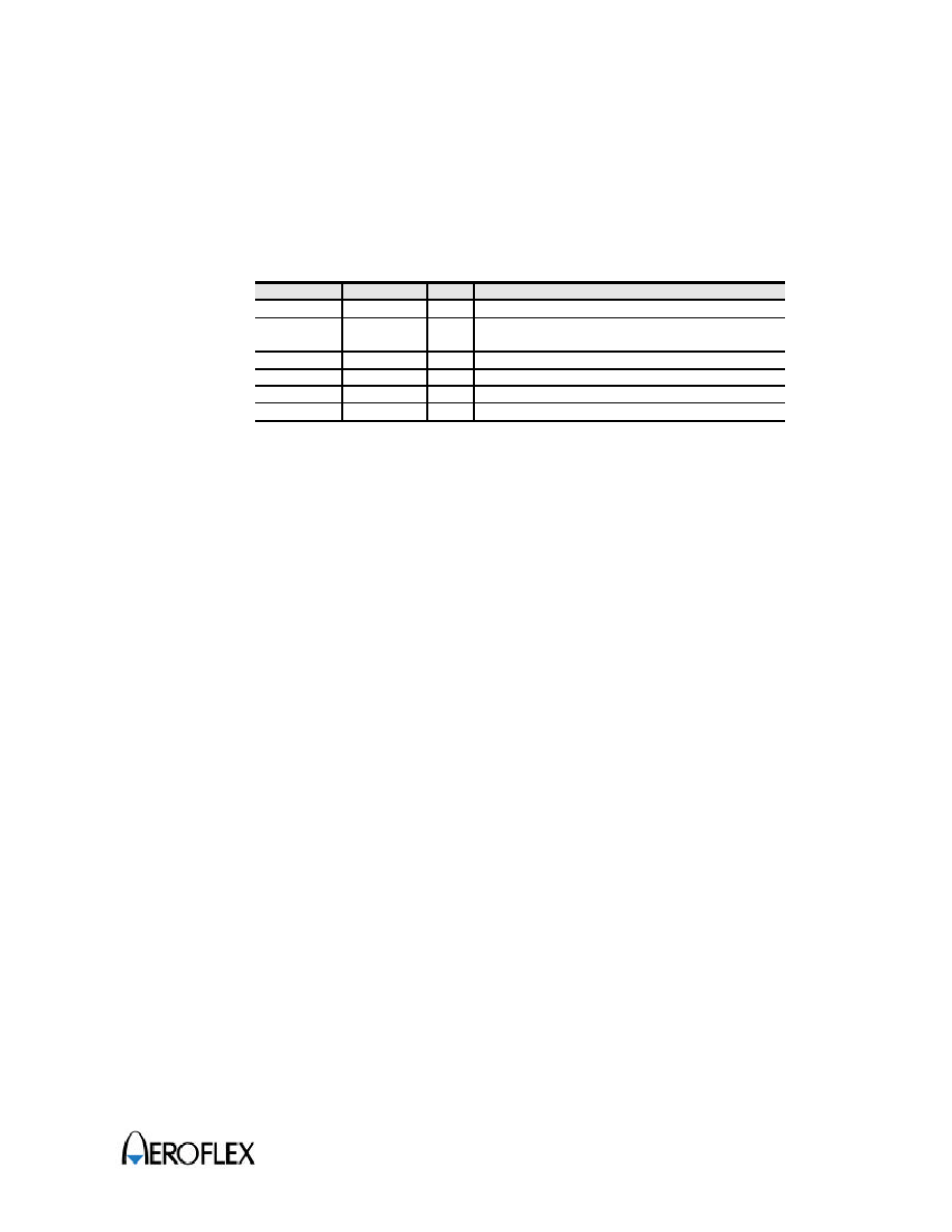
Chapter 5
AX07CF192
76
5.3
Power Management Unit Register Map
The start address of the PMU (Power Management Unit) is 0x0900_1000.
Table 5.1 Register Map of the PMU
Name
I/O Offset
DIR
Description
PMUCR
0x1000
W
PMU operation mode control register.
PMUSR
0x1000
R
PMU status register shows the immediately
prior PMU state.
PCLKCR
0x1008
R/W
Peripheral clock control register.
MEMSR
0x100C
R
Memory remap status register.
MEMCR
0x1010
W
Memory remap control register
RSTCR
0x1030
W
Soft-Reset control register

Chapter 5
AX07CF192
77
5.4
Register Description
The PMU supplies the clock to all of the blocks in the MCU. The start address of the register
is 0x0900_1000.
PMUCR
PMU Control Register (0x0900_1000 Write-Only)
b31 - b8
b7
b6
b5
b4
b3
b2
b1
b0
PMUCR
Reserved
PD
Reset
-
0
0
0
0
0
0
0
0
Initial value : 0x-00
PD
11 : Entering the Power down Mode
00 : Clear PMU Status Register
This register controls the operation mode of the PMU. After a power on reset the register
value is initialized to 00. If PMUCR is written to 11, the device enters the PD (Power Down)
mode. Writing other values does not affect the device. The address of the register is
0x0900_1000.
PMUST
PMU Status Register (0x0900_1000 Read-Only)
b31 - b8
b5
b4
b3
b2
b1
b0
PMUST
Reserved
PMUST
Reserved
PMUST
Reset
-
0
0
-
0
0
Initial value : 0x-00
This register holds the previous status and reset state of PMU. The address of the register
is 0x0900_1000.
PMUST [5:4] (Previous Reset Status bits)
00 � The Power-On reset state (nPOR)
01 � PMU Soft-reset state
10 � WDT Soft-reset state (after MNRESET)
11 � WDT Overflow-reset state (after PORESET)
PMUST [1:0] (PMU Status bits)
00 � Start after Power-On reset
01 � reserved state
10 � reserved state
11 � Start after Power-Down mode

Chapter 5
AX07CF192
78
PCLKCR
Clock Control Register (0x0900_1008 R/W)
b31 - b16
b15
b14
b13 b12 b11 b10
b9
b8
b7
b6
B5
b4
b3
b2
b1
b0
PCLKCR Reserved WU_SEL INTC_CC
WDT_CC
UART_Clk
UART_CC
TIMER_CC
ADC_CC
Reset
-
0
0
0
0
0
0
0
0
0
0
0
0
0
0
0
0
Initial value : 0x00000000
The address of register is 0x0900_1008.
WU_SEL : Wake-up source interrupt select register
0 - MCU wake-up when nFIQ interrupt occurs
1 - MCU wake-up when nIRQ interrupt occurs
INTC_CC : Interrupt controller clock control register
0 - Interrupt controller uses the XIN clock. XIN is not killed in any
mode
1 - Interrupt controller uses the BCLK of the internal Bus clock. The
Bus clock is killed when in Power-down mode
WDT_CC : Clock control register of WDT
000 - BCLK
001 - BCLK/2
010 ~ 111 � Reserved
UART_ Clk : UART0,1 clocks on-off control register.
00 - UART0,1 clocks ON
01 - UART1 clock ON, UART0 clock OFF
10 - UART1 clock OFF, UART0 clock ON
11 � UART0,1 clocks OFF
UART_ CC : Clock Control register of UART.
000 - BCLK
001 - BCLK/2
010 ~ 111 � Reserved
TIMER_ CC : Clock Control register of TIMER.
000 - BCLK
001 - BCLK/2
010 ~ 111 � Reserved
ADC_CC : Clocks Control register of ADC.
Values are the same as WDT_CC

Chapter 5
AX07CF192
79
MEMCR
Memory map Control Register (0x0900_1010 Write-Only)
MEMSR
Memory map Status Register (0x0900_100C Read-Only)
b31 - b3
b2
b1
b0
MEMCR
MEMSR
Reserved
SM
On-Flash
REMAP
Reset
-
0
0
0
Initial value : 0x-0
During write operation, the address of the register is 0x0900_1010 and during read
operation, the address of the register is 0x0900_100C.
SM : External bus controller mapping change.
0 - Each nCS0 ~ nCS7 of address space is 16MB in size
1 - Each nCS0 ~ nCS7 of address space is 1MB in size
On-Flash : Re-mapping of Flash start address to 0x0 in MODES 6
and 7.
0 - Default value.
1 - Re-mapping of Flash start address to 0x0 in the memory map. It
is valid in MODES 6 and 7.
REMAP : Re-map internal SRAM address location.
0 - internal SRAM at 0x0803_0000
1 - Re-mapping of internal SRAM start address to 0x0 in the
memory map. It is used in MODES 2,3,4,5,6 and 7.
RSTCR
Soft-Reset Control Register (0x0900_1030 Write-Only)
b31 - b1
b0
RSTCR
Reserved
RSTCR
Reset
-
-
RSTCR 1 : Software-reset
0 : Normal
This register is used for generating Soft-reset operation. The MCU enters into the reset
state when this register is set high. It is cleared automatically at the end of the Soft-Reset.
The address is 0x0900_1030.

Chapter 5
AX07CF192
80
5.5
Signal Timing Diagram
The PMU signal timing is as shown below.
5.5.1
Power on Reset
Figure 5.3 Power on Reset Timing Diagram
5.5.2
Watch Dog Timer Overflow
Figure 5.4 Watchdog Timer Overflow Timing Diagram
BCLK
PORESET
BnRES
512 clks
CLKIN
XnRES
BnRES
32 clks

Chapter 5
AX07CF192
81
5.5.3
Soft-Reset
There are two Soft-Reset cases. The first Soft-Reset operation is initiated by the
MAN_RST signal from the WDT.
The other is from the PMU reset control register.
Figure 5.5 Soft Reset (from WDT) Timing Diagram
Figure 5.6 Soft Reset (from PMU) Timing Diagram
BCLK
MAN_RST
BnRES
512 clks
BCLK
RSTCR
BnRES
512 clks

Chapter 8
AX07CF192
82
Chapter 6
The Interrupt Controller

Chapter 8
AX07CF192
83
6.1
About the Interrupt controller
The interrupt controller has the following features :
�
Asynchronous interrupt controller
�
8 external interrupt sources
�
13 internal interrupt sources
�
Low interrupt latency
�
Selectable level- or edge-trigger on all interrupt source inputs
�
Each interrupt source and output signal is maskable
�
Selectable output paths (IRQ or FIQ) for each interrupt source
Mask
Control
IRQ source0
IRQ source20
IRQ source1
IRQ source2
IRQ source3
IRQ source4
IRQ source5
IRQ source15
IRQ source16
IRQ source17
IRQ source18
IRQ source19
Edge/
Level
Control
High/
Low,
Rising/
Falling
Control
FIQ
or
IRQ
IRQ
FIQ
IRQ
Mask
FIQ
Mask
nFIQ
nIRQ
Source Mask
Control
Trigger Mode
Control
Polarity
Control
Direction
Control
Status
Control
Request
Control
Clear Control
21
21
21
21
21
21
Figure 6.1 Interrupt Control Flow Diagram

Chapter 8
AX07CF192
84
6.1.1
Interrupt sources
The interrupt controller provides an interface between multiple interrupt sources and the
processor. The interrupt controller supports internal and external interrupt sources.
Internally there are 11 peripheral interrupt sources. Externally there are 8 interrupt sources.
Therefore certain interrupt bits can be defined for the basic functionality required in any
system, while the remaining bits are available for use by other devices in any particular
implementation.
Table 6.1 Interrupt Controller Default Setting Value
Interrupt No.
INTERRUPT SOURCES
INT0
External Interrupt 0
INT1
External Interrupt 1
INT2
External Interrupt 2
INT3
External Interrupt 3
INT4
External Interrupt 4
INT5
External Interrupt 5
INT6
External Interrupt 6
INT7
External Interrupt 7
INT8
reserved
INT9
reserved
INT10
WDT
INT11
UART0
INT12
UART1
INT13
ADC
INT14
Timer 0
INT15
Timer 1
INT16
Timer 2
INT17
Timer 3
INT18
Timer 4
INT19
Timer 5
INT20
Software Interrupt
The user can set the active mode of all interrupt source inputs. The default mode is falling-
edge triggered. Any inversion or latching required to provide edge sensitivity must be
provided at the generating source of the interrupt.
No hardware priority scheme or any form of interrupt vectoring is provided, but the priority
can be determined using the FIQ and IRQ mask registers under software control.
The FIQ and IRQ mask registers may also be used to generate an interrupt under software
control. Typically these registers are used to determine whether either an FIQ or IRQ
interrupt is generated.

Chapter 8
AX07CF192
85
6.1.2
Interrupt Control
The interrupt controller provides the interrupt source status and the interrupt request status.
The interrupt mask registers are used to determine whether an active interrupt source
should generate an interrupt request to the processor or not. A logic-level HIGH in the
interrupt mask register indicates that the interrupt source is masked and will not generate a
request.
The FIQ and IRQ mask registers indicate whether the interrupt source causes a processor
interrupt or not.
The interrupt modes are configurable by the interrupt trigger mode and interrupt trigger
polarity registers. The Interrupt direction register indicates whether each interrupt source
drives IRQ or FIQ.
The FIQ and IRQ status register is used to reflect the status of all channels set to produce
an FIQ interrupt or IRQ interrupt. The status registers are cleared by writing `1' to the ISCR
register in edge trigger mode only.
Bit 20 is used as a software interrupt source. When source mask control register bit 20 is
HIGH, an interrupt request occurs. To disable the software interrupt, Source Mask Control
Register bit 20 should be Low. The Software interrupt source input is fixed active HIGH and
level sensitive.

Chapter 8
AX07CF192
86
6.2
Interrupt Controller Registers
The start address of the interrupt controller is 0x0900_1200. The offset of any particular
register from the start address is fixed. The following registers are provided for both FIQ
and IRQ interrupt controllers:
Table 6.2 Memory Map of the Interrupt Controller
REG.
I/O OFFSET
Dir
Description
GMR
0x1200
R/W
Global Mask Register
TMR
0x1204
R/W
Trigger Mode Register
TPR
0x1208
R/W
Trigger Polarity Register
IDR
0x120C
R/W
Interrupt Direction Register
FSR
0x1210
R
FIQ Status Register
ISR
0x1214
R
IRQ Status Register
FMR
0x1218
R/W
FIQ Mask Register
IMR
0x121C
R/W
IRQ Mask Register
ISCR
0x1220
W
Interrupt Status Clear Register
GMR
Global Mask Register (0x0900_1200 R/W)
b31 - b21
b20b19b18b17b16b15b14b13b12b11 b10 b9 b8 b7 b6 b5 b4 b3 b2 b1 b0
GMR
Reserved
I20 I19 I18 I17 I16 I15 I14 I13 I12 I11 I10 I9 I8 I7 I6 I5 I4 I3 I2 I1 I0
Reset
0000000
1
1
1
1
1
1
1
1
1
1
1
1
1 1
1
1
1
1
1
1
1
Initial value : 0x01FFFFF
Bit field I0-I24
1 : Mask
0 : Unmask
The interrupt mask register is used to mask the interrupt input sources and defines which
active sources will generate an interrupt request to the processor. If certain bits within the
interrupt controller are not implemented, the corresponding bits in the interrupt mask
register must be masked. A bit value of 0 indicates that the interrupt is unmasked and will
allow an interrupt request to reach the processor. A bit value of 1 indicates that the interrupt
is masked. Once a bit is masked, the corresponding bit in the status register is cleared. On
reset, all interrupt input-sources are masked.
TMR
Trigger Mode Register (0x0900_1204 R/W)
b31 - b21
b20b19b18b17b16b15b14b13b12b11 b10 b9 b8 b7 b6 b5 b4 b3 b2 b1 b0
TMR
Reserved
I20 I19 I18 I17 I16 I15 I14 I13 I12 I11 I10 I9 I8 I7 I6 I5 I4 I3 I2 I1 I0
Reset
0000000
0
0
0
0
0
0
0
0
0
0
0
0
0 0
0
0
0
0
0
0
0
Initial value : 0x0100000
Bit field I0-I24
1 : Level Trigger Mode
0 : Edge Trigger Mode
The interrupt trigger mode register is used to configure the interrupts in conjunction with the
interrupt trigger polarity register. Each interrupt can be configured to be level or edge
triggered. A bit value of 0 indicates that the interrupt is configured to be edge triggered and
a bit value of 1 indicates that the interrupt is level triggered. On reset, all interrupt input
sources are configured to be edge triggered.

Chapter 8
AX07CF192
87
TPR
Trigger Polarity Register (0x0900_1208 R/W)
b31 - b21
b20b19b18b17b16b15b14b13b12b11 b10 b9 b8 b7 b6 b5 b4 b3 b2 b1 b0
TPR
Reserved
I20 I19 I18 I17 I16 I15 I14 I13 I12 I11 I10 I9 I8 I7 I6 I5 I4 I3 I2 I1 I0
Reset
0000000
0
0
0
0
0
0
0
0
0
0
0
0
0 0
0
0
0
0
0
0
0
Initial value : 0x01000000
Bit field I0-I24
1 : High/Rising Edge
0 : Low/Falling Edge
The interrupt trigger polarity register is used to configure the interrupts in conjunction with
the interrupt trigger mode register. Each interrupt can be configured to be rising/high or
falling/low active. A bit value of 0 indicates that the interrupt is configured to be falling active
for edge trigger mode and low active for level trigger mode. A bit value of 1 indicates that
the interrupt is configured to be rising active for edge trigger mode and high active for level
trigger mode. On reset, all interrupt input sources are configured to be falling/low active.
Table 6.3 Interrupt Source Trigger Mode
DETECTION MODE
TMR
TPR
Falling-Edge (Default)
0
0
Rising-Edge
0
1
Low-Level
1
0
High-Level
1
1
IDR
Interrupt Direction Register (0x0900_120C R/W)
b31 - b21
b20b19b18b17b16b15b14b13b12b11 b10 b9 b8 b7 b6 b5 b4 b3 b2 b1 b0
IDR
Reserved
I20 I19 I18 I17 I16 I15 I14 I13 I12 I11 I10 I9 I8 I7 I6 I5 I4 I3 I2 I1 I0
Reset
0000000
0
0
0
0
0
0
0
0
0
0
0
0
0 0
0
0
0
0
0
0
0
Initial value : 0x00000000
Bit field I0-I24
1 : Direction to FIQ
0 : Direction to IRQ
The interrupt direction register is used to determine whether each interrupt source drives
IRQ or FIQ. A bit value of 0 indicates that the interrupt is driven to IRQ and a bit value of 1
indicates that the interrupt is driven to FIQ. On reset, all interrupt input sources drive IRQ.

Chapter 8
AX07CF192
88
FSR
FIQ Status Register (0x0900_1210 Read Only)
b31 - b21
b20b19b18b17b16b15b14b13b12b11 b10 b9 b8 b7 b6 b5 b4 b3 b2 b1 b0
FSR
Reserved
I20 I19 I18 I17 I16 I15 I14 I13 I12 I11 I10 I9 I8 I7 I6 I5 I4 I3 I2 I1 I0
Reset
0000000
0
0
0
0
0
0
0
0
0
0
0
0
0 0
0
0
0
0
0
0
0
Initial value : 0x00000000
Bit field I0-I24
1 : FIQ Pending
0 : FIQ Idle
The FIQ status register is used to reflect the status of all channels set to produce an FIQ
interrupt (IDRn = 1). When an interrupt is set for an FIQ to occur, the corresponding bit is
set in the FIQ status register. The interrupt handler will examine this register to determine
the channel(s) that caused the FIQ interrupt. When the status clear register is written to `1',
the corresponding bit is cleared if that channel is configured for edge trigger mode. A HIGH
bit indicates that the interrupt is active and will generate an interrupt to the processor.
ISR
IRQ Status Register (0x0900_1214 Read Only)
b31 - b21
b20b19b18b17b16b15b14b13b12b11 b10 b9 b8 b7 b6 b5 b4 b3 b2 b1 b0
ISR
Reserved
I20 I19 I18 I17 I16 I15 I14 I13 I12 I11 I10 I9 I8 I7 I6 I5 I4 I3 I2 I1 I0
Reset
0000000
0
0
0
0
0
0
0
0
0
0
0
0
0 0
0
0
0
0
0
0
0
Initial value : 0x00000000
Bit field I0-I24
1 : IRQ Pending
0 : IRQ Idle
The IRQ status register is used to reflect the status of all channels set to produce an IRQ
interrupt (IDR(i) = 0). When an interrupt is set for an IRQ to occur, the corresponding bit is
set in the IRQ status register. The interrupt handler will examine this register to determine
the channel(s) that caused the IRQ interrupt. When the status clear register is written to `1',
the corresponding bit is cleared if that channel is configured for edge trigger mode. A HIGH
bit indicates that the interrupt is active and will generate an interrupt to the processor.
FMR
FIQ Mask Register (0x0900_1218 R/W)
b31 - b21
b20b19b18b17b16b15b14b13b12b11 b10 b9 b8 b7 b6 b5 b4 b3 b2 b1 b0
FMR
Reserved
I20 I19 I18 I17 I16 I15 I14 I13 I12 I11 I10 I9 I8 I7 I6 I5 I4 I3 I2 I1 I0
Reset
0000000
0
0
0
0
0
0
0
0
0
0
0
0
0 0
0
0
0
0
0
0
0
Initial value : 0x00000000
Bit field I0-I24
1 : Disable FIQ
0 : Enable FIQ
The FIQ request mask register is used to mask the request to generate an interrupt to the
processor. If certain bits within the interrupt controller are not implemented, the
corresponding bits in the FIQ request mask register must be masked. A bit value of 0
indicates that the interrupt is unmasked and will allow an interrupt request to reach the
processor. A bit value of 1 indicates that the interrupt is masked. On reset, all FIQ requests
are unmasked.

Chapter 8
AX07CF192
89
IMR
IRQ Mask Register (0x0900_121C R/W)
b31 - b21
b20b19b18b17b16b15b14b13b12b11 b10 b9 b8 b7 b6 b5 b4 b3 b2 b1 b0
IMR
Reserved
I20 I19 I18 I17 I16 I15 I14 I13 I12 I11 I10 I9 I8 I7 I6 I5 I4 I3 I2 I1 I0
Reset
0000000
0
0
0
0
0
0
0
0
0
0
0
0
0 0
0
0
0
0
0
0
0
Initial value : 0x00000000
Bit field I0-I24
1 : Disable IRQ
0 : Enable IRQ
The IRQ request mask register is used to mask the request to generate an interrupt to the
processor. If certain bits within the interrupt controller are not implemented, the
corresponding bits in the IRQ request mask register must be masked. A bit value of 0
indicates that the interrupt is unmasked and will allow an interrupt request to reach the
processor. A bit value of 1 indicates that the interrupt is masked. On reset, all IRQ requests
are unmasked.
ISCR
Interrupt Status Clear Register (0x0900_1220 Write Only)
b31 - b21
b20b19b18b17b16b15b14b13b12b11 b10 B9 b8 b7 b6 b5 B4 b3 b2 b1 b0
ISCR
Reserved
I20 I19 I18 I17 I16 I15 I14 I13 I12 I11 I10 I9 I8 I7 I6 I5 I4 I3 I2 I1 I0
Reset
0000000
0
0
0
0
0
0
0
0
0
0
0
0
0 0
0
0
0
0
0
0
0
Initial value : 0x00000000
Bit field I0-I24
1 : Clear Interrupt Status
0 : No action
The status clear register is used to clear bits in the status register configured for edge
trigger mode. If the channels are configured for level trigger mode, the corresponding bits in
the FIQ status register and the IRQ status register have no effect. This register is cleared
when written to `1'. When writing to this register, each data bit that is HIGH causes the
corresponding bit in the status register to be cleared. Data bits that are LOW have no effect
on the corresponding bit in the status register. Note that the status clear register has an
effect on the status register in the edge trigger mode.

Chapter 8
AX07CF192
90
Chapter 7
Watchdog Timer

Chapter 8
AX07CF192
91
7.1
General Description
�
Watchdog timer mode and Interval timer mode
�
Generates interrupt signal (INT_WDT) to the interrupt controller in either mode
�
Outputs signals PORESET and MNRESET to the PMU (Power Management Unit)
�
Eight counter clock sources
�
Selection whether to reset the chip internally or not
�
Two types of reset signal : power-on reset and manual reset
Figure 7.1 Watchdog Timer Module Block Diagram
TCNT : Timer Counter (8-bit)
TRCR : Timer/Reset Control Register (8-bit)
RSTSR : Reset Status Register (2-bit)
System Clock
Module data bus
RSTSR
Clock
Generation
Clock
Selection
Internal
Signals
TCNT
Overflow
Reset
Control
Interrupt
Control
Control Logic
Clock
INT_WDT
PORST
MNRST
Bus
Interface
TRCR

Chapter 8
AX07CF192
92
7.2
Watchdog Timer Introduction
The AX07CF192 has a one-channel watchdog timer (WDT) for monitoring system
operations. If the system locks up and the timer counter overflows without being rewritten
correctly by the CPU, a reset signal is output to PMU.
When this watchdog function is not needed, the WDT can be used as an interval timer. In
the interval timer mode, an interval timer interrupt is generated at each counter overflow.
The WDT has a clock generator that produces eight counter clock sources. The clock
signals are obtained by dividing down the frequency of the system clock. Users can select
one of eight internal clock sources for input to the WTCNT by means of CKS2 - CKS0 in the
WTCR.

Chapter 8
AX07CF192
93
7.3
Watchdog Timer Operation
The Watchdog Timer Mode
To use the WDT as a watchdog timer, set the WT/nIT and TMEN bits of the WTCR to a logic
1. Software must prevent WTCNT overflow by rewriting the TCNT value (normally by writing
0x00) before overflow occurs. If the WTCNT fails to be rewritten and overflows due to a
system crash or the like, the INT_WDT and PORESET /MNRESET signals are output. The
INT_WDT signal is not output if INTEN is disabled (INTEN = 0).
WTCNT
value
Time
0x00
0xFF
0x00 written in
WTCNT
WTOVF = 1
FAULT and internal reset generated
TMEN = 1
WT/nIT = 1
Figure 7.2 Operation in the Watchdog Timer Mode
If the RSTEN bit in the WTCR is set to 1, a signal to reset the chip will be generated
internally when TCNT overflows. Either a power-on reset or a manual reset can be selected
by the RSTSEL bit.

Chapter 8
AX07CF192
94
The Interval Timer Mode
To use the WDT as an interval timer, clear WT/nIT to 0 and set TMEN to 1. A watchdog
timer interrupt (INT_WDT) is generated each time the timer counter overflows. This function
can be used to generate interval timer interrupts at regular intervals.
WTCNT
value
Time
0x00
0xFF
ITOVF = 1
WDTINT generated
TMEN = 1
WT/nIT = 0
Figure 7.3 Operation in the Interval Timer Mode
7.3.1
Timing of Setting and Clearing the Overflow Flag
Timing of setting the overflow flag
In the interval timer mode when the WTCNT overflows, the ITOVF flag is set to 1 and
watchdog timer interrupt (INT_WDT) is requested.
In the watchdog timer mode when the WTCNT overflows, the WTOVF bit of the SR is set to
1 and a WDTOUT signal is output. When the RSTEN bit is set to 1, a WTCNT overflow
causes an internal reset signal to be generated for the entire chip.
Timing of clearing the overflow flag
When the Reset Status Register (WRSR) is read, the overflow flag is cleared.

Chapter 8
AX07CF192
95
7.4
Watchdog Timer Memory Map
The WDT has five registers. They are used to select the internal clock source, switch to the
WDT mode, control the reset signal, and test it. The start address of the watchdog timer is
fixed to 0x0900_1100 and the offset of any particular register from the base address is
fixed.
Table 7.1 Memory Map of the Watchdog Timer APB Peripheral
Name
I/O Offset
DIR
Description
WTCR
0x1100
R/W
WDT control. (8-bit)
WRSR
0x1104
R
WDT Reset status reg. (2-bit)
WTCNT
0x1108
R/W
WDT Timer counter. (8-bit)

Chapter 8
AX07CF192
96
7.5
Watchdog Timer Register Descriptions
The following registers are provided for the watchdog timer:
WTCR
Watchdog Timer Control Register ( 0x0900_1100 R/W )
b31 - b8
b7
b6
b5
b4
B3
b2
b1
b0
WTCR
Reserved
INTEN
WT/nIT
TMEN
RSTEN
RSTSEL
CKSEL
Reset
-
0
0
0
0
0
0
0
0
Initial value : 0x-00
CKSEL : Clock select. Select one of eight internal clock
sources for input to the WTCNT.
000 � BCLK / 2
001 � BCLK / 8
010 � BCLK / 32
011 � BCLK / 64
100 � BCLK / 256
101 � BCLK / 512
110 � BCLK / 2048
111 � BCLK / 8192
RSTSEL : Reset select register. Select the type of internal
reset generated if WTCNT overflows in the watchdog timer
mode.
0 - Power-on reset
1- Manual reset
RSTEN : Reset enable register. Select whether to reset
the chip internally or not if WTCNT overflows in the
watchdog timer mode.
0 - Disable
1- Enable
TMEN : Timer enable register. Enable or disable the timer.
0 - Disable
1- Enable.
WT/nIT : Timer mode select register. Select whether to use
the WDT as a watchdog timer or interval timer.
0 - Interval timer mode
1- Watchdog timer mode
INTEN : Interrupt enable register. Enable or disable the
interrupt request, INT_WDT.
0 - Disable
1- Enable

Chapter 8
AX07CF192
97
8-bit read / write register. The start address of register is 0x0900_1100.
The following functions are provided :
�
Select the timer mode
�
Select the internal clock source
�
Select the reset mode
�
Set the timer enable bit
�
Enable interrupt request
�
Enable reset signal occurrence
The clock signals are obtained by dividing down the system clock.
Table 7.2 Internal Counter Clock Sources (SYSCLK = 40 MHz)
CKSEL
CLOCK SOURCE
OVERFLOW INTERVAL
000
SYSCLK / 2
12.8 us
001
SYSCLK / 8
51.2 us
010
SYSCLK / 32
204.8 us
011
SYSCLK / 64
409.6 us
100
SYSCLK / 256
1.64 ms
101
SYSCLK / 512
3.28 ms
110
SYSCLK / 2048
13.11 ms
111
SYSCLK / 8192
52.43 ms
WRSR
Reset Status Register ( 0x0900_1104 Read-Only )
b31 - b2
b1
b0
WRSR
Reserved
ITOVF
WTOVF
Reset
-
0
0
Initial value : 0x-0
1 : Overflowed
0 : Normal
WTOVF : Watchdog timer overflow flag. Indicates that the
WTCNT has overflowed in the watchdog timer mode.
ITOVF : Interval timer overflow flag. Indicates that the
WTCNT has overflowed in the watchdog timer mode.
Two-bit read only register. The WRSR indicates whether WTCNT has overflowed or not.
The WRSR is initialized to 0x0 by the reset signal, BnRES.
Bit 0 (WTOVF) indicates that the WTCNT has overflowed in the watchdog timer mode. Bit 1
(ITOVF) indicates that the WTCNT has overflowed in the interval timer mode.
WTCNT
Watchdog Timer Counter ( 0x0900_1108 R/W )
b31 - b8
b7
b6
b5
b4
b3
b2
b1
b0
WTCNT
Reserved
I7
I6
I5
I4
I3
I2
I1
I0
Reset
-
0
0
0
0
0
0
0
0
Initial value : 0x-00
Bit field I0-I7
8-bit read / write upcounter. When the timer is enabled, the timer counter starts counting
pulses from the selected clock source. When the value of the WTCNT changes from 0xFF-
0x00(overflows), a watchdog timer overflow signal is generated in both timer modes. The
WTCNT is initialized to 0x00 by a power-reset (nB_RES).

Chapter 8
AX07CF192
98
7.6
Examples of Register Setting
7.6.1
Interval Timer Mode
WTCNT = 0x00
WTCR = 0xA0
WTCR
WDTINT
WRSR
PORESET
MNRESET
OVERFLOW
WTCNT
SCLK
MAIN-CLK
FE
FF
00
01
10
11
12
13
14
`0
`0'
0xA0
0xA0
2'b00
2'b10
2'b00
Read RSTSR
Figure 7.4 Interrupt Clear in the Interval Timer Mode

Chapter 8
AX07CF192
99
7.6.2
Watchdog Timer Mode with Internal Reset Disable
WTCNT = 0x00 (normally)
WTCR = 0xE0
Figure 7.5 Interrupt Clear in the Watchdog Timer Mode with Reset Disable
WDCR
WDTINT
WDSR
PORESET
MNRESET
OVERFLOW
WTCNT
XIN
MAIN-CLK
FE
FF
00
01
10
11
12
13
14
2'b00
2'b01
2'00
`0
`0'
0xE0
0xE0
Read RSTSR Register

Chapter 8
AX07CF192
100
7.6.3
Watchdog Timer Mode with Power-on Reset
WTCNT = 0x00
WTCR = 0xF0
Figure 7.6 Interrupt Clear in the Watchdog Timer Mode with Power-on Reset
WDCR
WDTINT
WDSR
PORESET
MNRESET
OVERFLOW
WTCNT
XIN
MAIN-CLK
FE
FF
00
01
10
11
12
00
2'b00
2'b01
2'b00
`0
0xF0
0xF0
`0
Reset

Chapter 8
AX07CF192
101
7.6.4
Watchdog Timer Mode with Manual Reset
WTCNT = 0x00
WTCR = 0xF8
Figure 7.7 Interrupt Clear in the Watchdog Timer Mode with Manual Reset
WDCR
WDTINT
WDSR
PORESET
MNRESET
OVERFLOW
WTCNT
XIN
MAIN-CLK
FE
FF
00
01
10
11
12
13
14
2'b00
2'b01
2'00
`0
`0'
0xF8
0xF8

Chapter 8
AX07CF192
102
Chapter 8
The General Purpose Timer

Chapter 8
AX07CF192
103
8.1
About the General Purpose Timer Unit
The general-purpose timer unit has:
�
Six channels with 16-bit counters
�
12 different pulse outputs and 12 different pulse inputs
�
Independent functionality with 12 general registers
�
Compare match waveform output function
�
Input capture function
�
Counter-clearing function at compare match or input capture mode
�
Synchronizing mode
�
PWM mode
�
18 interrupt sources
�
Selectable 4 internal clock sources and 4 external clock sources
Internal
data bus
Clock
Generation
Clock
Selection
Control
PCLK
16
-
bit timer channel1
16
-
bit timer channel0
16
-
bit timer channel2
16
-
bit timer channel3
Module data bus
16
-
bit timer channel4
TINT0
-
TINT5
TIOCA0 � TIOCA5
TIOCB0 � TIOCB5
16
-
bit timer channel5
Bus Interface
TSTARTR
TSYNR
TPWMR
TCLKA - TCLKD
Figure 8.1 General-purpose Timer Unit Module Block Diagram

Chapter 8
AX07CF192
104
8.1.1
General Purpose Timer Unit Introduction
The AX07CF192 has a general-purpose timer unit (GPTU) with six channels of 16-bit
timers. There are two counter operation modes: a free-running mode and a periodic mode.
Each channel has independent operating modes. There are common functions for each
channel: counter operation, input capture, compare match, PWM, and synchronized clear
and write.
It is possible to select one of eight counter clock sources for all channels.
�
Internal clock : counting at falling edge
BCLK / 2
BCLK / 4
BCLK / 16
BCLK / 64
�
External clock: counting at falling edge.
There are five operating modes which can be configured individually. The operating modes
are.
�
Free Running Mode
�
Compare Match Mode
�
Input Capture Mode
�
Synchronized Clear and Write Mode
�
PWM(Pulse-Width-Modulation) Mode
There are four kinds of counter clear sources which are user selectable.
�
None : never clear until overflow for free running mode
�
GRA match or TPA input capture
�
GRB match or TPB input capture
�
Synchronous clear

Chapter 8
AX07CF192
105
8.2
General Purpose Timer Unit Memory Map
8.2.1
Register Assignment
The base address of the general-purpose timer unit is 0x0900_1300 and the offset of any
particular register from the base address is fixed.
Table 8.1 Timer Global Control Register Map
REG.
I/O
OFFSET
DIR.
DESCRIPTION
TSTARTR
0x1300
R/W
Timer Start Register
TSYNCR
0x1304
R/W
Timer Sync. Register
TPWMR
0x1308
R/W
Timer PWM Mode Register
-
0x130C
W
(test only)
-
0x1310
R
(test only)
-
0x1314
W
(test only)
-
0x1318
R
(test only)
Table 8.2 Timer Channel Control Register Map
REG.
I/O
OFFSET
DIR.
DESCRIPTION
TCR0
0x1320
R/W
Timer 0 Control Register
TIOCR0
0x1324
R/W
Timer 0 I/O Control Register
TIER0
0x1328
R/W
Timer 0 Interrupt Enable Register
TSR0
0x132C
R
Timer 0 Interrupt Status Register
TCNT0
0x1330
R/W
Timer 0 Counter Register
GRA0
0x1334
R/W
Timer 0 General Register A
GRB0
0x1338
R/W
Timer 0 General Register B
GP Timer Unit has consists of six unit timer channels and each address starts as follows:
Table 8.3 Timer Channel Starting Address
Timer No.
Starting Offsets
Timer 0
0x1320
Timer 1
0x1340
Timer 2
0x1360
Timer 3
0x1380
Timer 4
0x13A0
Timer 5
0x13D0

Chapter 8
AX07CF192
106
8.2.2
General Purpose Timer Unit Register Descriptions
The base address of the general-purpose timer unit is 0x0900_1300. The following registers
are provided for the general purpose timer unit :
8.2.2.1
Timer Global Control Registers
TSTARTR
Timer Start Register (0x0900_1300 R/W)
b31 b8
b7
b6
b5
b4
b3
b2
b1
b0
TSTARTR
Reserved
res
res
STR5
STR4
STR3
STR2
STR1
STR0
Reset
-
1
1
0
0
0
0
0
0
Initial value : 0xXXXXXXC0
STRn
1 : Start Timer Channel n
0 : Stop Timer Channel n
8-bit read / write register that starts and stops the counter of each channel.
TSYNCR
Timer Sync. Register (0x0900_1304 R/W)
b31 b8
b7
b6
b5
b4
b3
b2
b1
b0
TSYNCR
Reserved
res
res
SYNC5
SYNC4
SYNC3
SYNC2
SYNC1
SYNC0
Reset
-
1
1
0
0
0
0
0
0
Initial value : 0xXXXXXXC0
SYNCn 1 : Operates Synchronously with the other sync.
channel
0 : Independent Counting
8-bit read / write register that selects the timer synchronizing mode for each channel.
TPWMR
Timer PWM Mode Register (0x0900_1308 R/W)
b31 b8
b7
b6
b5
b4
b3
b2
b1
b0
TPWMR
Reserved
res
res
PWM5
PWM4
PWM3
PWM2
PWM1
PWM0
Reset
-
1
1
0
0
0
0
0
0
Initial value : 0xXXXXXXC0
PWMn
1 : PWM Mode
0 : Counter Mode
8-bit read / write register that selects the PWM mode for each channel.

Chapter 8
AX07CF192
107
8.2.2.2
Timer Channel Control Registers
TCR0
Timer 0 Control Register (0x0900_1320 R/W)
0x1340 for Timer 1,0x1360 for Timer 2, 0x1380 for Timer 3, 0x13A0 for Timer 4, 0x13D0 for Timer 5
b31 b8
b7
b6
b5
b4
b3
b2
b1
b0
TCR0
Reserved
res
CCLR
res
res
TPSC
Reset
-
1
00
1
1
000
Initial value : 0xXXXXXX98
CCLR
Select the Counter clear condition
00 : not cleared (free-running mode)
01 : cleared by GRA compare match
or input capture (periodic mode)
10 : cleared by GRB compare match
or input capture (periodic mode)
11 : cleared in synchronization with the
other sync. timer
TPSC
Select the Count clock Source
000 : BCLK/2
001 : BCLK/4
010 : BCLK/16
011 : BCLK/64
100 : Ext CLKA
101 : Ext CLKB
110 : Ext CLKC
111 : Ext CLKD
8-bit readable and writable register for each channel that selects the timer counter clock
source and the counter clear source.

Chapter 8
AX07CF192
108
TIOCR0
Timer 0 I/O Control Register (0x0900_1324 R/W)
0x1344 for Timer 1,0x1364 for Timer 2, 0x1384 for Ti mer 3, 0x13A4 for Timer 4, 0x13D4 for Timer 5
b31 b8
b7
b6
b5
b4
b3
b2
b1
b0
TIOCR0
Reserved
res
IOB
res
IOA
Reset
-
1
00
1
1
000
Initial value : 0xXXXXXX88
IOB
Select GRB Function
000 : compare match with pin output disable
001 : 0 output at GRB compare match
010 : 1 output at GRB compare match
011 : toggle output at GRB compare match
100 : GRB captures the rising edge of input
101 : GRB captures the falling edge of input
110 : GRB captures both edge of input
111 : Don't care
IOA
Select GRA Function
000 : compare match with pin output disable
001 : 0 output at GRA compare match
010 : 1 output at GRA compare match
011 : toggle output at GRA compare match
100 : GRA captures the rising edge of input
101 : GRA captures the falling edge of input
110 : GRA captures both edge of input
111 : Don't care
8-bit read / write register that selects the output compare or input capture function for GRA
and GRB, and selects the function of the TIOCAn and TIOCBn pins. TIOCRn controls the
GRA and GRB.

Chapter 8
AX07CF192
109
TIER0
Timer 0 Interrupt Enable Register (0x0900_1328 R/W)
0x1348 for Timer 1,0x1368 for Timer 2, 0x1388 for Timer 3, 0x13A8 for Timer 4, 0x13D8 for Timer 5
b31 b8
b7
b6
b5
b4
b3
b2
b1
b0
TIER0
Reserved
Res
res
res
res
res
OVFIE
MCIBE
MCIAE
Reset
-
1
1
1
1
1
0
0
0
Initial value : 0xXXXXXXF8
OVFIE 0 : Disable Overflow Interrupt
1 : Enable Overflow Interrupt
MCIBE 0 : Disable GRB Match or
GRB capture Interrupt
1 : Enable GRB Match or
GRB capture Interrupt
MCIAE 0 : Disable GRA Match or
GRA capture Interrupt
1 : Enable GRA Match or
GRA capture Interrupt
8-bit read / write register that controls the enabling/disabling of an overflow interrupt request
and the general register compare match/input capture interrupt requests. TIERn controls the
interrupt enable/disable.
TSR0
Timer 0 Status Register (0x0900_132C Read Only)
0x134C for Timer 1,0x136C for Timer 2, 0x138C for Timer 3, 0x13AC for Timer 4, 0x13DC for Timer 5
b31 b8
b7
b6
b5
b4
b3
b2
b1
b0
TSR0
Reserved
res
res
res
res
res
OVFI
MCIB
MCIA
Reset
-
1
1
1
1
1
0
0
0
Initial value : 0xXXXXXXF8
OVFI
0 : no overflow occurs
1 : Overflow occurs
MCIB
0 : no GRB Match or Capture occurs
1 : GRB Match or Capture occurs
MCIA
0 : no GRA Match or Capture occurs
1 : GRA Match or Capture occurs
8-bit read only register containing the flags that indicate TCNT overflow and GRA/GRB
compare match or input capture. These flags are interrupt sources. Reading this register will
clear all the interrupt flags.

Chapter 8
AX07CF192
110
TCNT0
Timer 0 Counter (0x0900_1330 R/W)
0x1350 for Timer 1,0x1370 for Timer 2, 0x1390 for Timer 3, 0x13B0 for Timer 4, 0x13E0 for Timer 5
b31 b16
B15 b14 b13 b12 b11 b10 b9
b8 B7
b6
b5 b4
b3
b2
b1
b0
TCNT0
Reserved
TCNT
Reset
-
0
0
0
0
0
0
0
0
0
0
0
0
0
0
0
0
Initial value : 0xXXXX0000
TCNT
16bit Counter Value
16-bit read / writle counter. The clock source is selected by the TCR for each channel.
TCNT is cleared to 0x0000 by compare match with the corresponding GRA or GRB, or by
input capture to GRA or GRB. When TCNT is overflow, OVFI in the TSR is set to `1'.
General Register A,B
16-bit read / write register. There are 2 general registers for each channel (total 12). Each
general register can function as either an output compare register or an input capture
register by the setting in the TIOCR.
GRA0
General Register A (0x0900_1334 R/W)
0x1354 for Timer 1,0x1374 for Timer 2, 0x1394 for Timer 3, 0x13B4 for Timer 4, 0x13E4 for Timer 5
b31 b16
b15 b14 b13 b12 b11 b10 b9
b8
b7
b6
b5 b4
b3
b2
b1
b0
GRA0
Reserved
GRA
Reset
-
0
0
0
0
0
0
0
0
0
0
0
0
0
0
0
0
Initial value : 0xXXXX0000
GRA
16bit Compare Match A Value
GRB0
General Register B (0x0900_1338 R/W)
0x1358 for Timer 1,0x1378 for Timer 2, 0x1398 for Timer 3, 0x13B8 for Timer 4, 0x13E8 for Timer 5
b31 b16
b15 b14 b13 b12 b11 b10 b9
b8
b7
b6
b5 b4
b3
b2
b1
b0
GRB0
Reserved
GRB
Reset
-
0
0
0
0
0
0
0
0
0
0
0
0
0
0
0
0
Initial value : 0xXXXX0000
GRB
16bit Compare Match B Value

Chapter 8
AX07CF192
111
8.3
General Purpose Timer Unit Operation
There are five operating modes described below.
�
Free Running Mode
�
Compare Match Mode
�
Input Capture Mode
�
Synchronized Clear and Write Mode
�
PWM(Pulse-Width-Modulation) Mode

Chapter 8
AX07CF192
112
8.3.1
Free Running Mode
A reset of the counters for channels 0 - 5 leaves them all in the free-running mode. When a
corresponding bit in the TSR is set to 1, the corresponding timer counter operates as a free-
running counter and begins to increment. When the count wraps round from 0xFFFF to
0x0000, the overflow flag (OVFI) in the timer status register (TSR) is set to 1. If the OVFIE
bit in the timer's corresponding interrupt enable register (TIER) is set to 1, the CPU will be
asked for an interrupt. After the TCNT overflows, counting continues from 0x0000. Figure
8.2 shows an example of free-running counting.
Periodic counter operation is obtained for a given channel's TCNT by selecting compare
match as a TCNT clear source. (Set the GRA or GRB for period setting to output compare
register and select counter clear upon compare match using the CCLR1 and CCLR0 bits of
the timer control register (TCR). After setting, the TCNT begins incrementing as a periodic
counter when the corresponding bit of TSTARTR is set to 1. When the count matches GRA
or GRB, the MCIA/MCIB bit in the TSR is set to 1 and the counter is automatically cleared
to 0x0000. If the MCIAE/MCIBE bit of the corresponding TIER is set to 1 at this point, the
CPU will be asked for an interrupt. After the compare match, TCNT continues counting from
0x0000. Figure 8.3 shows an example of periodic counting.
Figure 8.2 Free-Running Counter Operation
Time
TCNT value
0xFFFF
STR0-STR4
OVF
0x0000

Chapter 8
AX07CF192
113
Figure 8.3 Periodic Counter Operation
Time
TCNT value
GR
STR0-STR4
OVF
0x0000
Counter cleared by
GR compare match

Chapter 8
AX07CF192
114
8.3.2
Compare Match Mode
Each channel has 2 user settable general registers When the counter reaches the user
programmed value, the channel generates a user-defined interrupt and an external output.
The output value can be '1', '0', or toggle value. The counter can be cleared (user setting)
when a match with the general register is detected.
Figure 8.4 Example of 0 Output/1 Output
Time
TCNT value
0xFFFF
GRB
GRA
Does not change
TIOCB
TIOCA
0 output
1 output
Does not change
Does not change
Does not change

Chapter 8
AX07CF192
115
Figure 8.5 Example of Toggle Output
Figure 8.6 Compare Match Signal Output Timing
Counter cleared at
GRB compare match
TCNT value
GRB
GRA
TIOCB
TIOCA
Toggle
output
Toggle
output
Time
CK
TCNT input
clock
TCNT
GR
Compare
match signal
TIOCA
TIOCB
N
N + 1
N

Chapter 8
AX07CF192
116
8.3.3
Input Capture Mode
When set to input capture mode, at the rising/falling edge of either capture input, TIOCA or
TIOCB, the counter value is transferred to GRA or GRB respectively. Also setting the
MCIAE or MCIBE in TIER the interrupt can be generated by an external capture event. The
capture data and interrupt are generated after 2 timer clocks. If the CCR field in TCR is
appropriately set, the counter will be cleared when the edge of TIOCA or TIOCB is detected.
Figure 8.7 Input Capture Operation
Time
TCNT value
0x0180
TIOCB
TIOCA
0x0160
0x0005
0x0000
GRA
GRB
0x0005
0x0160
0x0180
Counter cleared
by TIOCB input
(falling edge)

Chapter 8
AX07CF192
117
8.3.4
Synchronized Clear and Write Mode
If several channels are set to synchronization mode, and one of them is cleared by a
compare match or input capture, the other channels can also be cleared simultaneously. If
several channels are set to synchronization mode and the user writes to any one of them,
the other channels can also be written with the same value simultaneously.
Figure 8.8 Synchronized Operation Example
Synchronized clear on GRB0 compare match
TCNT0-TCNT2 value
GRB0
GRB1
TIOCA0
TIOCA1
Time
TIOCA2
GRA0
GRB2
GRA1
GRA2
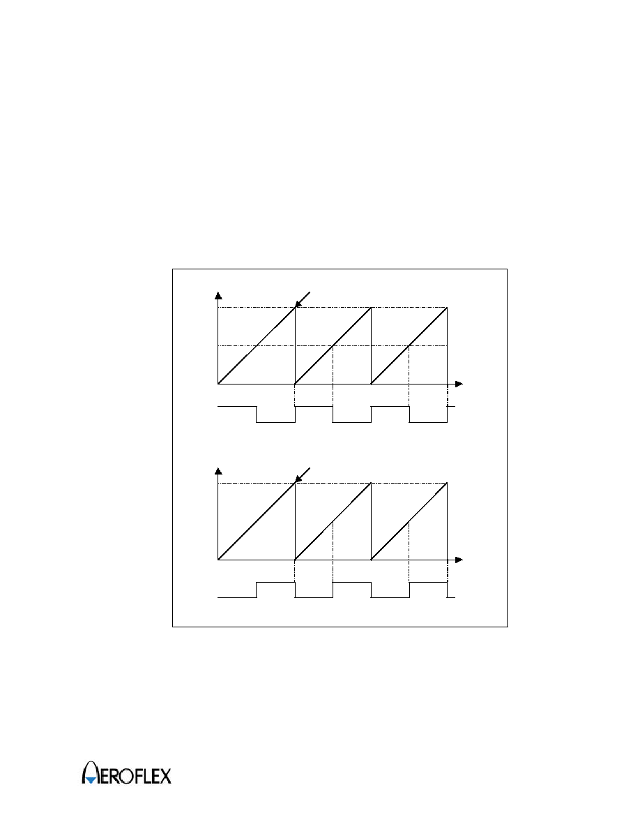
Chapter 8
AX07CF192
118
8.3.5
PWM Mode
The PWM mode is controlled using both the GRA and GRB in pairs. The PWM waveform is
output from the TIOCA output pin. The PWM waveform's 1 output timing is set in GRA and
the 0 output timing is set in GRB. A PWM waveform with duty cycle between 0% and 100%
can be output from the TIOCA pin by having either compare match GRA or GRB be the
counter clear source for the timer counter. All five channels can be set to PWM mode.
8.3.5.1
PWM Mode Operation
Figure 8.9 illustrates PWM mode operations. When the PWM mode is set, the TIOCA pin
becomes the output pin. Output is 1 when the TCNT matches the GRA, and 0 when TCNT
matches the GRB. The TCNT can be cleared by compare match with either GRA or GRB.
This can be used in both free-running and synchronized operation.
Figure 8.9 PWM Mode Operation Example 1
Counter cleared at GRA compare match
TCNT value
GRA
GRB
TIOCA
Time
a. Counter cleared by GRA
Counter cleared at GRB compare match
TCNT value
GRB
GRA
TIOCA
Time
b. Counter cleared by GRB

Chapter 8
AX07CF192
119
Figure 8.10 shows examples of PWM waveforms output with 0% and 100% duty cycles. A
0% duty cycle waveform can be obtained by setting the counter clear source to GRB and
then setting GRA to a larger value than GRB. A 100% duty waveform can be obtained by
setting the counter clear source to GRA and then setting GRB to a larger value than GRA
Figure 8.10 PWM Mode Operation Example 2
Counter cleared on compare match B
TCNT value
GRB
GRA
TIOCA
Time
a. 0% duty
Counter cleared on compare match A
TCNT value
GRB
GRA
Time
0x0000
GRA write
GRA write
TIOCA
b. 100% duty
GRB write
GRB write
0x0000

Chapter 8
AX07CF192
120
Figure 8.11 Reset-Synchronized PWM Mode Operation Example
Reset-Synchronized PWM Mode Operation:
Figure 8.11 shows an example of operation in the reset-synchronized PWM mode. TCNT1
operates as an upcounter that is cleared to 0x0000 at compare match with GRA1. TCNT2
runs independently and is isolated from GRA2 and GRB2. The PWM waveform outputs
toggle at each compare match (GRB1, GRB2, and GRB3 with TCNT1) and when the
counter cleared.
Synchronized clear on GRA1 compare match
TCNT0 value
GRA1,2,3
GRB1
TIOCA1
Time
GRB2
GRB3
TIOCA2
TIOCA3

Chapter 8
AX07CF192
121
Chapter 9
UART (Universal Asynchronous
Receiver/Transmitter)

Chapter 9
AX07CF192
122
9.1
General Description
This module is a Universal Asynchronous Receiver/Transmitter (UART) with FIFOs, and is
functionally identical to the 16550. The UART can be put into an alternate mode (FIFO
mode) to relieve the CPU of excessive software overhead.
In this mode internal FIFOs are activated allowing 16 bytes plus 3 bits of error data per byte
in the RCVR FIFO, to be stored in both receive and transmit modes. All the logic is on the
chip to minimize the system overhead and maximize system efficiency.
The UART performs serial-to-parallel conversion on data characters received from a
peripheral device and parallel-to-serial conversion on data characters received from the
CPU. The CPU can read the complete status of the UART at any time during operation.
Status information includes the type and condition of the transfer operations performed by
the UART, as well as any error conditions (parity, overrun, framing, or break interrupt).
The UART includes a programmable baud rate generator that is capable of dividing the
timing reference clock input by divisors of 1 to 65535 and producing a 16x clock for driving
the internal transmitter logic. Provisions are also included to use this 16x clock to drive the
receiver logic. In addition to baud rate generation, the UART also includes a clock divider
which divides the input system clock by setting an 8-bit divider register.
The UART has a processor interrupt system. Interrupts can be programmed to the user's
requirements, minimizing the computing required to handle the communications link. The
standard 16450/16550 UART features modem control signals which are duplicated
internally, but are concealed from the outside.
Figure 9.1 TOP BLOCK Diagram
P r e s c a l e r
C l o c k
G e n e r a t i o n
U A R T _ C L K
Internal
b u s
U A R T 0
U A R T 1
INT_U A R T [ 1 : 0 ]
UCLK0
Bus Interface
C o n t r o l
E N U C L K 0
E N U C L K 1
UCLK1

Chapter 9
AX07CF192
123
9.2
Features
�
Capable of running all existing 16550 software.
�
After reset, all registers are identical to the 16450 register set.
�
The FIFO mode transmitter and receiver are each buffered with 16-byte FIFO's to reduce
the number of interrupts presented to the CPU.
�
Adds or deletes standard asynchronous communication bits (start, stop, and parity) to or
from the serial data.
�
Hold and shift registers in the 16450 mode eliminate the need for precise synchronization
between the CPU and serial data.
�
Independently controlled transmit, receive, line status and data set interrupts.
�
Programmable baud generator divides any input clock by 1 to 65535 and generates 16x
clock
�
Input clock divider by setting an 8-bit divider register.
�
Independent receiver clock input.
�
Fully programmable serial-interface characteristics:
5-, 6-, 7- or 8-bit characters
Even, odd, or no-parity bit generation and detection
1-, 1.5- or 2-stop bit generation and detection
Baud generation (DC to 256k baud)
�
False start bit detection.
�
Complete status reporting capabilities.
�
Line break generation and detection.
�
Internal diagnostic capabilities .
�
Loopback controls for communications link fault isolation
�
Full prioritized interrupt system controls.
9.3
Signal Description
Table 9.1 Signal Descriptions
Name
Type
Description
RxD0
I
Serial Input 0. Serial data input from the communications
link (peripheral device, modem or data set).
RxD1
I
Serial Input 1. Serial data input from the communications
link (peripheral device, modem or data set).
TxD0
O
Serial Output 0. Composite serial data output to the
communications link (peripheral, modem or data set).
This signal is set to the `1' state upon a Master Reset
operation.
TxD1
O
Serial Output 1. Composite serial data output to the
communications link (peripheral, modem or data set).
This signal is set to the `1' state upon a Master Reset
operation.

Chapter 9
AX07CF192
124
9.4
Internal Block Diagram
APB I/F
&
CONTROL
LOGIC
BAUD
GENERATOR
TRANSMITTER
TIMING
&
CONTROL
TRANSMITTER
FIFO
RECEIVER
TIMING
&
CONTROL
MODEM
CONTROL
LOGIC
DATA
BUS
BUFFER
RECEIVER
BUFFER
REGISTER
RECEIVER
FIFO
LINE
CONTROL
REGISTER
DIVISOR
LATCH(LS)
DIVISOR
LATCH(MS)
LINE
STATUS
REGISTER
TRANSMITTER
HOLDING
REGISTER
MODEM
CONTROL
REGISTER
MODEM
STATUS
REGISTER
INTERRUPT
ENABLE
REGISTER
INTERRUPT
ID
REGISTER
FIFO
CONTROL
REGISTER
RECEIVER
SHIFT
REGISTER
TRANSMITTER
SHIFT
REGISTER
SELECT
INTERRUPT
CONTROL
LOGIC
SELECT
INT_UART
P_A[0]
P_A[1]
P_A[2]]
nB_RES[0]
P_D[7:0]
P_SEL
P_WRITE
P_STB
U_CLK
nRTS
nCTS
nDTR
nDSR
nDCD
nRI
SOUT
SIN
Figure 9.2 Internal UART Diagram

Chapter 9
AX07CF192
125
9.5
Registers Description
There are two UARTs implemented in the design, the base addresses are 0x0900_1400 for
UART0 and 0x0900_1500 for UART1.
Table 9.2 UART Register Address Map (0x1500 in UART1)
Reg.
Name
I/O
Offset
Dir,
Description
RBR
0x1400
R
Receiver Buffer (DLAB = 0)
THR
0x1400
W
Transmitter Holding (DLAB = 0)
IER
0x1404
R/W
Interrupt Enable
IIR
0x1408
R
Interrupt Identification
FCR
0x1408
W
FIFO Control
LCR
0x140C
R/W
Line Control
LTR
0x1410
R/W
Loop Test Control
LSR
0x1414
R/W
Line Status
-
0x1418
-
Reserved
SCR
0x141C
R/W
Scratch Register
DLL
0x1400
R/W
Divisor Latch LSB (DLAB = 1)
DLM
0x1404
R/W
Divisor Latch MSB (DLAB = 1)
CLKCR
0x1420
R.W
Clock Control
CLKDR
0x1424
R/W
Clock Divisor
Table 9.3 UART Register Reset Values
Reg.
Reset Values
IER
0x00
IIR
0x01
FCR
0x00
LCR
0x00
LTR
0x00
LSR
0x60
TxD
`1'

Chapter 9
AX07CF192
126
CLKCR
Clock Control Register (0x1420 R/W)
b31 b8
b7
b6
b5
B4
b3
b2
b1
b0
CLKCR
Reserved
Reserved
CKEN
Reset
-
-
0
Initial value : 0xXXXXXX00
CKEN
0: Disable UART Clock
1: Enable UART Clock
The system programmer s tarts and stops the UART clock generator by means of the Clock
Control Register (CLKCR). The programmer can also read the contents of the Clock Control
Register. The CKEN bit is the start clock bit. When this bit is logic 1, the UART clock is
generated from the on-chip clock generator. If this bit is a logic 0, then the clock generator is
stopped.
CLKDR
Clock Divisor Register (0x1424 R/W)
b31 b8
b7
b6
b5
b4
b3
b2
b1
b0
CLKDR
Reserved
CKDIV
Reset
-
00
Initial value : 0xXXXXXX00
CKDIV
8-bit UART Clock Divisor Value
The UART contains a programmable Clock Generator that is capable of taking any clock
input and dividing it by any divisor from 0 to 255. One 8-bit register stores the divisor in an
8-bit binary format. This Divisor Register must be loaded before setting the Clock Control
Register to ensure proper operation of the UART Clock Generator.

Chapter 9
AX07CF192
127
LCR
Line Control Register (0x1400 ReadOnly)
b31 b8
b7
b6
b5
b4
b3
b2
b1
b0
LCR
Reserved
DLAB
BREAK
STICKP PARITY
PEN
STOPBIT
DLEN
Reset
-
0
0
0
0
0
0
00
Initial value : 0xXXXXXX00
DLEN
00: 5-bit Data
01: 6-bit Data
10: 7-bit Data
11: 8-bit Data
STOPBIT0: 1 stop bit
1: 1.5 / 2 stop bits
PEN
0: Disable Parity
1: Enable Parity
PARITY 0: Odd Parity
1: Even Parity
STICKP 0: Stick Parity as `0'
1: Stick Parity as `1'
BREAK 0: Nomal Transmission
1: Send Break
DLAB
0: Nomal state
1: Divisor Latch Access Mode
The system programmer can specify the format of the asynchronous data communications
exchange and set the Divisor Latch Access bit (DLAB) via the Line Control Register (LCR).
The programmer can also read the contents of the Line Control Register. This read
capability simplifies system programming and eliminates the need for separate storage of
the line characteristics in system memory. Table 9.8 Summary of Registers shows the
contents of the LCR. Details on each bit are :
DLEN
These two bits specify the number of bits in each transmitted and received serial
character.
STOPBIT This bit specifies the number of Stop bits transmitted and received in each serial
character. If bit 2 is a logic 0, one Stop bit is generated in the transmitted data. If
bit 2 is a logic 1 when a 5-bit word length is selected via bits 0 and 1, one and a
half Stop bits are generated. If bit 2 is a logic 1 when either a 6-, 7-, or 8-bit word
length is selected, two Stop bits are generated. The Receiver checks the first
Stop-bit only, regardless of the number of selected Stop bits.
PEN
This bit is the Parity Enable bit. When bit 3 is a logic 1, a Parity bit is generated
(transmit data) or checked (receive data) between the last data word bit and Stop
bit of the serial data. (The Parity bit is used to produce an even or odd number of
1s when the data word bits and the Parity bit are summed.)
PARITY This bit is the Even Parity Select bit. When bit 3 is a logic 1 and bit 4 is a logic 0,
an odd number of logic 1s is transmitted or checked in the data word bits and
Parity bit. When bit 3 is a logic 1 and bit 4 is a logic 1, an even number of logic 1s
is transmitted or checked.
STICKP This bit is the Stick Parity bit. When bits 3, 4, and 5 are logic 1, the Parity bit is
transmitted and checked as a logic 0. If bits 3 and 5 are 1 and bit 4 is a logic 0,
then the Parity bit is transmitted and checked as a logic 1. If bit 5 is a logic 0 Stick
Parity is disabled.
BREAK This bit is the Break Control bit. It causes a break condition to be transmitted to
the receiving UART. When it is set to a logic 1, the serial output (TxD) is forced to
be the Spacing (logic 0) state. The break is disabled by setting bit 6 to a logic 0.
The Break Control bit acts only on TxD and has no effect on the transmitter logic.
** Note : This feature enables the CPU to alert a terminal in a computer communications system. If the following
sequence is followed, no erroneous or extraneous characters will be transmitted because of the break.

Chapter 9
AX07CF192
128
DLAB
This bit is the Divisor Latch Access Bit. It must be set to high (logic 1) to access
the Divisor Latches of the Baud Generator during a Read or Write operation. It
must be set to low (logic 0) to access the Receiver Buffer, the Transmitter Holding
Register, or the Interrupt Enable Register.
DLL/DLM
Divisor Latch Register (0x1400/0x1404 R/W)
b31 b8
b7
b6
b5
b4
b3
b2
b1
b0
DLL
Reserved
DLL
Reset
-
00
Initial value : 0xXXXXXX00
DLL
Divisor Latch Lower Byte
b31 b8
b7
b6
b5
b4
b3
b2
b1
b0
DLM
Reserved
DLM
Reset
-
00
Initial value : 0xXXXXXX00
DLM
Divisor Latch Upper Byte
The UART contains a programmable Baud Rate Generator that is capable of taking any
clock input from DC to 8.0 MHz and dividing it by any divisor from 2 to 65535. 4MHz is the
highest input clock frequency recommended when the divisor=1. The output frequency of
the Baud Rate Generator is 16 x the Baud rate [divisor # = (frequency input) / (baud rate x
16)]. Two 8-bit latches store the divisor in a 16-bit binary format. These Divisor Latches
must be loaded during initialization to ensure the proper operation of the Baud Rate
Generator. Upon loading either of the Divisor Latches, a 16-bit Baud counter is immediately
loaded.
Table 12-5 Baud rates provide decimal divisors to use with crystal frequencies of 1.8432
MHz and 3.6864 MHz. For baud rates of 38400 and below, the error obtained is minimal.
The accuracy of the desired baud rate depends on the chosen crystal frequency. Using a
divisor of zero is not recommended.

Chapter 9
AX07CF192
129
Table 9.4a Divisor Values for each Baud rate (CLK=1.8432MHz)
1.8432 MHz
Desired
Baud Rate
Decimal Divisor
Value
Error Percentage
50
2304
-
75
1536
-
110
1047
0.026
150
768
-
300
384
-
600
192
-
1200
96
-
1800
64
-
2000
58
-
2400
48
-
3600
32
-
4800
24
-
7200
16
-
9600
12
-
19200
6
-
38400
3
-
57600
2
-
115200
1
-
Table 9.4b Divisor Values for each Baud rate (CLK=3.6864MHz)
3.6864 MHz
Desired
Baud Rate
Decimal Divisor
Value
Error Percentage
50
4608
-
110
2094
0.026
300
768
-
1200
192
-
2400
96
-
4800
48
-
9600
24
-
19200
12
-
38400
6
-
57600
4
-
115200
2
-

Chapter 9
AX07CF192
130
LSR
Line Status Register (0x1414 ReadOnly)
b31 b8
b7
b6
b5
b4
b3
b2
b1
b0
LSR
Reserved
FIFOE
TEMT
THRE
BI
FE
PE
OE
DR
Reset
-
0
1
1
0
0
0
0
0
Initial value : 0xXXXXXX60
DR
0: No data received
1: Received Data Ready
OE
0: No overrun error
1: Overrun Error
PE
0: No parity error
1: Parity Error
FE
0: No framing error
1:
Framing Error
BI
0: No break detected
1:
Break Interrupted
THRE
0: THR not empty
1: THR Empty
TEMT
0: Transmitter not empty
1: Transmitter Empty
FIFOE
0: FIFO is valid
1: FIFO has Invalid data
This register provides status information to the CPU concerning the data transfer. Table 5
Summary of Registers shows the contents of the Line Status Register. Details of each bit
are :
DR
This bit is the receiver Data Ready indicator. Bit 0 is set to a logic 1 whenever a
complete incoming character has been received and transferred into the Receiver
Buffer Register or the FIFO. Bit 0 is reset to a logic 0 by reading all of the data in
the Receiver Buffer Register or the FIFO.
OE
This bit is the Overrun Error indicator. Bit 1 indicates that data in the Receiver
Buffer Register was not read by the CPU before the next character was
transferred into the Receiver Buffer Register, thereby destroying the previous
character. The OE indicator is set to a logic 1 upon the detection of an overrun
condition, and reset whenever the CPU reads the contents of the Line Status
Register. If the FIFO mode data continues to fill the FIFO beyond the trigger level,
an overrun error will occur only after the FIFO is full and the next character has
been completely received in the shift register. OE is indicated to the CPU as soon
as it happens. The character in the shift register is overwritten, but it is not
transferred to the FIFO.
PE
This bit is the Parity Error indicator. Bit 2 indicates that the received data
character does not have the correct even or odd parity, as selected by the even-
parity-select bit. The PE bit is set to a logic 1 upon the detection of a parity error
and is reset to a logic 0 whenever the CPU reads the contents of the Line Status
Register. In the FIFO mode this error is associated with the particular character in
the FIFO to which it applies. This error is revealed to the CPU when its associated
character is at the top of the FIFO.
FE
This bit is the Framing Error indicator. Bit 3 indicates that the received character
did not have a valid stop bit. Bit 3 is set to a logic 1 whenever the Stop bit
following the last data bit or parity bit is detected as a logic 0 bit (Spacing level).
The FE indicator is reset whenever the CPU reads the contents of the Line Status
Register. In the FIFO mode this error is associated with the particular character in
the FIFO to which it applies. This error is revealed to the CPU when its associated
character is at the top of the FIFO. The UART will try to resynchronize after a
framing error. To do this , it assumes that the framing error was due to the next
start bit, so it samples this "start" bit twice and then takes in the "data".

Chapter 9
AX07CF192
131
BI
This bit is the Break Interrupt indicator. Bit 4 is set to a logic 1 whenever the
received data input is held in the Spacing (logic 0) state for longer than a full word
transmission time (that is, the total time of Start bit + data bits + Parity + Stop
bits). The BI indicator is reset whenever the CPU reads the contents of the Line
Status Register. In the FIFO mode this error is associated with the particular
character in the FIFO to which it applies. This error is revealed to the CPU when
its associated character is at the top of the FIFO. When break occurs only one
zero character is loaded into the FIFO. The next character transfer is enabled
after SIN goes to the marking state and receives the next valid start bit.
** Note : Bits 1 through 4 are the error conditions that produce a Receiver Line Status interrupt whenever any of the
corresponding conditions is detected and the interrupt is enabled.
THRE
This bit is the Transmitter Holding Register Empty indicator. Bit 5 indicates that
the UART is ready to accept a new character for transmission. In addition, this bit
causes the UART to issue an interrupt to the CPU when the Transmit Holding
Register Empty Interrupt enable is set to high. The THRE bit is set to a logic 1
when a character is transferred from the Transmitter Holding Register into the
Transmitter Shift Register. The bit is reset to logic 0 concurrently with the loading
of the Transmitter Holding Register by the CPU. In the FIFO mode this bit is set
when the XMIT FIFO is empty; it is cleared when at least 1 byte is written to the
XMIT FIFO.
TEMT
This bit is the Transmitter Empty indicator. Bit 6 is set to a logic 1 whenever the
Transmitter Holding Register (THR) and the Transmitter Shift Register (TSR) are
both empty. It is reset to a logic 0 whenever either the THR or TSR contains a
data character. In the FIFO mode this bit is set to one whenever the transmitter
FIFO and register are both empty.
FIFOE
In the 16450 mode, this is 0. In the FIFO mode, FIFOE is set when there is at
least one parity error, framing error or break indication in the FIFO.
LSR7 is cleared when the CPU reads the LSR, if there are no subsequent errors
in the FIFO.
** Note : The Line Status Register is intended for read operations only.

Chapter 9
AX07CF192
132
FCR
FIFO Control Register (0x1408 WriteOnly)
b31 b8
b7
b6
b5
b4
b3
b2
b1
b0
FCR
Reserved
FIFODEPTH
Res
Res
Res
FCR2
FCR1
FIFOEN
Reset
-
00
0
0
0
0
0
0
Initial value : 0xXXXXXX00
FIFOEN 0: Disable FIFO
1: Enable Both Tx/Rx FIFO
FCR1
0: shift register not cleared
1: Self-clear shift register
FCR2
0: shift register not cleared
1: Self-clear shift register
FIFODEPTH
Receive FIFO Trigger Level
00: 1 Byte
01: 4 Bytes
10: 8 Bytes
11: 14 Bytes
This is a write only register at the same location as the IIR (the IIR is a read only register).
This register is used to enable the FIFOs, clear the FIFOs and set the RCVR FIFO to trigger
level.
FIFOEN Writing a 1 to FCR0 enables both the XMIT and RCVR FIFOs. Resetting FCR0
will clear all bytes in both FIFOs. When changing from FIFO Mode to 16C450
Mode and vice versa, data is automatically cleared from the FIFOs. This bit must
be a 1 when other FCR bits are written to or they will not be programmed.
FCR1
Writing a 1 to FCR1 resets its counter logic to 0. The shift register is not cleared.
The 1 that is written to this bit position is self-cleared.
FCR2
Writing a 1 to FCR2 resets its counter logic to 0. The shift register is not cleared.
The 1 that is written to this bit position is self-cleared.
FIFODEPTH These bits are used to set the trigger level for the RCVR FIFO interrupt.

Chapter 9
AX07CF192
133
IIR
Interrupt Identification Register (0x1408 ReadOnly)
b31 b8
b7
b6
b5
b4
b3
b2
b1
b0
IIR
Reserved
FIFO
Res
Res
FID
IID
IPEN
Reset
-
00
0
0
0
00
1
Initial value : 0xXXXXXX01
IPEN
0: Interrupt Pending
1: No Interrupt pending
IID/FID
Interrupt Identification Value
(refer to Table 9.7)
FIFO
Indicate FIFO mode
00: None-FIFO mode
11: FIFO mode
In order to provide minimum software overhead during data character transfers, the UART
prioritizes interrupts into four levels and records them in the Interrupt Identification Register.
The four levels of interrupt conditions are as follows in order of priority:
�
Receiver Line Status
�
Received Data Ready
�
Transmitter Holding Register Empty
�
Modem status
When the CPU accesses the IIR, the UART freezes all interrupts and indicates the highest
priority pending interrupt to the CPU. While this CPU access occurs, the UART records new
interrupts, but does not change its current indication until the access is complete. Table 9.6
Summary of Registers shows the contents of the IIR. Details of each bit are :
IPEN
This bit can be used in a prioritized interrupt environment to indicate whether an
interrupt is pending or not. When bit 0 is a logic 0, an interrupt is pending and the
IIR contents may be used as a pointer for the appropriate interrupt service
routine. When bit 0 is a logic 1, no interrupt is pending.
IID
These two bits of the IIR are used to identify the highest priority interrupt pending
as indicated in Table 9.5 Interrupt control functions.
FID
In the 16450 mode this bit is 0. In the FIFO mode this bit is set along with bit 2
when a time-out interrupt is pending.
FIFO
These two bits are set when FIFOEN = 1.

Chapter 9
AX07CF192
134
Table 9.5 Interrupt Control Functions
FIFO
Mode
Only
Interrupt
Identification Register
Interrupt Set and Reset Functions
Priority
Level
Bit 3
Bit 2
Bit 1
Bit 0
Interrupt
Type
Interrupt Source
Interrupt
Reset Control
-
0
0
0
1
None
None
-
Highest
0
1
1
0
Receiver
Line Status
Overrun Error, Parity
Error, Framing Error or
Break Interrupt
Reading the Line Status
Register
Second
0
1
0
0
Receiver
Data
Available
Receiver Data Available or
Trigger Level Reached
Reading the Receiver
Buffer Register or the
FIFO drops below the
trigger level
Second
1
1
0
0
Character
Time-out
Indication
No Characters have been
removed from or input to
the RCVR FIFO during the
last 4 Char. times and
there is at least 1 Char. in
it during this time
Reading the Receiver
Buffer Register
Third
0
0
1
0
Transmitter
Holding
Register
Empty
Transmitter Holding
Register Empty
Reading the IIR Register
(if it is the source of
interrupt) or writing it into
the Transmitter Holding
Register
Fourth
0
0
0
0
Modem
Status
Clear to Send, Data Set
Ready, Ring Indicator, or
Data Carrier Detect
Reading the Modem
Status Register
IEN
Interrupt Enable Register (0x1404 R/W)
b31 b8
b7
b6
b5
b4
b3
b2
b1
b0
IEN
Reserved
Res
RLSIE
THREIE
DRIE
Reset
-
0
0
0
0
0
0
0
0
Initial value : 0xXXXXXX00
DRIE
0: No data received
1: Received Data Ready
THREIE 0: No overrun error
1: Overrun Error
RLSIE
0: No parity error
1: Parity Error
This register enables the five types of UART interrupts. Each interrupt can individually
activate the interrupt output signal. It is possible to totally disable the interrupt Enable
Register (IER). Similarly, setting bits of the IER register to a logic 1 enables the selected
interrupt(s). Disabling an interrupt prevents it from being indicated as active in the IIR and
from activating the UART interrupt output signal. All other system functions operate as
normal, including the setting of the Line Status Registers. Table 9.6 the Summary of
Registers shows the contents of the IER. Details on each bit are :
DRIE
This bit enables the Received Data Available Interrupt (and time-out interrupts in
the FIFO mode) when it is set to logic 1.
THREIE This bit enables the Transmitter Holding Register Empty Interrupt when set to
logic 1.
RLSIE
This bit enables the Receiver Line Status Interrupt when it is set to logic 1.

Chapter 9
AX07CF192
135
LTR
Loop Test Control Register (0x1410 R/W)
b31 b8
b7
B6
b5
b4
b3
b2
b1
b0
LTR
Reserved
Res
LBON
Res
Reset
-
0
0
0
0
0
0
0
0
Initial value : 0xXXXXXX00
LBON
0: Normal Transmission
1: Loopback mode
This register controls the interface with the modem or data set (or a peripheral device
emulating a modem). The contents of the Modem Control Register are indicated in Table
9.6 Summary of Registers, and are described below.
LBON
This bit provides a local loopback feature for diagnostic testing of the UART.
When bit 4 is set to logic 1, the transmitter Serial Output (SOUT) is set to the
Marking (logic 1) state. The receiver Serial Input (SIN) is disconnected; the output
of the Transmitter Shift Register is "looped back" into the Receiver Shift Register
input. The four Modem Control inputs (NCTS, NDSR, NDCD, and NRI) are
disconnected. The two Modem Control outputs (NDTR and NRTS) and two
internal nodes (OUT1 and OUT2) are internally connected to the four Modem
Control inputs and the Modem Control output pins are forced to be their inactive
state (high). In the diagnostic mode, the transmitted data is immediately received.
This feature allows the processor to verify the transmit- and received-data paths
of the UART.
In the diagnostic mode, the receiver and transmitter interrupts are fully operational.
SCR
Scratch Register (0x141C R/W)
b31 b8
b7
B6
b5
B4
b3
b2
b1
b0
SCR
Reserved
SCR
Reset
-
00
Initial value : 0xXXXXXX00
SCR
Scratch Register
This 8-bit Read/Write Register does not control the UART in any way. It is intended to be
used as a scratchpad register by the programmer to hold data temporarily.

Chapter 9
AX07CF192
136
9.6
UART Operations
9.6.1
FIFO Interrupt Mode Operation
When the RCVR FIFO and receiver interrupts are enabled (FIFOEN = 1, DRIE = 1),
RCVR interrupts occur as follows :
The received data available interrupt will be issued to the CPU when the FIFO has
reached its programmed trigger level; it will be cleared as soon as the FIFO drops below
its programmed trigger level.
The IIR receive data available indication also occurs when the FIFO trigger level is
reached, and like the interrupt it is cleared when the FIFO drops below the trigger level.
The receiver line status interrupt (IIR=0x06), as before, has higher priority than the
received data available (IIR=0x04) interrupt.
The data ready bit (DR) is set as soon as a character is transferred from the shift register
to the RCVR FIFO. It is reset when the FIFO is empty.
When RCVR FIFO and receiver interrupts are enabled, RCVR FIFO timeout interrupts
occur as follows :
1. A FIFO timeout interrupt occurs under the following conditions:
- at least one character is in the FIFO
- the latest serial character received was longer than 4 continuous character times (if 2
stop bits are programmed, the second one is included in this time delay).
- the latest CPU read of the FIFO was longer than 4 continuous character times.
This will cause a maximum character received to interrupt issued delay of 160 ms at 300 baud
with a 12 bit character.
2. Character times are calculated by using the RCLK input for a clock signal (this makes
the delay proportional to the baud rate).
3. When a timeout interrupt has occurred, it is cleared and the timer is reset when the
CPU reads one character from the RCVR FIFO.
4. When a timeout interrupt has not occurred the timeout timer is reset after a new
character is received or after the CPU reads the RCVR FIFO.
When the XMIT FIFO and transmitter interrupts are enabled (FIFOEN = 1, THREIE = 1),
XMIT interrupts occur as follows :
1. The transmitter holding register interrupt (IIR=0x02) occurs when the XMIT FIFO is
empty; it is cleared as soon as the transmitter holding register is written to. (1 to 16
characters may be written to the XMIT FIFO while this interrupt is serviced or the IIR is
read.)
2. The transmitter FIFO empty indications will be delayed 1 character time minus the last
stop bit time whenever the following occurs: THRE = 1 and there has not been at least
two bytes at the same time in the transmit FIFO since the last THRE = 1. The first
transmitter interrupt after changing FIFOEN will be immediate (if the interrupt is
enabled, i.e. THREIE=1).
Character timeout and RCVR FIFO trigger level interrupts have the same priority as the
current received data available interrupt; XMIT FIFO empty has the same priority as the
current transmitter holding register empty interrupt.

Chapter 9
AX07CF192
137
9.6.2
FIFO Polled Mode Operation
When FIFOEN=1, resetting DRIE, THREIE, RLSIE or all to zero puts the UART in the FIFO
Polled Mode. Since the RCVR and XMITTER are controlled separately, either one or both
can be in the polled mode of operation.

Chapter 9
AX07CF192
138
9.7
Register Summary
Table 9.6 Summary of Registers
Bit Field
Reg.
Name
Offset Dir.
Bit 7
Bit 6
Bit 5
Bit 4
Bit 3
Bit 2
Bit 1
Bit 0
cf.
RBR
0x00
R
RBR
DLAB=0
THR
0x00
W
THR
DLAB=0
IER
0x04
R/W
RLSIE
THREIE
DRIE
IIR
0x08
R
FID
IID
IPEN
FCR
0x08
W
FIFODEPTH
FCR2 FCR1
FIFOEN
LCR
0x0C
R/W DLAB BREAK
STICKP
PARITY PEN
STOPBIT
DLEN
LTR
0x10
R/W
LBON
LSR
0x14
R
FIFOE TEMT
THRE
BI
FE
PE
OE
DR
-
0x18
-
SCR
0x1C
R/W
SCR
DLL
0x00
R/W
DLL
DLAB=1
DLM
0x01
R/W
DLM
DLAB=1
CLKCR
0x20
R/W
CKEN
CLKDR
0x24
R/W
CLKDIV

Chapter 9
AX07CF192
139
Chapter 10
GPIO (General Purpose Input Output)

Chapter 10
AX07CF192
140
10.1
General Description
The GPIO is an APB peripheral which provides 75 bits of programmable input /output
divided into 11 ports ; port A, port B, port 1, port 2, port 3, port 4, port 5, port 6, port 7, port 8
and port 9. Each pin is configurable as either an input or an output. At system reset, ports
A, 1, 3, 5, 8, 9 are set by default to inputs and ports B, 2, 4, 6, 7 set to outputs.
A P B I / F
P o r t
A
D a t a
R e g .
P o r t
A
Dir.
R e g .
P o r t
B
D a t a
R e g .
P o r t
B
Dir.
R e g .
P o r t B
P o r t A
E P A [ 7 : 0 ]
P A [ 7 : 0 ]
P A O E [ 7 : 0 ]
E P B [ 7 : 0 ]
P B [ 7 : 0 ]
P B O E [ 7 : 0 ]
P D [ 7 : 0 ]
P A [ 7 : 2 ]
B n R E S
P S E L
P S T B
P W R I T E
Figure 10.1 GPIO Block Diagram and PADS Connections(example for Port A and Port B)
Each port has a data register and a data direction register. The data direction register
defines whether each individual pin is an input or an output. The data register is used to
read the value of the GPIO pins, both input and output, as well as to set the values of pins
that are configured as outputs.

Chapter 10
AX07CF192
141
10.2
GPIO Registers
The following user registers are provided:
PnDR*
Port n Data Register. Values written to this read/write register will be input on port
A pins if the corresponding data direction bits are set to HIGH (port input). Values
read from this register reflect the external states of port n, not necessarily the
value that was written to it. All bits are cleared by a system reset.
PnDDR* Port n Data Direction Register. Bits set in this read/write register will select the
corresponding pins in port n to become inputs , clearing a bit sets the pin to
output. All bits are cleared by a system reset.
*n is: A, B, 1, 2, 3, 4, 5, 6, 7, 8 or 9
10.2.1
Register Memory Map
The start address of the GPIO is 0x0900_1600 and the offset of each register from the base
address is shown.
Table 10.1 GPIO Register Memory Map
REG.
I/O
OFFSET
DIR
DESCRIPTION
PADR
0x1600
R/W
8-bit Port A Data register
PADDR
0X1604
R/W
Port A Data Direction register
PBDR
0X1608
R/W
8-bit Port B Data register
PBDDR
0X160C
R/W
Port B Data Direction register
P1DR
0X1610
R/W
8-bit Port 1 Data register
P1DDR
0X1614
R/W
Port 1 Data Direction register
P2DR
0X1618
R/W
8-bit Port 2 Data register
P2DDR
0X161C
R/W
Port 2 Data Direction register
P3DR
0X1620
R/W
8-bit Port 3 Data register
P3DDR
0X1624
R/W
Port 3 Data Direction register
P4DR
0X1628
R/W
8-bit Port 4 Data register
P4DDR
0X162C
R/W
Port 4 Data Direction register
P5DR
0X1630
R/W
4-bit Port 5 Data register
P5DDR
0X1634
R/W
Port 5 Data Direction register
P6DR
0X1638
R/W
8-bit Port 6 Data register
P6DDR
0X163C
R/W
Port 6 Data Direction register
P7DR
0X1640
R/W
3-bit Port 7 Data register
P7DDR
0X1644
R/W
Port 7 Data Direction register
P8DR
0X1648
R/W
5-bit Port 8 Data register
P8DDR
0X164C
R/W
Port 8 Data Direction register
P9DR
0X1650
R/W
7-bit Port 9 Data register
P9DDR
0X1654
R/W
Port 9 Data Direction register

Chapter 10
AX07CF192
142
10.3.1
Register Description
Each GPIO port has its own Data register and Data Direction register. Note: Not all those
ports are 8-bit wide (see Table 10.1).
PnDR
Port n Data Register (R/W, n is A,B,1,2,3,4,5,6,7,8 or 9)
b31 - b8
b7
b6
b5
b4
b3
b2
b1
b0
PnDR
Reserved
D7
D6
D5
D4
D3
D2
D1
D0
Reset
-
0
0
0
0
0
0
0
0
Initial value : 0x-00
Bit field D0-D7
1 : On
0 : OFF
PnDDR
Port n Data Direction Register (R/W, n is A,B,1,2,3,4,5,6,7,8 or 9)
b31 - b8
b7
b6
b5
b4
b3
b2
b1
b0
PnDDR
Reserved
I7
I6
I5
I4
I3
I2
I1
I0
Reset
-
1
1
1
1
1
1
1
1
Initial value : 0x-FF
Bit field I0-I7
1 : Assign the port as Input
0 : Assign the port as Output

Chapter 10
AX07CF192
143
10.3
Functional Description
All block registers are cleared during power on reset.
This disables the output drivers for port A, 1, 3, 5, 8 and 9 (inputs by default) and enables
the drivers for port B, 2, 4, 6 and 7 (outputs by default).
For each port there is a Data Register and a Data Direction Register. On reads, the Data
Register contains the current status of the corresponding port pins whether they are
configured as input or output. Writing to a Data Register only affects the pins that are
configured as outputs.
The Data Direction Registers operates in a different manner on each port:
�
For every port, a "0" in the data direction register indicates the port is defined as an output
(default), a "1" in the data direction register indicates the port is defined as an input.

Chapter 10
AX07CF192
144
Chapter 11
On-Chip SRAM

Chapter 11
AX07CF192
145
11.1
General Description
The AX07CF192 has 4-kbytes of high-speed static RAM on-chip. The RAM is connected to
the CPU by a 32-bit ASB (Advanced System Bus) bus. The CPU accesses byte data, half-
word data, and word data in one cycle, making the RAM useful for rapid data transfer.
11.2
Functional Description
Data can be read from the on-chip SRAM, or data can be written to the SRAM in a single
clock cycle through the ASB bus. The SRAM is implemented as a single module with 32-bit
data bus and control lines.
The single cycle access makes the SRAM ideal for use as a program area, stack area, or
data area, which requires high-speed access. The contents of the on-chip SRAM are
retained in both standby and power-down modes.
Since the on-chip RAM is connected to the CPU by an internal 32-bit data bus, it can be
written and read by word access. It can also be written and read by half-word or byte
access.
The memory area 0x0803_0000 to 0x0803_FFFF is allocated to the on-chip SRAM by
default. The memory area is allocated from 0x0000_0000 to 0x0000_0FFF in Remap mode.
This Remap mode is entered by setting the REMAP flag in MEM_CR of the PMU (see
Chapter 5 Power Management Unit for detail).

Chapter 12
AX07CF192
146
Chapter 12
On-chip Flash Memory

Chapter 12
AX07CF192
147
12.1
General Description
The AX07CF192 has 192-Kbytes of on-chip flash memory. The flash memory is connected
to the CPU by a 16-bit data bus. The CPU accesses both half-word and word data in
several states depending on the wait register value.
The on-chip flash memory booting option is enabled and disabled by setting the mode pins
(MD
2
to MD
0
) as shown in Table 12.1.
12.2
Features
�
Memory organization : 96K x 16 (1.5Mbit)
�
Operating Voltage : dual power 3.0V ~ 3.6V (Vcc), 4.5~5.5V (FTVPPD)
�
Random access time : 90nsec
�
Program time : typ. 100usec/word
�
Erase block size : 32KB x 4, 24KB x 2, 8KB x 2
�
Block erase time : typ. 1.5sec/32KB (pre program + erase)
�
Multiple block erase command support (maximum 4 blocks)
�
Endurance : Min. 100 cycles
�
Both on-chip (user/boot mode) and on-board (PROM mode) program/erase
support
�
Bi-directional Data IO
�
Operating current : Standby mode : 10uA
�
Read/Program/Erase mode : max. 20mA

Chapter 12
AX07CF192
148
Table 12.1 Operating mode
MD
2
MD
1
MD
0
Mode
Description
0
1
0
M2
External 8-bit data bus and 16-Mbyte address
mode
0
1
1
M3
External 16-bit data bus and 16-Mbyte address
mode
1
0
0
M4
Flash memory boot mode with external 16-bit data
bus mode
1
0
1
M5
Flash memory boot mode (microcomputer mode)
1
1
0
M6
UART booting mode with external 16-bit data bus
1
1
1
M7
UART booting mode with microcomputer mode

Chapter 12
AX07CF192
149
12.3
Block Diagram
Figure 12.1 Block Diagram of Flash Memory
BCLK
BA[31:0]
BD[31:0]
BSIZE[1:0]
MODE[2:0]
BnRES
Flash Array
(96K x 16 bits)
BWAIT
Decoder
Bus Interface/
Controller
Wait Control
WAITREG
Test Logic
/Controller
BERROR
BLAST
DSEL DSELReg
BWRITE
FTVPPD
[16:0]

Chapter 12
AX07CF192
150
Table 12.2 Signal description of Figure 12.1(BUS Interface)
Name
I/O
Function
BnRES
I
This signal indicates the reset status of the ASB
BCLK
I
The ASB clock timing all bus transfers
DSELREG
I
When this signal is HIGH, it indicates that the Flash Memory
configuration Internal registers are selected. (When BA[31:0] is set to
the FMI Region, 0x09000200~0x090002ff, of the Memory Map)
DSEL
I
When this signal is HIGH, it indicates that the Flash Memory Array
address is selected. (When BA[31:0] is set to the Flash Memory Region
of the Memory Map.)
BWRITE
I
When this signal is HIGH, it indicates a write transfer and when LOW a
read.
BSIZE[1:0]
I
These signals indicate the size of the transfer that may be byte, half-
word, or word.
BA[31:0]
I
System address bus.
BA[[31:17] is used for selection between the Internal Register Block and
Flash Memory. BA[16:0] is used for selection of a Specific Internal
Register or Flash Memory Address.
BD[31:0]
I/O
Bi-directional system data bus.
BWAIT
O
Wait slave response signal. It is driven to a 1 when a Flash Memory
Read operation is selected. It is asserted while the Flash Memory Read
operation is incomplete.
BERROR
O
When BERROR is HIGH, a transfer error has occurred. When
BERROR is LOW, then the transfer is successful
BLAST
O
When BLAST is HIGH, the system decoder must allow sufficient time
for address decoding. When BLAST is LOW, the next transfer may
continue in a burst sequence.
MODE
[2:0]
I
These signals are directly connected to external pins (MD
2
~ MD
0
), and
represent the operating modes shown in Table12.1
FTVPPD
In
External programming voltage for the flash memory. It is directly
connected to the external pin in all operating modes.

Chapter 12
AX07CF192
151
12.4
Flash Memory Register Description
The registers used to control the on-chip flash memory when enabled are shown in Table
12.3. The base address of the flash memory register (FMU_base) is 0x0900_0200.
Table 12.3 Flash Memory Registers
Reg.
I/O
Offset
Dir.
Description
Initial
Value
WAITREG
0x0200
R/W
Wait Register
0x000F
ADDREG
0x0204
R/W
Address Register
0x0000
DATAREG
0x0208
R/W
Data Register
0xFFFF
CONTREG
0x020C
R/W
Control Register
0x0000
EBR
0x0210
R/W
Erase Block Select Register
0x0000
STATPWR
0x0214
R/W
Status & Power Register
0x0000
TESTR
0x0218
R/W
Test Register
0x0400
WAITREG
Wait Control Register (WAITREG)
Bit
7
6
5
4
3
2
1
0
W7
W6
W5
W4
W3
W2
W1
W0
Initial Value
0
0
0
0
1
1
1
1
Read/Write
R/W
R/W
R/W
R/W
R/W
R/W
R/W
R/W
WAITREG is an 8-bit register used for bus access wait time control. The initial value is 0xF.
Once a Read command is executed, the next command execution is delayed by the
number of bus clocks (BCLK) set in WAITREG.
Therefore a Flash Memory Read Operation is performed during the time of WAITREG value
* period of BCLK. For a successful Flash Memory Read Operation without interruption, this
time must be longer then a Flash Memory Access time (TACC). The typical value of
WAITREG using a 33 MHz-clock input is 0x02, which means that the delay time is 90nsec.

Chapter 12
AX07CF192
152
ADDREG
Address Register
Bit
16
15
14
13
12
11
10
9
8
7
6
5
4
3
2
1
0
A16
A15
A14
A13
A12
A11
A10
A9
A8
A7
A6
A5
A4
A3
A2
A1
A0
Init. Val.
0
0
0
0
0
0
0
0
0
0
0
0
0
0
0
0
0
RD/WR
R/W
R/W
R/W
R/W
R/W
R/W
R/W
R/W
R/W
R/W
R/W
R/W
R/W
R/W
R/W
R/W
R/W
The address of a 16-bit word to be programmed or verified is stored in this register in the
Program mode (including Pre-Program) and the Verify mode (program/erase verify). In
Normal Read Mode, FA[16:0] is passed directly to the address decoding block without
passing through ADDREG.
In Erase Mode, selecting a block in the `block select register' causes the specified Flash
Memory block to be erased.
Users can write to this register directly in mode1(PROM Mode) by setting the FR_SEL
signal, and the usable address range is 96K x16 bits, 0x00000~0x17FFF. In this mode, if
FR_SEL[2:0] is `001' and FWEB is rising-edge, FA[16:0] is passed into ADDREG. If
FR_SEL[2:0] is `001', FWEB is `1' and FOEB='0', users are able to read 16-bits of
ADDREG[16:1] through FD[15:0] in this mode.
In other modes, except mode1, ADDRREG is written via the decoded value from BA[16:0]
of the Flash Memory address write command (not the ADDRREG write) and read directly
through an ADDRREG read.
DATAREG
Data Register
Bit
15
14
13
12
11
10
9
8
7
6
5
4
3
2
1
0
D15
D14
D13
D12
D11
D10
D9
D8
D7
D6
D5
D4
D3
D2
D1
D0
Init. Val.
1
1
1
1
1
1
1
1
1
1
1
1
1
1
1
1
RD/WR
R/W
R/W
R/W
R/W
R/W
R/W
R/W
R/W
R/W
R/W
R/W
R/W
R/W
R/W
R/W
R/W
Register for storing data that is programmed to the Flash Memory Address of ADDREG
value in Program mode. Each bit location corresponds directly to a memory cell, a 0 will
cause the cell to be programmed, a 1 will not program the cell. The Flash Memory can be
programmed 16 bits at a time.
After a reset, the Data register output value is set to 0xFFFF and the other registers are set
to `0'.
Users can write to this register directly in mode1 (PROM Mode). In this Mode, if
FR_SEL[2:0] = `001' and FWEB is rising-edge, FD[15:0] is passed into DATAREG. If
FR_SEL[2:0] = `010', FWEB = `1' and FOEB='0', users are able to read the 16 bits of
DATAREG[15:0] through FD[15:0] .
In other modes, except mode 1, DATAREG is written via BD[16:0] of the Flash Memory
address write command (not the DATAREG write) and read directly using DATAREG read.

Chapter 12
AX07CF192
153
CONTREG
Control Register
Bit
7
6
5
4
3
2
1
0
-
-
ER_VFY
PGM_VFY
ERSE
PGM
ER_PWR
PGM_PWR
Initial Value
-
-
0
0
0
0
0
0
Read/Write
-
-
R/W
R/W
R/W
R/W
R/W
R/W
CONTREG is an 8-bit register used for flash memory operating mode control. It can be read
and written in all modes. It controls the state of the flash memory array during read,
program and erase operations, and the charge pump operation mode. Table 12.4 shows
the function of each bit of the Control register.
The Program process uses one mode (PGM) and the Verify process has two modes
(PGM_VFY,ER_VFY)
Table 12.4 Control Register
Name
Function
PGM_PWR
Program Power Setup (Drain/Positive Gate Pump Enable)
ER_PWR
Erase Power Setup (Negative/Positive Gate Pump Enable)
PGM
Program Start bit. Program Pulse Supply to Addressed Cell
(Drain/Gate Pulse)
ERSE
Erase Start bit. Erase Pulse Supply to Addressed Block
(Gate/Bulk Pulse)
PGM_VFY
Program Verify Read Enable (Positive Gate Pump Enable)
ER_VFY
Erase Verify Read Enable (Positive Gate Pump Enable)
The bits of the Control register as shown in Table 12.4 are used to perform the
Program/Erase /Verify process.
PGM_PWR/ER_PWR sets up the charge pump before Program and Erase. To make the
high voltage necessary to program or erase the memory, set the PGM_PWR for program or
ER_PWR for erase and wait for the pump setup time. After setting up the pump, set the
PGM for program or ERSE for erase to start the program or erase process. In verify mode,
without setting bit0 and bit1, set the bit corresponding to the verify mode required
(PGM_VFY,ER_VFY) to set up the pump and perform a verify read.
In Mode1, if FR_SEL[2:0] is `011' and FWEB is rising-edge, FD[7:0] is passed into
CONTREG. If FR_SEL[2:0] is `011', FWEB is `1' & FOEB='0', users are able to read 8-bit of
CONTREG through FD[7:0] .
In other modes, except mode1, CONTREG register writes and reads are both possible.

Chapter 12
AX07CF192
154
EBR
Erase Block Select Register
Bit
7
6
5
4
3
2
1
0
SEC7
SEC6
SEC5
SEC4
SEC3
SEC2
SEC1
SEC0
Initial Value
0
0
0
0
0
0
0
0
Read/Write
R/W
R/W
R/W
R/W
R/W
R/W
R/W
R/W
The Bits of this register are used as selectors for `Erase block(sector)' and each bit of this
register is matched to each erase block(sector). After setting CONTREG for erase, block
erase is performed by setting each corresponding block number bit in EBR to 1. Table 12.5
depicts the sector numbers, sector size and the address of the lower 18 bits. Multiple block
erase is possible by setting multiple bits of this register. (Maximum 4 blocks at a time)
In Mode1, if FR_SEL[2:0] is `100' & FWEB is rising-edge, FD[7:0] is passed into EBR. If
FR_SEL[2:0] is `100', FWEB is `1'& FOEB is '0', users are able to read the 8-bit value of
EBR[16:1] through FD[7:0] .
In other modes, except mode 1, EBR register writes and reads are both possible.
Table 12.5 Erase Block Register
Sector #
Sector Size
Address Range
Sector 0
8KB (4K-word)
0x00000 ~ 0x01FFF
Sector 1
8KB
0x02000 ~ 0x03FFF
Sector 2
24KB
0x04000 ~ 0x0BFFF
Sector 3
24KB
0x0B000 ~ 0x0FFFF
Sector 4
32KB
0x10000 ~ 0x17FFF
Sector 5
32KB
0x18000 ~ 0x1FFFF
Sector 6
32KB
0x20000 ~ 0x27FFF
Sector 7
32KB
0x28000 ~ 0x2FFFF
STATPWR
Status & Power Register
Bit
8
7
6
5
4
3
2
1
0
HVEEI
LVEEI
LVCC
VEEI[1:0]
reserved
VPPI[1:0]
Initial Value
0
0
0
00
00
00
Read/Write
R/W
R/W
R/W
R/W
-
R/W
This register regulates the charge pump output voltage and indicates the status of the pump
in Program and Erase modes. In the following table, bits[8:6] are status bits and bits[5:0]
are power control bits to regulate the output voltage. Bit[s5:0] control the voltage needed in
Program, erase and verify mode.
In Mode 1, if FR_SEL[2:0] is `101' & FWEB is rising-edge, FD[5:0] is passed into
STATPWR[5:0] (STATPWR[8:6] are read only). If FR_SEL[2:0] is `101' and FWEB is `1',
users are able to read 9 bits of STATPWR through FD[8:0] .
In other modes, except mode 1, STATPWR writes and reads are both possible.

Chapter 12
AX07CF192
155
Table 12.6 Status & Power Register
Bit
Name
Function
8
HVEEI
= 1, when the `ER_PWR' in CONTREG is 1 and VEEI (Negative Gate
pump output voltage) is below �7V (i.e. �7.1V)
7
LVEEI
= 1 when VEEI voltage has risen above �1V to discharge.
6
LVCC
= 1 when Charge Pump is running (PGM_PWR=1 or ER_PWR=1)
and VDD falls below 2.9V.
5,4
VEEI[1:0]
These bits define VEEI (Negative Gate Pump output voltage) when
the `ER_PWR' of CONTREG is 1.
("00" : -9V, "01" : -10V, "10" : -8V, "11" : -10V)
3,2
reserved
These bits are reserved for future use
1,0
VPPI[1:0]
These bits define VPPI (Positive Gate Pump output voltage) when
either PGM_PWR or ER_PWR is 1.
These bits also define the VPPI value differently in program or erase
mode, when one of the verify mode enable bits in CONTREG is 1.
Program/Erase Mode ("00" : 9V, "01" : 8V, "10" : 10V, "11" : 7V)
Verify_Mode ("00" : 4V, "01" : 5V, "10" : 6V, "11" : 7V)

Chapter 12
AX07CF192
156
12.5
On-Board Programming Mode
When the mode pins are set for the on-board programming mode and a reset-start is
executed, the chip enters the on-board programming state in which on-chip flash memory
programming, erasing, and verifying can be carried out. There are two operating modes �
boot mode and user program mode � as set by the mode pins.
Boot mode is for use when user program mode is not available, such as the first time on-
board programming is performed, or if the program activated in user program mode is
accidentally erased.
12.5.1 Boot Mode
When the mode pins are set for Modes 6 or 7 and a reset-start is executed, the AX07CF192
enters the Boot Mode programming state in which on-chip flash memory programming,
erasing, verifying can be carried out. There are two operating modes in this mode � mode 6
is extended mode, mode 7 is one-chip microcontroller mode.
This device has an Internal ROM area for booting. This ROM area is located at
0x00000000, when SBM (Serial Boot Mode) = `1' (i.e. boot mode � Mode 6 or 7), and is
used for Serial Boot when device is reset.
If boot mode is used, a flash memory programming control program must be prepared
beforehand in the host, and UART channel 0 is used to download it.
When a reset-start is executed after setting the AX07CF192 to mode 6 or mode 7, the boot
program is activated � the bit rate register value is set to 38400 bps (for a 33.86MHz clock),
then the on-chip UART receives the user program (flash memory programming control
program) from off-chip. The received user program is written into RAM
(0x08030000~0x08030FFF).
Figure 12.2 shows a system configuration diagram when using mode 6 or mode 7, and
Figure 12.3 show the boot program mode execution procedure.
H o s t
( P C )
H M S 3 9 C 7 0 9 2
S R A M
B o o t R O M
R X D
T X D
A R M
F l a s h
M e m o r y
Figure 12.2 System Configuration When Using On-Board Boot Mode

Chapter 12
AX07CF192
157
Figure 12.3 Boot Mode Execution Procedure
When boot mode is initiated, the AX07CF192 measures the low period of the asynchronous
communication data transmitted continuously from the host. The UART transmit/receive
format should be set as 8-bit data, 1 stop bit, no parity. To ensure correct UART operation,
the host's transfer bit rate should be set to 38400 bps, and the operating frequency for this
process should be 33.86MHz.
Set Mode pins to mode6,7
Reset-Start
UCLK0 Setting (CLKDR=0Bh)
& UCLK0 Start (CLKCR=01h)
Set UART0 to
8-bit/1-Stop/NoParity
(LCR0=03h)
1.Set the mode pins to an on-chip flash
memory enable mode & programming
control program should be prepared
beforehand (mode 6,7)
2.Start the AX07CF192 with a reset.
3.Set UART0 input clock( UCLK0) to
3.07818MHz from Source Clock
(33.86MHz), and start UCLK0
4.Set Divisor Latch Mode (LCR0 =80h),
and set Divisor Latch to 38400bps
(DLL0=05h, DLM0 =00h)
5. Set UART0 to 8-bit/1-Stop/NoParity
(LCR0=03h)
6.Wait for Receiver Data Ready
(LSR0==1)
7.Get 1 byte from Receiver Buffer
Register(RBR)
8.Store the user program , which is from
RBR, to SRAM and increase SRAM
Address pointer by 1
9.If not finished writing to 4Kbyte SRAM,
return to 6.
10.Branch to SRAM Start address and
execute user program (flash memory
programming control program)
1
2
3
4
5
6
Set Baud Rate to 38400bps
(LCR0=80h,DLL0=05h
,DLM0=00h)
Get 1-byte from RxBuffer
Store to SRAM
Increase SRAMptr
RxSize= 4096?
Branch to Start of SRAM
Yes
RXRdy(LSR0=1)
?
No
Yes
No
7
8
9
10

Chapter 12
AX07CF192
158
Application example (Boot Mode)
1. Download Application Program
2. Run Downloaded Application Program
Step 1. Set Serial Boot Mode to `1'
(the flash download algorithm program
should be prepared in the host
beforehand)
Step 2. Reset system
Step 3. ARM runs the Boot Program in
internal ROM.
Step 4. Boot program receives flash
download algorithm program
through UART from Host.
Step 5. Store the flash download algorithm
program into the internal SRAM.
Step 6. ARM branches to the start address
of the flash download algorithm
program.
Step 7. The algorithm program gets flash
ROM code from host through UART
and executes flash ROM Write
operation with the code.
Step 8. End the flash ROM Write operation
and Host changes system mode to
Normal.
Step 9. Reset
Step 10. ARM Executes the New Program
in the flash ROM.
BOOT
ROM
ARM
CORE
UART
SRAM
Flash
ROM
Flash Download
Algorithm
BOOT
ROM
ARM
CORE
UART
SRAM
(flash
download
program)
Flash
ROM
(flash
ROM
code)
Flash ROM Code

Chapter 12
AX07CF192
159
12.5.2 User Program Mode
When set to user program mode, the AX07CF192 can program and erase its flash memory
by executing a user program/erase control program. Therefore, on-board reprogramming of
the on-chip flash memory can be carried out by providing programming data and a
program/erase control program in the host, and storing a transfer program for the
program/erase control program in an on-chip flash memory area beforehand.
To select user program mode, select a mode that enables the on-chip flash memory (mode
4 or 5). Mode 4 is extended mode, and mode5 is one-chip micro-controller mode. The
flash memory itself cannot be read while being programmed or erased, so the control
program that performs program/erase should transferred from external memory to RAM and
executed in RAM. Figure 12.4 shows the execution procedure when user program mode is
entered during program execution in RAM.
Figure 12.4 User Mode Execution Procedure
Set Mode pins to mode 4,5
Reset-Start
Transfer program/erase
control program to RAM
Execute program/erase
control program in RAM
(flash memory rewriting)
Execute user application
program in flash memory
1. Set the mode pins to an on-chip
flash memory enable mode
(mode 4,5)
2. Start the AX07CF192 with a reset.
3. Execute transfer program in flash
memory. Program/erase control
program is transferred from host
to on-chip RAM through UART.
4. Branch to program/erase control
program in RAM.
5. Excute the program/erase control
program in RAM. As a result, re-
writing of the user application pro-
gram
in flash memory is
performed.
6. On completion of rewrite, branch
to new user application program
1
2
3
4
5
6
Branch to Program in RAM

Chapter 12
AX07CF192
160
Application example (User Program Mode)
1. Download Application Program
2. Run Downloaded Application Program
Step 1. Set Serial Boot Mode to `1' Boot
mode (mode 4 or 5)
Step 2. Reset system
Step 3. ARM runs Transfer Program in the
flash memory, and transfers the
program/erase control program to
internal SRAM.
Step 4. ARM branches to the start address of
the Program/erase control program in
SRAM
Step 5. If flash memory has been previously
programmed, the Program/erase
control program erases flash memory
in block units
Step 6. Program/erase control program gets
user application program from host,
through UART, and executes flash
memory program operation to store
the user application in flash memory
Step 7. End the flash memory program
operation and Host changes system
mode to Normal.
Step 8. Reset
Step 9. ARM Executes New Program in the
flash ROM.
BOOT
ROM
ARM
CORE
UART
SRAM
Program
/erase
control
program
Flash
ROM
User application program
BOOT
ROM
ARM
CORE
UART
SRAM
Transfer
program
Flash
ROM
Program/erase
Control program

Chapter 12
AX07CF192
161
12.6
Flash Memory Programming/Erasing
A software method, using the CPU, is employed to program and erase flash memory in the
on-board programming modes. There are five flash memory operation modes: pre-
program/program mode, post-program mode, erase mode, pre-program/program-verify
mode, and erase verify mode. The transitions to these modes are made by setting
CONTREG register.
The flash memory cannot be read while being programmed or erased. Therefore, the
program (user program) that controls flash memory program/erase should be located and
executed in on-chip RAM or external memory.
12.6.1
Program & Program-Verify Mode
When writing data or programs to flash memory, the program flowchart shown in Figure
12.5 should be followed. Flash Memory of AX07CF192 can be programmed 16bits at one
time. In Program Verify, the data written in program mode is read to check whether it has
been correctly written in the flash memory. If the result of a verify read at a certain address
is not same as the progammed data for this address, the progam must be retried until the
Verify read result and the progammed data are matched.

Chapter 12
AX07CF192
162
Figure 12.5 Flash Program & Program Verify Sequence
** Read data is result of
verify read
to be written in flash
*Pgm data is the data
Programmed Flash Addr
CONTREG = 0
Wait for 200nS
CONTREG = 0x05
No
Wait for 10uS
(Flash Addr)
�
Pgm Data
Wait for 10uS
STATPWR = 0x002
Wait for 200nS
CONTREG = 0x10
Wait for 3uS
Read Data** = Pgm Data
?
Yes
CONTREG = 0x00
Wait for 2uS
end
N=20
repeated N
times?
Yes
Program Fail
No
Repeat on same
Address
Program mode
Verify mode
(Flash Addr)
�
0xFFFF
Wait for 2uS
indexes address
Wait for 200nS
STATPWR = 0x00
Read data

Chapter 12
AX07CF192
163
12.6.2 Pre-program & Pre-program Verify Mode
This is the first step of the flash memory erase algorithm. Pre-program & Pre-program Verify
must be done before block erase.
The difference between Program and Pre-program is that the purpose of Pre-program is to
set any un-programmed cells in a block that is to be erased to a logic 0, to prevent over-
erasing during the erase process.
(Note: After an erase all cells are at a logic 1 level � referred to as "unprogrammed".
Subsequently, when writing data to flash memory, only those bits desired to be at logic 0 are
actually (electrically) programmed. Logic 1 bits are electrically left in their original state � i.e
un-programmed)
When in Pre-program mode, the program address must start at the first address of the block
to be erased, and increase by 2 to the last address of that block.
The relationship between each erase block and the corresponding flash memory address is
shown in Table 12.5 of chapter 12.3.
Pre-program needs to be followed by a pre-program verify read to ensure that every cell in
the block was programmed successfully.
The CONTREG settings are the same as program & program verify mode.
The Flow of pre-program and pre-program verify is shown in Figure 12.6

Chapter 12
AX07CF192
164
Figure 12.6 Flash Pre-program & Pre-program Verify Sequence
*At Pre-program, Addr must
start at first address of block
that will be erased and
increase by 2 to the last
address of the block.
No
STATPWR = 0x002
Wait for 200nS
CONTREG = 0x10
Wait for 3uS
Read Data = Pgm Data
?
Yes
CONTREG = 0x00
Wait for 2uS
N=20
repeated
N times
? Yes
Program Fail
No
Repeat on
same Address
Program mode
Verify mode
Wait for 2uS
indexes address
Wait for 200nS
STATPWR = 0x00
Wait for 200nS
end
Met the end of the
block?
Yes
No
Read data
CONTREG = 0
Wait for 200nS
CONTREG = 0x05
Wait for 10uS
(Flash Addr)
�
0
Wait for 10uS
(Flash Addr)
�
0xFFFF

Chapter 12
AX07CF192
165
12.6.3 Erase & Erase Verify Mode
Flash memory erase operations are performed block by block. To erase flash memory, sett
the flash memory area to be erased in the erase block register (EBR). If multiple bits of the
EBR register are set, multiple block are erased at the same time. The maximum number of
blocks that can be erased at one time is four. After Erase, it is necessary to do an Erase
verify read to ensure that every cell in the block was erased successively. When in Erase
verify read mode, the verify address must start at first address of block to be erased, and
increase by 2 to the last address of that block. The relationship between each erase block
and the corresponding flash memory address is shown at the Table 12.5 of chapter 12.3.
If the result of verify read at a certain address is not 0xFFFF, the erase must be retried until
the result of Verify read is 0xFFFF.
The Flow of erase & erase verify is shown at Figure 12.7.

Chapter 12
AX07CF192
166
Figure 12.7 Flash Erase & Erase Verify Sequence
*At Erase Verify, Addr must
start at first address of block
that will be erased ,and
increase by 2 to the last
address of the block.
** Read data is result of verify
read at Erased Flash Addr
No
Last Addr of block?
Yes
(Flash Addr)*
�
0xFFFF
Wait for 10uS
start
Addr=Addr+2
Read Flash Addr
STATPWR = 0x000
Wait for 200nS
CONTREG = 0x20
Wait for 200nS
Read Data** = 0xFFFF
?
Yes
CONTREG = 0x00
Wait for 2uS
end
No
N=1
N < 20
No
Erase Fail
Yes
Re-erase
N=N+1
Erase mode
Verify mode
CONTREG = 0x02
Wait for 10uS
CONTREG = 0x0A
Set Erase Block Bit at EBR
Wait for 200nS
Wait for 1mS

Chapter 12
AX07CF192
167
12.6.4 Erase Algorithm
When erasing flash memory, the sequence of Figure 12.8 should be followed.
It is composed of pre-program & pre-program verify, erase & erase-verify and post-program
to prevent all cells in the erased block from being over-erased.
Figure 12.8 Flash Erase Algorithm
start
Pre-Program Fail
No
Pre-program
& Pre-program verify
Erase & Erase verify
Erase Fail?
Change block Number
end
No
Yes
Yes
Another block erase?
Yes
No
Fail

Chapter 12
AX07CF192
168
12.7
Flash Memory PROM Mode
The AX07CF192 has a PROM mode as well as the on-board programming modes for
programming and erasing flash memory. In PROM mode, the on-chip flash memory can be
programmed using a 7092 PROM writer.
12.7.1 PROM Mode Setting
By setting FR_SEL , the internal registers of flash memory are directly written or read
through FD[15:0] as shown in Table 12.7. When the value of FR_SEL[2:0] is set and FWEB
= rising-edge, FD[15:0] signals are passed into the register selected by FR_SEL. When the
value of FR_SEL[2:0] is set and FOEB is low, the register's value is read through FD[15:0].
Table 12.8 shows how the different external pins are set to write and read internal registers.
Table 12.7 FR_SEL Value for access to internal Register
FR_SEL[2:0]
Register Read
Register Write
000
Read Data
Reserved
001
ADDREG
ADDREG & DATAREG
010
DATAREG
Reserved
011
CONTREG
CONTREG
100
EBR
EBR
101
STATPWR[8:0]
STATPWR[5:0]
Table 12.8 Settings for Register read/write
Pin Name
Register
Mode
FRSTB
FCEB FWEB
FOEB
FD[15:0]
FA[16:0]
Read
High
Low
High
Low
Read value
output
Address input
Write
High
Low
Rising
edge
High
Write Value
input
Address input

Chapter 12
AX07CF192
169
12.7.2 Memory Map
The memory map for PROM mode is shown in Table 12.9
In PROM mode, the on-chip flash appears as 96K x 16 memory. Therefore, in order to
access each 16 bits of data sequentially the address should be incremented by `1' (not by
`2') each time. The Erase operation is performed sector by sector, with the corresponding
addresses shown in Table 12.9.
Table 12.9 Erase Block Register
Sector #
Sector Size
FA [16:0]
Sector 0
8KB (4K-word)
0x00000 ~ 0x00FFF
Sector 1
8KB
0x01000 ~ 0x01FFF
Sector 2
24KB
0x02000 ~ 0x04FFF
Sector 3
24KB
0x05000 ~ 0x07FFF
Sector 4
32KB
0x08000 ~ 0x0BFFF
Sector 5
32KB
0x0C000 ~ 0x0FFFF
Sector 6
32KB
0x10000 ~ 0x13FFF
Sector 7
32KB
0x14000 ~ 0x17FFF
12.7.3 PROM Mode Operation
Each flash memory operation, such as program, erase or read, is made by writing and
reading the flash memory internal register. Table 12.10 shows various flash memory
operations and the register read/write sequence for each. For every operation except for
memory normal read and erase, the 1st and 2nd cycles determine which operation will be
performed, and 3rd cycle sets the flash memory address to be programmed or verified.
Therefore, only the 3rd cycle needs to be repeated if subsequent flash memory addresses
are programmed or verified. During the Erase operation, the 2nd and 3rd cycles have to be
repeated.
For Verify read operation (Pre-Program/program Verify and erase verify), it is necessary to
execute a normal memory read operation after the 3rd cycle in order to obtain the result of
verify read.

Chapter 12
AX07CF192
170
Table 12.10 Settings for Flash PROM read/write
1st Cycle
2nd Cycle
3rd Cycle
Address
Address
Address
Operation
FR_SEL
Mode
Data
FR_SEL
Mode
Data
FR_SEL
Mode
Data
RA
Memory
Normal Read
000
R
Dout
X
-
WA
Memory
Program
/Pre-program
011
W
0x0001
011
W
0x0005
001
W
Din
-
-
WA
Memory
Post-program
011
W
0x0001
011
W
0x0041
001
W
Din
X
-
-
Memory
Erase
011
W
0x0002
100
W
BN
011
W
0X000A
-
-
RA
Program/Pre-
program
verify
101
W
0x0001
011
W
0X0010
001
W
-
-
-
RA
Erase Verify
read
101
W
0x0000
011
W
0x0020
001
W
-
*RA: Read Address WA: Write address Dout: Read data Din: Program data
-: don't care R: Read W: Write BN: Erase Block Number(see Table 12.6)

Chapter 12
AX07CF192
171
12.7.4 Timing Diagram and AC/DC Characteristics
This timing diagram follows the sequence that is shown on Table 12.11.
Figure 12.9 Timing Diagram of Read
TCEB
FWEB
FRSTB
FCEB
FADDR<16:0>
FR_SEL<2:0>
FD<15:0>
Dout
TACC
XXX
000
TR_SEL
FOEB
TOEB
TOEBH
RA

Chapter 12
AX07CF192
172
Figure 12.10 Timing Diagram of Pre-Program/Program
Figure 12.10 Erase Time Diagram
F R S T B
F A [ 1 6 : 0 ]
F C E B
F O E B
F R _ S E L [ 2 : 0 ]
F D [ 1 5 : 0 ]
Trst
T d s T d h
F W E B
T w e p
Don't C a r e Addr( X X X X X h )
W A
D o n 't C a r e Addr( X X X X X h )
T c e s
Tpup
T p g m
T p d w
0 0 1 b
0 1 1 b
0 1 1 b
0 0 1 b
Din
0 0 0 5h
0000 h
F F F F h
Trst
Tpuo
Tera
D o n 't Care
F R S T B
FA[16:0]
FCEB
F W E B
FD[15:0]
F O E B
FR_SEL[2:0]
T w e p
Tds T d h
T p d w
Tces
1'st
Cycle
2'n d
Cycle
3 'rd
Cycle
001b
100b
011b
0002h
B N
000Ah

Chapter 12
AX07CF192
173
Figure 12.12 Timing Diagram of Pre-Program/Program Verify
Figure 12.13 Timing Diagram of Erase Verify
FR_SEL[2:0]
1'st
Cycle
2'nd
Cycle
RA(Valid)
FRSTB
FA[16:0]
FCEB
FWEB
FD[15:0]
FOEB
Trst
Tvfy
Tds Tdh
Tpdw
Tdout
Twep
Tces
3'rd
Cycle
Read
Cycle
101b
011b
001 b
0001h
0010h
X
000b
Dout
FR_SEL[2:0]
RA(Valid)
F R S T B
FA[16:0]
F C E B
F W E B
FD[15:0]
F O E B
T w e b
Trst
Tvfy
TdsTdh
T p d w
Tdout
Tces
1 'st
Cycle
2 'nd
Cycle
3 'rd
Cycle
R e a d
Cycle
101b
011 b 0 0 1 b
0 0 0 0 h 0 0 2 0h
X
0 0 0b
Dout

Chapter 12
AX07CF192
174
Table 12.11 DC Characteristics
(V
DD
= 3.3V�10%, Vss = 0V, FTVPPD = 5V�10%, Ta = 25�C �10%)
Item
Symbol
Min
Typ
Max
Unit
Test
Condition
Input high voltage
Vih
0.7x
V
DD
---
V
DD
+0.5
V
Input low voltage
Vil
-0.5
---
0.3x V
DD
V
Output high voltage
Voh
2.4
---
---
V
Ioh=0.8mA
Output low voltage
Vol
---
---
0.4
V
Iol=0.8mA
Reading
Idd
---
20
40
mA
Programming
Idd
---
40
80
mA
Vcc
current
Erasing
Idd
---
25
50
mA
FXTVPPD
Current
Programming
lppd
---
10
20
mA
Table 12.12 AC Characteristics
(V
DD
= 3.3V�10%, Vss = 0V, FXTVPPD = 5V�10%, Ta = 25�C �10% )
Item
Symbol
Min
Typ
Max
Unit
CEB output delay time
TCEB
---
70
90
ns
OEB output delay time
TOEB
---
5
10
ns
Output disable delay time
TOEBH
1
2
---
ns
R_SEL output delay time
TR_SEL
---
1
2
ns
Access time
TACC
---
70
90
ns
Reset Pulse Width
Trst
300
500
---
us
Power up time
Tpup
8
10
---
us
Discharge time(Program,Verify)
Discharge time(Erase)
Tpdw
1
10
10
20
---
us
us
Program time
Tpgm
30
30
---
us
CEB Setup time
Tces
100
200
---
us
WEB Pulse Width
Twep
100
200
---
ns
WEB rise time
Tr
---
20
30
ns
WEB fall time
Tf
---
20
30
ns
Data Setup time
Tds
50
150
---
ns
Data Hold time
Tdh
50
80
---
ns
Erase time
Tera
1
2
2
ms
Verify Setup time
Tvfy
8
10
---
us
Verify data out time
Tdout
2
2
---
us

Chapter 13
AX07CF192
175
Chapter 13
A/D Converter

Chapter 13
AX07CF192
176
13.1
Overview
The AX07CF192 has a 10-bit successive-approximation A/D converter with five analog
input channels. The input channels are multiplexed into the converter. The serial output is
configured to interface with standard shift registers. The differential analog voltage input
allows for common-mode rejection or offset of the analog zero input voltage value. The
voltage reference input can be adjusted to effectively scale the input voltage span while
retaining the full 10bits of resolution.
13.1.1
Features
A/D converter features are listed below.
l
10-bit resolution
l
5 input channels
l
Selectable analog conversion voltage range:
The analog voltage conversion range can be programmed by input of an analog
reference voltage at the V
REF
pin.
High-speed conversion: minimum 2us per channel (with 8MHz ADC clock)
l
Analog input range: GND to AVREF
l
Five 10-bit data registers
l
A/D conversion results are transferred for storage into data registers
corresponding to the channels.
l
Sample-and-hold function
l
A/D interrupt requested at end of conversion:
At the end of A/D conversions, an A/D End Interrupt (ADI) can be requested.
Figure 13.1 Block Diagram of A/D Converter
DVSS
D V D D
AVREF
AVSS
AVDD
A N 0
AN1
AN2
AN3
AN4
ACLK
AIOSTOP
Auto -zero
Comparator
11bit SAR
DA1
DA2 D A 3
Format
Converter
A/D Conversion Section
Clock & Phase
Generator
M u x
ACH[4]
ACH[0]
ACH[1]
ACH[2]
ACH[3]
Reference Ladder
& Calibrator
ADST
BUS
Interface/
Controller
ADCSR
ADDR0
ADDR1
ADDR2
ADDR3
ADDR4
ADCCR
Internal
signals

Chapter 13
AX07CF192
177
13.1.2
Pin Configuration
Table 13.1 summarizes the A/D converter's input pins. AV
DD
and AV
SS
are the power supply
for the analog circuits in the A/D converter. V
REF
is the A/D conversion reference voltage.
Table 13.1 A/D Converter Pins
Pin Name
I/O
Function
AV
DD
Input
Analog power supply
AV
SS
Input
Analog ground
AV
REF
Input
Analog reference voltage
AN
0
Input
Analog input channel 0
AN
1
Input
Analog input channel 1
AN
2
Input
Analog input channel 2
AN
3
Input
Analog input channel 3
AN
4
Input
Analog input channel 4

Chapter 13
AX07CF192
178
13.2
A/D Converter Registers
The registers used to control the A/D converter when enabled are shown in Table 13.2. The
base address of the A/D converter is 0x0900_1700.
Table 13.2 Summarizes the A/D converter's registers.
Reg.Name
I/O
Offset
R/W
Name
Initial Value
ADCSR
0x1700
R/W
Control & Status Register
0x00
ADCCR
0x1704
R/W
Control Register
0x1
ADDR0
0x1708
R
Data Register 0
0x0000
ADDR1
0x170C
R
Data Register 1
0x0000
ADDR2
0x1710
R
Data Register 2
0x0000
ADDR3
0x1714
R
Data Register 3
0x0000
ADDR4
0x1718
R
Data Register 4
0x0000
13.2.1
Register Descriptions
ADCSR
AD Control & Status Register (0x0900_1700 R/W
)
Bit
b7
b6
b5
b4
b3
b2
b1
b0
ADCSR
ADF
ADST
ADIE
ACKS
ACHS
Init. Val.
0
0
0
0
0
0
0
0
RD/WR
R/W
R/W
R/W
R/W
R/W
R/W
R/W
R/W
Initial Value: 0x00
ACHS
Channel select (Select the analog input channel)
000 : Analog input channel 0
001 : Analog input channel 1
010 : Analog input channel 2
011 : Analog input channel 3
100 : Analog input channel 4
ACKS
Clock select (Select the A/D conversion time)
00 : 1/8 times the ADC input clock (ADCLK)
01 : 1/4 times the ADC input clock (ADCLK)
10 : 1/2 times the ADC input clock (ADCLK)
11 : ADC input clock is from the timer block
ADIE
A/D interrupt enable (Enables and disables A/D
conversion)
0 : A/D end interrupt request (INT_ADC) is disabled.
1 : A/D end interrupt request (INT_ADC) is enabled.
ADST
A/D start (Starts or stops A/D conversion)
0 : A/D conversion is stopped
1 : A/D conversion start; ADST is automatically
cleared to 0 when conversion ends.

Chapter 13
AX07CF192
179
ADF
A/D end flag (Indicates end of A/D conversion)
0 : [Clearing condition] Read when ADF=1,
then write 0 in ADF.
1 : [Setting condition] Automatically set when
conversion end
ADCSR is the control and status register for the A/D converter. ACH[2:0] is used for
selection of the analog input channel. CKS[1:0] is used for selection of the A/D converter
input clock. When these signals are `00', the main clock for the A/D converter is 1/8 times
the input clock (ADCLK), which is the same as the system operation clock.. When these
signals are `01', then the main clock for the A/D converter is 1/4 ADCLK. When these
signals are `10', then the main clock for the A/D converter is 1/2 ADCLK. When these
signals are `11', then the main clock for the A/D converter is the external clock from the
Timer block. The ADIE bit is the interrupt enable control signal. When this signal is `0', the
A/D converter does not generate an interrupt at the end of an A/D conversion. When this
signal is `1', the A/D converter generates an end of conversion interrupt. The ADST bit
indicates the start of A/D conversion. When this signal is `1', the A/D converter starts an A/D
conversion and the bit remains high during the conversion. ADF indicates the end of
conversion. When this bit is `1', the A/D converter indicates the conversion is complete. This
signal is auto-cleared by reading this bit.
ADCCR
AD Control Register (0X0900_1704 R/W)
Bit
b15-b2
b1
b0
ADCCR
Reserved
CALEND
AIOSTOP
Init. Val.
0
1
RD/WR
R
R/W
Initial value: 0x01
bit field: I0-I1
CALEND Calibration end (Indicates end of calibration time)
0 : Indicates calibration incomplete.
1 : Indicates the end of calibration.
AIOSTOP Power save mode
0 : A/D converter is in normal operation mode
1 : A/D converter is in power save mode, not operating
CALEND indicates the end of calibration time (T
cal
). This signal is read only. AIOSTOP is
used to set the power save mode of the A/D converter. When this signal is `0', the A/D
converter will entering normal operation mode after the calibration time, or power up time.
See Figure 13.2 A/D converter operation for detailed timing diagram.

Chapter 13
AX07CF192
180
ADDR0~4
A/D Data Register 0 to 4 (0x0900_1708 ~ 0x0900_1718 R)
Bit
b15
b14
b13
b12
b11
b10
b9
b8
b7
b6
b5
b4
b3
B2
b1
b0
AD9
AD8
AD7
AD6
AD5
AD4
AD3
AD2
AD1
AD0
Rev
Rev
Rev
Rev
Rev
Rev
Init. Val.
0
0
0
0
0
0
0
0
0
0
0
0
0
0
0
0
RD/WR
R
R
R
R
R
R
R
R
R
R
R
R
R
R
R
R
Initial value: 0x0000
bit field: I6-I15
AD[9:0] A/D conversion data (10-bit giving an A/D
conversion result)
Rev
Reserved bit

Chapter 13
AX07CF192
181
13.3
Operation
The A/D converter operates by successive approximation with 10-bit resolution. Figure 13.2
show the operation of A/D converter.
T
ca
l
ADCLK
AIOSTO
Analog
fsample
Output Data
ADI
ADS
INT_AD
CALEN
Sn
AV
REF
DATAn
T
c
Conversion Time
Figure 13.2 A/D converter Operation

Chapter 13
AX07CF192
182
13.4
Interrupts
The A/D converter generates an interrupt (INT_ADC) at the end of A/D conversion. The
INT_ADC interrupt request can be enabled or disabled by the ADIE bit in ADCSR.
13.5
Usage Notes
When using the A/D converter, note the following points:
1. Analog Input Voltage Range: During A/D conversion, the voltages input to the
analog input pins AN
n
should be in the range AV
ss
AN
n
V
REF
.
2. Relationships of AV
CC
and AV
SS
to V
CC
and V
SS
: AV
CC
, AV
SS
, V
CC
, and V
SS
should be
related as follows: AV
SS
= V
SS
. AV
CC
and AV
SS
must not be left open, even if the A/D
converter is not used.
3. V
REF
Programming Range: The reference voltage input at the V
REF
pin should be in the
range V
REF
AV
CC
.
Note on Board Design: In board layout, separate the digital circuits from the analog circuits
as much as possible. Particularly avoid layouts in which the signal lines of digital circuits
cross or closely approach the signal lines of analog circuits. Induction and other effects may
cause the analog circuits to operate incorrectly, or may adversely affect the accuracy of A/D
conversion. The analog input signals (AN
0
to AN
4
), analog reference voltage (V
REF
), and
analog supply voltage (AV
CC
) must be separated from the digital circuitry by the analog
ground (AV
SS
). The analog ground (AV
SS
) should be connected to a stable digital ground
(V
SS
) at one point on the board.
Note on Noise: To prevent damage from surges and other abnormal voltages at the analog
input pins (AN
0
to AN
4
) and analog reference voltage pin (V
REF
), connect a protection circuit
like the one in Figure 13.3 between AV
CC
and AV
SS
. The bypass capacitors connected to
AV
CC
and V
REF
and the filter capacitors connected to AN
0
to AN
4
must be connected to
AV
SS
.
4. A/D Conversion Accuracy Definitions: A/D conversion accuracy in the AX07CF192 is
defined as follows:
�
Resolution:
Digital output code length of A/D converter
�
Offset error:
Deviation from ideal A/D conversion characteristic of analog input
voltage required to raise digital output from minimum voltage value
0000000000 to 0000000001 (figure 13.4)
�
Full-scale error:
Deviation from ideal A.D conversion characteristic of analog input
voltage required to raise digital output from 1111111110 to
1111111111 (figure 13.4)
�
Quantization error: Intrinsic error of the A/D converter;1/2 LSB (figure 13.5)
�
Nonlinearity error: Deviation from ideal A/D conversion characteristic in range from
zero volts to full scale, exclusive of offset error, full-scale error, and
quantization error.
�
Absolute accuracy: Deviation of digital value from analog input value, including offset
error, full-scale error, quantization error, and nonlinearity error.

Chapter 13
AX07CF192
183
Figure 13.3 Example of Analog Input Circuit
Figure 13.4 A/D Converter Accuracy Definitions (1)
AVRE
AVS
S
AVD
AN
AN
AN
AN
AN
Analog Input
(VIN=
GND+0.2~
AVREF-0.2V)
C C
C C
R1
R2
Analog
Reference
Signal
ACL
7.5M
.C1~C3:10uF
.C4~C6:2200pF
.DVSS=0V
.DVDD=3.3V
.AVREF=3.3V
. R1,R2 < 1KO
Ceramic
Capacitor
Charge
Capacitor
FS
Digital
Output
Full-scale
error
Ideal A/D
Conversion
characteristic
Nonlinearity
error
Actual A/D
conversion
characteristic
Offset error
Analog Input voltage
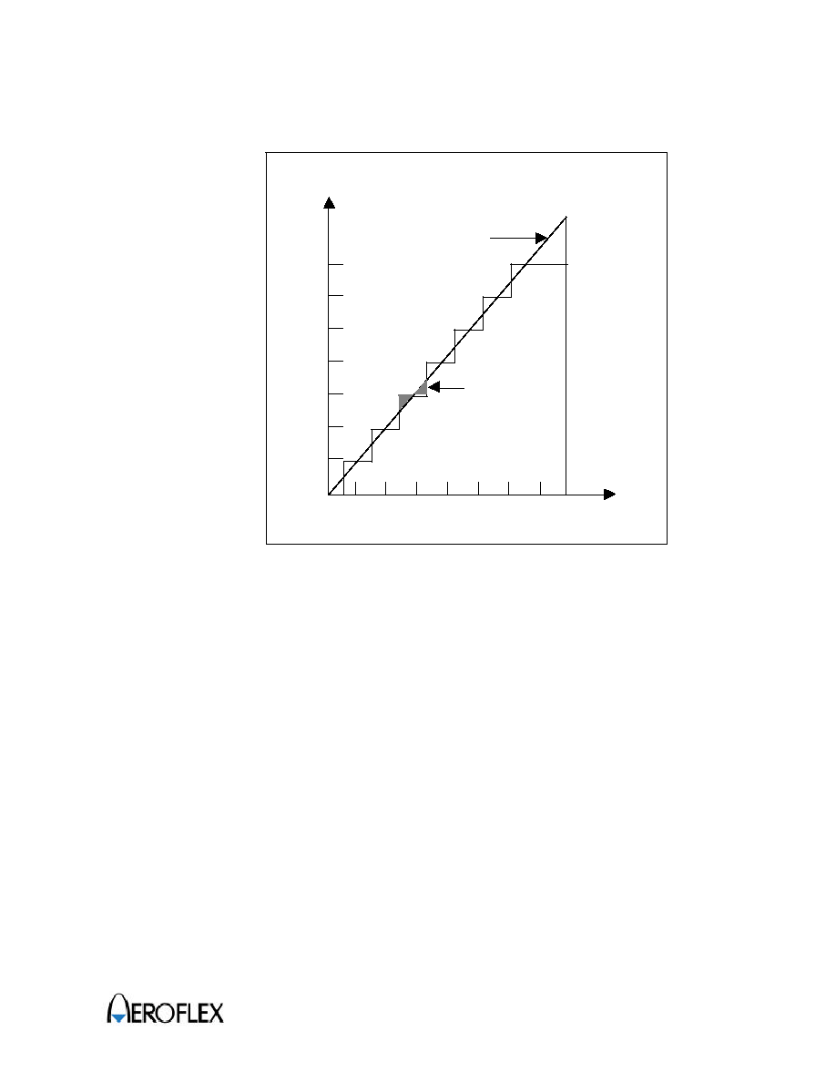
Chapter 13
AX07CF192
184
Figure 13.5 A/D Converter Accuracy Definitions (2)
7. Effect on Absolute Accuracy: Attaching an external capacitor creates a coupling with
ground, so if there is noise on the ground line, it may degrade absolute accuracy. The
capacitor must be connected to an electrically stable ground, such as AVSS.
If a filter circuit is used, be careful of interference with digital signals on the same board, and
make sure the circuit does not act as an antenna.
FS
Digital
Output
Analog Input
voltage
1/8 2/8
3/8
4/8
5/8
6/8
7/8
000
001
010
011
100
101
110
111
Ideal A/D conversion
characteristic
Quantization
error

Chapter 13
AX07CF192
185
13.6
Example
AREA
ADDONE, CODE, READONLY
ENTRY
ldr
r0, =ADC_base
; Make AOPSTOP to LOW to release power down mode,
add
r0, r0, #ADCCR
; then set normal operation mode.
mov
r1, #0
str
r1, [r0]
loop
; Check whether CALEND is set to 1 or not.
ldr
r2, [r0]
; (Check it's in the range of calibration time)
cmp
r2, #2
bne
loop
ldr
r0, =ADC_base
; Set the control bit in ADCSR register
add
r0, r0, #ADCSR
; AD conversion start, CKS=1/8 ADCLK, ACH=0ch
mov
r1, #0x40
;(set ADST, CKS=0, ACH=0)
str
r1, [r0]
loop_adf
;check ADF (AD conversion END)
adr
r2, [r0]
and
r2, r2, #0x80
cmp
r2, #0x80
bne
loop_adf
ldr
r1, [r0]
and
r1, r1, #0x7f ; Clear ADF to 0
str
r1, [r0]
ldr
r0, =ADC_base
;read ADDR0 register into R1 register
add
r0, r0, #ADDR0
ldr
r1, [r0]
END

Chapter 14
AX07CF192
186
Chapter 14
Electrical Characteristics

Chapter 14
AX07CF192
187
14.1
Absolute Maximum Ratings
Table 14.1 lists the absolute maximum ratings(Note1 and 2).
Table 14.1 Absolute Maximum Ratings
Item
Symbol
Value
Power supply voltage
V
DD
-0.5V to 4.6V
DC Input Voltage (except I/O pins)
V
IN
-0.5V to 6.0V
DC Output Voltage (Output in high or low state)
V
OUT
-0.5V to V
DD
+0.5V
DC Output Voltage (Output in 3-state)
V
OUT
-0.5V to +6.0V
Reference Voltage
V
REF
-0.3V to AV
DD
+0.3
Analog Power supply voltage
AV
CC
-0.3V to 3.6V
Analog Input Voltage
V
AN
-0.3V to AV
DD
+0.3
Storage Temperature range
T
S
-65 to +150�C
Note1: Absolute maximum continuous ratings are those values which damage to the device
may occur. Exposure to these conditions or conditions beyond those indicated may
adversely affect device reliability. Functional operation under absolute-maximum-
rated conditions is not implied.
Note2: Under transient conditions these ratings may be exceeded as elsewhere in this
specification.
14.2
Recommended Operating Conditions:
Table 14.2 lists the recommended operating conditions.
Table 14.2 Recommended Operating Conditions
Symbol
Parameter
MIN
MAX
UNIT
V
DD
Supply voltage
3.0
3.6
V
V
IN
Input voltage
0
5.5
V
V
OUT
Output voltage outputs active
0
V
DD
V
V
OUT
Output voltage outputs disabled
0
5.5
V
V
PPD
Flash program/erase voltage
4.5
5.5
V
T
A
Operating free-air temperature
-40
85
�C

Chapter 14
AX07CF192
188
14.3
DC Characteristics
Table 14.3 lists the DC characteristics .
Table 14.3 DC Characteristics
ITEM
SYM
BOL
MIN
MAX
UNIT
TEST Conditions
Input Low Voltage
V
IL
-0.5
0.3XV
DD
V
VDD=3.0V to 3.6V
Input High Voltage
V
IH
0.7XV
DD
V
DD
+0.5
V
VDD=3.0V to 3.6V
Output Low Voltage
V
OL
-
0.4
V
VDD=3.0V
I
OL
=0.8mA
Output High
Voltage
V
OH
2.4
-
V
VDD=3.0V
I
OH
=-0.8mA
Input current at
maximum voltage
I
I
-
1
mA
VDD=3.0V to 3.6V
Input=5.5V
Table 14.4 lists the IO circuit with pull-ups
Table 14.4 IO Circuits with pull-ups
Min Current(at PAD = 0V)
Max Current (at PAD = 0V)
3.3V Pull-up
30uA
-146uA
Equivalent
resistance
88.3kOhms
24.7kOhms
Table 14.5 lists the IO circuit with pull-downs
Table 14.5 IO Circuits with pull-downs
Min Current(at PAD =
2.65V)
Max Current (at PAD = 3.6V)
Pull-down
31uA
159uA
Equivalent
resistance
85.5kOhms
22.6kOhms

Chapter 14
AX07CF192
189
14.4
AC Characteristics
Timing measurement conditions is following that unless otherwise specified:
VDD: 3.3V
Junction Temperature: 25 �C
Process: Typical
Low-voltage input signal rising and falling edges switching time: 0.3ns
Clock timing parameters are listed in Table 14.6, control signal timing parameters in Table
14.7, and bus timing parameters in Table 14.8.
Table 14.6 Clock Timing
Item
Symbol
Min.
Max.
Units
Test
Conditions
Clock cycle time
t
CYC
20
1000
ns
Clock pulse low width
t
CL
10
-
ns
Clock pulse high width
t
CH
10
-
ns
Clock rise time
t
Cr
-
10
ns
Clock fall time
t
Cf
-
10
ns
Figure 14.3
Clock oscillator
Settling time at reset
t
OSC1
20
-
ms
Figure 14.1
Table 14.7 Control Signal Timing
Item
Symbol
Min.
Max.
Units
Test
Conditions
nRES setup time
t
RESS
200
-
ns
nRES pulse width
t
RESW
5
-
t
CYC
Mode programming
setup time
t
MDS
200
-
ns
Figure 14.2

Chapter 14
AX07CF192
190
Table 14.8 Bus Timing
(units: ns)
Item
Symbol
Min.
Max.
Test
Conditions
Address delay time
t
AD
-
20
Address hold time
t
AH
0
-
Read strobe delay time
t
RSD
-
20
Address strobe delay time
t
ASD
-
20
Write strobe delay time
t
WSD
-
20
Strobe delay time
t
SD
-
20
Write strobe pulse width 1
t
WSW1
20
-
Address setup time 1
t
AS1
10
-
Read data setup time
t
RDS
20
-
Read data hold time
t
RDH
0
-
Write data delay time
t
WDD
-
20
Write data setup time 1
t
WDS1
10
-
Write data hold time
t
WDH
0
-
Read data access time 1
t
ACC1
-
40
Read data access time 3
t
ACC3
-
40
Figure 14.3
Figure 14.4
Precharge time 1
t
PCH1
20
-
Precharge time 2
t
PCH2
0
-
Wait setup time
t
WTS
20
-
Wait hold time
t
WTH
5
-
Figure 14.5
Bus request setup time
t
BRQS
20
-
Bus acknowledge time 1
t
BACD1
-
30
Bus acknowledge time 2
t
BACD2
-
30
Bus-floating time
t
BZD
-
30
Figure 14.6

Chapter 14
AX07CF192
191
14.4
AD Conversion characteristics (Preliminary)
Table 14.9 lists the operation conditions of the AD Conversion
Table 14.9 Operating Conditions of the AD Conversion
Parameter
Symbol
Min.
Max.
Units
Power Supply
AVDD
3.0
3.6
V
Analog Input
AN
GND+0.2
AVREF-0.2
V
Clock Pulse Width
T
PWL
62.5
ns
Operating
Temperature
T
OP
-40
85
�C
Table 14.10 lists the electrical characteristics of the AD converter
Table 14.10 Electrical characteristics of the AD converter
Conditions : Analog input frequency F
IN
=1.26KHz, ADCLK=7.5MHz,
AV
DD
=DV
DD
=AV
REF
=3.3V T=25�C
Symbol
Parameter
Conditions
Min.
Typ.
Max.
Units
I
DD
Normal
ADCLK=7.5MHz
Input=AV
REF
F
IN
=1.26KHz ramp
2.0
mA
Power Down
ADCLK=7.5MHz
50
uA
AN
Analog input
voltage
GND+
0.2
AV
REF
-0.2
V
Accuracy
Resolution
10
bits
INL
Integral Non-
linearity
ADCLK=7.5MHz
Input=0-AVREF(V)
(F
IN
=1.26KHz)
�
2.0
LSB
DNL
Differential Non-
linearity
ADCLK=7.5MHz
Input=0-AV
REF
(F
IN
=1.26KHz ramp)
�
1.0
LSB
SNR
Signal-to-Noise
Ratio
Fsample=500Ksps,
F
IN
=1.26KHz
48
54
dB
SNDR
Signal-to-Noise
Distortion Ratio
45
54
dB
ADCLK
2
4
8
MHz
t
c
Conversion time
2
4
8
us
C
o
Output
capacitance
20
pF
Rref
Reference
resistance
10K
O
AV
REF
Analog
Reference
Voltage
AV
DD
V
T
CAL
Power up time
Calibration time
22
ms
THD
Total harmonic
distortion
55
60
dB
AVDD
Analog power
3.0
3.3
3.6
V
DVDD
Digital power
3.0
3.3
3.6
V
F
IN
Analog input
frequency
5
KHz

Chapter 14
AX07CF192
192
14.5
Operational Timing
14.5.1 Clock Timing
Figure. 14.1 shows the settling time of the crystal oscillator.
Figure 14.1 The settling time of the crystal oscillator
14.5.2 Reset Timing
Figure 14.2 show the reset input timing and reset output timing.
Figure 14.2 Reset Input Timing
XTALIN
VCC
XnRES
XnSTBY
t
OSC1
XTALIN
XnRES
MD
2
to MD
0
t
MDS
t
RESS
t
RESS
t
RESW

Chapter 14
AX07CF192
193
14.5.3 Bus Timing
Figure 14.3 and Figure 14.6 show the timing diagram of the bus controller.
Figure 14.3 The Write Timing Diagram of the Bus Controller
Figure 14.4 The Read Timing Diagram of the Bus Controller
XTALIN
A
23
to A
0
nCS
n
nAS
nRD
Data
(read)
t
CH
t
AD
t
CL
t
CYC
T1
T2
t
Cf
t
Cr
t
RDH
t
ACC3
t
AS1
t
SD
t
PCH1
t
CYC
t
AS1
t
ASD
t
ACC1
t
RSD
t
PCH2
t
ASD
t
ACC3
XTALIN
A
23
to A
0
nCS
n
nAS
nHWR, nLWR
Data
(write)
t
CH
t
AD
t
CL
t
CYC
T1
T2
t
Cf
t
Cr
t
AH
t
SD
t
PCH1
t
WDH
t
WDD
t
WDS1
t
AS1
t
ASD
t
WSW1
t
AS1
t
SD
t
PCH1
t
CYC
t
ASD

Chapter 14
AX07CF192
194
Figure 14.5 Basic Bus Cycle with External Wait State
Figure 14.6 Bus Release Mode Timing
XIN
nCS
n
Address
nAS
Data
(Read)
nHWR
nLWR
nRD
n
`1'
`1'
Valid
nWAIT
T1
T2
Tw
Tw
Tw
T3
t
WTS
t
WTH
XIN
Address
nBREQ
nBACK
t
BACD2
t
BRQS
t
BACD1
t
BRQS
t
BZD
t
BZD