
Advanced Monolithic Systems, Inc. 6680B Sierra Lane, Dublin, CA 94568 Phone (925) 556-9090 Fax (925) 556-9140
Advanced
AMS36063
Monolithic
DC-TO-DC CONVERTER CONTROL CIRCUIT
Systems
PRELIMINARY INFORMATION
FEATURES
APPLICATIONS
·
·
Wide Input Voltage Operating Range from 2.5V to 60V
·
·
Step-Up Converter
·
·
Low Standby Current
·
·
Step-Down Converter
·
·
Current Limiting
·
·
Voltage Inverting Application
·
·
Output Switch Current of 1.5A
·
·
Telephone Circuits
·
·
Output Voltage Adjustable from 1.25 to 40V
·
·
Monitors
·
·
Frequency of Operation to 100kHz
·
·
Battery Chargers
·
·
Thermal Protection
·
·
Portable Equipment
·
·
Enable Input Pin
GENERAL DESCRIPTION
The AMS36063 series is a control circuit containing the basic functions required for DC-to-DC converters. The device consists
of an internal temperature compensated reference, a comparator, a controlled duty cycle oscillator with an active current limit
circuit, a driver, a high current output switch, a thermal protection circuit and a converter enable input. Designed specifically to
be incorporated in Step-Up, Step-Down and Voltage -Inverting applications, the AMS36063 requires a minimum number of
external components.
The AMS36063 is available in the 8-lead plastic SOIC and 8-lead plastic DIP packages.
ORDERING INFORMATION
PACKAGE TYPE
OPER. TEMP
8 LEAD PDIP
8 LEAD SOIC
RANGE
AMS36063P
AMS36063S
-40
°
C to +85
°
C
PIN CONNECTIONS
8 LEAD SOIC/ 8 LEAD PDIP
Top View
COMPARATOR
INVERTING
INPUT
SWITCH
COLLECTOR
GND
ENABLE
TIMING
CAPACITOR
V
CC
I
PK
SENSE
SWITCH
EMITTER
1
2
8
4
3
7
5
6

Advanced Monolithic Systems, Inc. 6680B Sierra Lane, Dublin, CA 94568 Phone (925) 556-9090 Fax (925) 556-9140
AMS36063
ABSOLUTE MAXIMUM RATINGS
(Note 1)
Power Supply Voltage, V
CC
60V
Driver Collector Voltage, V
C(driver)
60V
Comparator Input Voltage Range, V
IR
-0.3V to
+60V
Switch Current, I
SW
1.5A
Switch Collector Voltage, V
C(switch)
60V
Power Dissipation
(Note 3)
Switch Emitter Voltage, V
E(switch)
60V
Maximum Junction Temperature
+125
°
C
Switch Collector to Emitter Voltage, V
CE(switch)
60V
Storage Temperature
-65
°
C to +150
°
C
ELECTRICAL CHARACTERISTICS
Electrical Characteristics at V
CC
= 5.0V, -40
°
C
T
A
+85
°
C, unless otherwise noted.
PARAMETER
CONDITIONS
Min.
AMS36063
Typ.
Max.
Units
Oscillator
Charging Current
5.0V
V
CC
60V, T
A
= 25
°
C
20
35
50
µ
A
Discharge Current
5.0V
V
CC
60V, T
A
= 25
°
C
150
200
250
µ
A
Voltage Swing
T
A
= 25
°
C
0.5
V
P-P
Discharge to Charge Current
Ratio
I
PK(sense)
= V
CC
, T
A
= 25
°
C
6.0
_
Current Limit Sense Voltage
I
CHG
= I
DISCHG
, T
A
= 25
°
C
250
300
350
mV
Output Switch (Note 2)
Saturation Voltage, Darlington
Connection
I
SW
= 1.0A, V
C(driver)
= V
C(switch)
1.0
1.3
V
Saturation Voltage
I
SW
= 1.0A, I
C(driver)
= 50mA, (Forced
20)
0.45
0.7
V
DC Current Gain
I
SW
= 1.0A, V
CE
= 5.0V, T
A
= 25
°
C
35
120
Collector Off-State Current
V
CE
= 60V, T
A
= 25
°
C
10
nA
Comparator
Threshold Voltage
1.18
1.25
1.32
V
Threshold Voltage Line
Regulation
3.0V
V
CC
60V
0.04
0.2
mV/V
Input Bias Current
V
IN
= 0V
40
400
nA
Total Device
ENABLE Low
3.0V
V
CC
60V
2.15
1.90
V
ENABLE Low
3.0V
V
CC
60V
2.50
2.26
V
Supply Current
5.0V
V
CC
60V, I
PK(sense)
= V
CC
,
C
T
= 0.001
µ
F, V pin 5 > V
th
,
Pin 2 = Gnd, Remaining pins open
2.4
4.0
mA
Note 1: Absolute Maximum Ratings are limits beyond which damage to the device may occur. For guaranteed performance limits and associated test
conditions, see the Electrical Characteristics tables.
Note 2: To minimize power dissipation, low duty cycle pulse testing is used.
Note 3: Power dissipation at T
A
= 25
°
C is equal to 1.0W for the 8 lead P DIP package and 625mW for the SO-8 package. For operation at temperatures above
T
A
= 25
°
C derate the power dissipation at 10mW/
°
C.

Advanced Monolithic Systems, Inc. 6680B Sierra Lane, Dublin, CA 94568 Phone (925) 556-9090 Fax (925) 556-9140
AMS36063
FUNCTIONAL BLOCK DIAGRAM
TYPICAL PERFORMANCE CHARACTERISTICS
OSCILLATOR TIMING CAPACITOR
OUTPUT SWITCH ON-OFF TIME (
µ
s)
1.0
1000
Output Switch On-Off Time vs
Oscillator Timing Capacitor
10
10
100
0.1
1.0
100
0
0.8
3.2
0
5.0 10
20
30
40
50
60
SUPPLY VOLTAGE (V)
Standby Supply Current vs
Supply Voltage
SUPPLY CURRENT (mA)
1.6
2.4
V
CC
= 5.0V
I
PK(sense)
= V
CC
Pin 5 = GND
Emitter-Follower Configuration
Output Switch Saturation Voltage
vs Emitter Current
EMITTER CURRENT (A)
SATURATION VOLTAGE (V)
0
0.2 0.4 0.6
0.8
1.0
1.0
1.1
1.2
1.3
1.4
1.5
1.6
1.2 1.4
V
CC
= 5.0V
Pins 1,7 = V
CC
Pin 3,5 = GND
Common-Emitter Configuration
Output Switch Saturation Voltage
vs Collector Current
COLLECTOR CURRENT (A)
SATURATION VOLTAGE (V)
0
0.2 0.4 0.6
0.8
1.0
0
0.2
0.4
0.6
0.8
1.0
1.2
1.2 1.4
V
CC
= 5.0V
Pin 7 = V
CC
Pin 2,3,5 = GND
Darlington Connection
Forced Beta
20
C
T
= 0.001
µ
F
I
PK(sense)
= V
CC
Pin 2 = GND
1.25V
REF
REG
8
7
6
5
+
-
4
1
2
3
COMP.
I
PK
C
T
OSC
R
S
Q
Q
2
Q
1
170
SWITCH
COLLECTOR
SWITCH
EMITTER
TIMING
CAPACITOR
GND
ENABLE
I
PK
SENSE
V
CC
COMPARATOR
INVERTING
INPUT
180
Advanced Monolithic Systems, Inc. 6680B Sierra Lane, Dublin, CA 94568 Phone (925) 556-9090 Fax (925) 556-9140
AMS36063
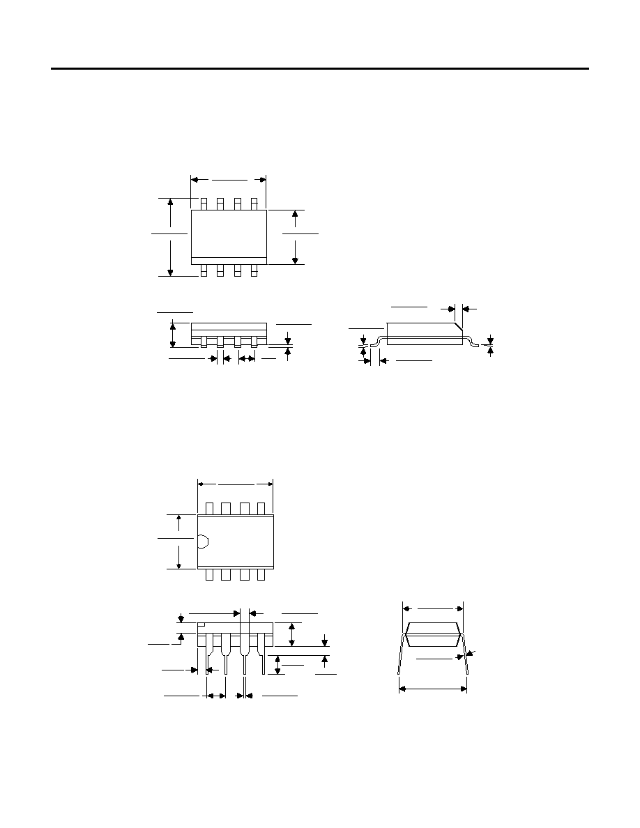
PACKAGE DIMENSIONS inches (millimeters) unless otherwise noted.
8 LEAD SOIC PLASTIC PACKAGE (S)
8 LEAD PLASTIC DIP PACKAGE (P)
0°-8° TYP
0.010-0.020
(0.254-0.508)
S (SO-8 ) AMS DRW# 042293
x 45°
0.016-0.050
(0.406-1.270)
0.008-0.010
(0.203-0.254)
0.004-0.010
(0.101-0.254)
0.014-0.019
(0.355-0.483)
0.053-0.069
(1.346-1.752)
0.050
(1.270)
TYP
0.150-0.157**
(3.810-3.988)
0.228-0.244
(5.791-6.197)
0.189-0.197*
(4.801-5.004)
*DIMENSION DOES NOT INCLUDE MOLD FLASH. MOLD FLASH
SHALL NOT EXCEED 0.006" (0.152mm) PER SIDE
**DIMENSION DOES NOT INCLUDE INTERLEAD FLASH. INTERLEAD
FLASH SHALL NOT EXCEED 0.010" (0.254mm) PER SIDE
1
2
3
4
8
7
6
5
0.045-0.065
(1.143-1.651)
0.255±0.015*
(6.477±0.381)
0.400*
(10.160)
MAX
1
2
3
4
8
7
6
5
0.130±0.005
(3.302±0.127)
0.018±0.003
(0.457±0.076)
0.100±0.010
(2.540±0.254)
(
8.255
)
+0.635
-0.381
0.325 +0.025
-0.015
0.009-0.015
(0.229-0.381)
0.300-0.325
(7.620-8.255)
0.065
(1.651)
TYP
0.005
(0.127)
MIN
0.125
(3.175)
MIN
0.015
(0.380)
MIN
*DIMENSIONS DO NOT INCLUDE MOLD FLASH OR PROTUSIONS.
MOLD FLASH OR PROTUSIONS SHALL NOT EXCEED 0.010" (0.254mm)
P (8L PDIP ) AMS DRW# 042294