Äîêóìåíòàöèÿ è îïèñàíèÿ www.docs.chipfind.ru
REV. 0
Information furnished by Analog Devices is believed to be accurate and
reliable. However, no responsibility is assumed by Analog Devices for its
use, nor for any infringements of patents or other rights of third parties
which may result from its use. No license is granted by implication or
otherwise under any patent or patent rights of Analog Devices.
a
Airflow and Temperature Sensor
TMP12*
© Analog Devices, Inc., 1995
One Technology Way, P.O. Box 9106, Norwood. MA 02062-9106, U.S.A.
Tel: 617/329-4700
Fax: 617/326-8703
FEATURES
Temperature Sensor Includes 100
Heater
Heater Provides Power IC Emulation
Accuracy 3
°
C typ. from 40
°
C to 100
°
C
Operation to 150
°
C
5 mV/
°
C Internal Scale-Factor
Resistor Programmable Temperature Setpoints
20 mA Open-Collector Setpoint Outputs
Programmable Thermal Hysteresis
Internal 2.5 V Reference
Single 5 V Operation
400
µ
A Quiescent Current (Heater OFF)
Minimal External Components
APPLICATIONS
System Airflow Sensor
Equipment Over-Temperature Sensor
Over-Temperature Protection
Power Supply Thermal Sensor
Low-Cost Fan Controller
GENERAL DESCRIPTION
The TMP12 is a silicon-based airflow and temperature sensor
designed to be placed in the same airstream as heat generating
components that require cooling. Fan cooling may be required
continuously, or during peak power demands, e.g. for a power
supply, and if the cooling systems fails, system reliability and/or
safety may be impaired. By monitoring temperature while emu-
lating a power IC, the TMP12 can provide a warning of cooling
system failure.
The TMP12 generates an internal voltage that is linearly pro-
portional to Celsius (Centigrade) temperature, nominally
5 mV/
°
C. The linearized output is compared with voltages
from an external resistive divider connected to the TMP12's
2.5 V precision reference. The divider sets up one or two refer-
ence voltages, as required by the user, providing one or two
temperature setpoints. Comparator outputs are open-collector
transistors able to sink over 20 mA. There is an on-board hys-
teresis generator provided to speed up the temperature-setpoint
output transitions, this also reduces erratic output transitions in
noisy environments. Hysteresis is programmed by the external
resistor chain and is determined by the total current drawn from
the 2.5 V reference. The TMP12 airflow sensor also incorpo-
rates a precision, low temperature coefficient 100
heater
resistor that may be connected directly to an external 5 V sup-
ply. When the heater is activated it raises the die temperature in
the DIP package approximately 20
°
C above ambient (in still
air). The purpose of the heater in the TMP12 is to emulate a
power IC, such as a regulator or Pentium CPU which has a high
internal dissipation.
When subjected to a fast airflow, the package and die tempera-
tures of the power device and the TMP12 (if located in the
same airstream) will be reduced by an amount proportional to
the rate of airflow. The internal temperature rise of the TMP12
may be reduced by placing a resistor in series with the heater, or
reducing the heater voltage.
The TMP12 is intended for single 5 V supply operation, but will
operate on a 12 V supply. The heater is designed to operate from
5 V only. Specified temperature range is from 40
°
C to 125
°
C,
operation extends to 150
°
C at 5 V with reduced accuracy.
The TMP12 is available in 8-pin plastic DIP and SO packages.
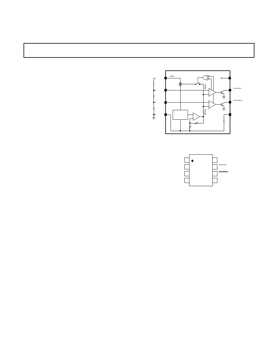
FUNCTIONAL BLOCK DIAGRAM
VREF
OVER
1k
+
-
V+
GND
SET
HIGH
HEATER
HYSTERESIS
VOLTAGE
WINDOW
COMPARATOR
CURRENT
MIRROR
HYSTERESIS
CURRENT
VOLTAGE
REFERENCE
AND
SENSOR
IHYS
+
-
+
-
UNDER
SET
LOW
100
PINOUTS
DIP And SO
TOP VIEW
(Not to Scale)
8
V+
1
VREF
7
OVER
2
SET HIGH
6
UNDER
SET LOW
3
5
HEATER
GND
4
*Protected by U.S. Patent No. 5,195,827.

Parameter
Symbol
Conditions
Min
Typ
Max
Units
ACCURACY
Accuracy (High, Low Setpoints)
T
A
= 25
°
C
2
3
°
C
Accuracy (High, Low Setpoints)
T
A
= 40
°
C to 100
°
C
3
5
°
C
Internal Scale Factor
T
A
= 40
°
C to 100
°
C
4.9
5
5.1
mV/
°
C
Power Supply Rejection Ratio
PSRR
4.5 V
V
S
5.5 V
0.1
0.5
°
C/V
Linearity
T
A
= 40
°
C to 125
°
C
0.5
°
C
Repeatability
T
A
= 40
°
C to 125
°
C
0.3
°
C
Long Term Stability
T
A
= 125
°
C for 1 k Hrs
0.3
°
C
SETPOINT INPUTS
Offset Voltage
V
OS
0.25
mV
Output Voltage Drift
TCV
OS
3
µ
V/
°
C
Input Bias Current
I
B
25
100
nA
VREF OUTPUT
Output Voltage
VREF
T
A
= 25
°
C, No Load
2.49
2.50
2.51
V
Output Voltage
VREF
T
A
= 40
°
C to 100
°
C,
2.5 0.015
V
No Load
Output Drift
TC
VREF
10
ppm/
°
C
Output Current, Zero Hysteresis
I
VREF
7
µ
A
Hysteresis Current Scale Factor
SF
HYS
5
µ
A/
°
C
OPEN-COLLECTOR OUTPUTS
Output Low Voltage
V
OL
I
SINK
= 1.6 mA
0.25
0.4
V
Output Low Voltage
V
OL
I
SINK
= 20 mA
0.6
V
Output Leakage Current
I
OH
V
S
= 12 V
1
100
µ
A
Fall Time
t
HL
See Test Load
40
ns
HEATER
Resistance
R
H
T
A
= 25
°
C
97
100
103
Temperature Coefficient
T
A
= 40
°
C to 125
°
C
100
ppm/
°
C
Maximum Continuous Current
I
H
See Note 1
60
mA
POWER SUPPLY
Supply Range
V
S
4.5
5.5
V
Supply Current
I
SY
Unloaded at 5 V
400
600
µ
A
I
SY
Unloaded at 12 V
2
450
µ
A
NOTES
1
Guaranteed but not tested.
2
TMP12 is specified for operation from a 5 V supply. However, operation is allowed up to a 12 V supply, but not tested at 12 V. Maximum heater supply is 6 V.
Specifications subject to change without notice.
TMP12SPECIFICATIONS
REV. 0
2
(V
S
= 5 V, 40
°
C
T
A
125
°
C unless otherwise noted.)
20pF
1k
TEST LOAD
CAUTION
ESD (electrostatic discharge) sensitive device. Electrostatic charges as high as 4000 V readily
accumulate on the human body and test equipment and can discharge without detection.
Although the TMP12 features proprietary ESD protection circuitry, permanent damage may
occur on devices subjected to high energy electrostatic discharges. Therefore, proper ESD
precautions are recommended to avoid performance degradation or loss of functionality.
TMP12
REV. 0
3
Parameter
Symbol
Conditions
Min
Typ
Max
Units
ACCURACY
Accuracy (High, Low Setpoints)
T
A
= 25
°
C
3
°
C
Internal Scale Factor
T
A
= 25
°
C
4.9
5
5.1
mV/
°
C
SETPOINT INPUTS
Input Bias Current
I
B
100
nA
VREF OUTPUT
Output Voltage
VREF
T
A
= 25
°
C, No Load
2.49
2.51
V
OPEN-COLLECTOR OUTPUTS
Output Low Voltage
V
OL
I
SINK
= 1.6 mA
0.4
V
Output Leakage Current
I
OH
V
S
= 12 V
100
µ
A
HEATER
Resistance
R
H
T
A
= 25
°
C
97
100
103
POWER SUPPLY
Supply Range
V
S
4.5
5.5
V
Supply Current
I
SY
Unloaded at 5 V
600
µ
A
NOTE
Electrical tests are performed at wafer probe to the limits shown. Due to variations in assembly methods and normal yield loss, yield after packaging is not guaranteed
for standard product dice. Consult factory to negotiate specifications based on dice lot qualification through sample lot assembly and testing.
DICE CHARACTERISTICS
Die Size 0.078 0.071 inch, 5,538 sq. mils
(1.98 1.80 mm, 3.57 sq. mm)
Transistor Count: 105
WAFER TEST LIMITS
(V
S
= 5 V, GND = O V, T
A
= 25
°
C, unless otherwise noted.)
1. VREF
2. SET HIGH INPUT
3. SET LOW INPUT
4. GND
5. HEATER
6. UNDER OUTPUT
7. OVER OUTPUT
8. V
For additional DICE ordering information, refer to databook.
8
3
7
5
4
1
2
WARNING!
ESD SENSITIVE DEVICE
6

TMP12
REV. 0
4
ABSOLUTE MAXIMUM RATINGS*
Supply Voltage . . . . . . . . . . . . . . . . . . . . . . . .
0.3 V to 15 V
Heater Voltage . . . . . . . . . . . . . . . . . . . . . . . . . . . . . . . . .
6 V
Setpoint Input Voltage . . . . . . . . . . .
0.3 V to [(V ) 0.3 V]
Reference Output Current . . . . . . . . . . . . . . . . . . . . . . . . 2 mA
Open-Collector Output Current . . . . . . . . . . . . . . . . . . 50 mA
Open-Collector Output Voltage . . . . . . . . . . . . . . . . . . .
15 V
Operating Temperature Range . . . . . . . . . .
55
°
C to 150
°
C
Dice Junction Temperature . . . . . . . . . . . . . . . . . . . . .
175
°
C
Storage Temperature Range . . . . . . . . . . . .
65
°
C to 160
°
C
Lead Temperature(Soldering, 60 sec) . . . . . . . . . . . . .
300
°
C
Package Type
JA
JC
Units
8-Pin Plastic DIP (P)
103
1
43
°
C/W
8-Lead SOIC (S)
158
2
43
°
C/W
NOTES
1
JA is specified for device in socket (worst case conditions).
2
JA is specified for device mounted on PCB.
CAUTION
1. Stresses above those listed under "Absolute Maximum
Ratings" may cause permanent damage to the device. This is a
stress rating only and functional operation at or above this
specification is not implied. Exposure to the above maximum
rating conditions for extended periods may affect device reli-
ability.
2. Digital inputs and outputs are protected, however, permanent
damage may occur on unprotected units from high-energy
electrostatic fields. Keep units in conductive foam or packaging
at all times until ready to use. Use proper antistatic handling
procedures.
3. Remove power before inserting or removing units from their
sockets.
ORDERING GUIDE
Temperature
Package
Package
Model/Grade
Range
1
Description
Option
TMP12FP
XIND
Plastic DIP
N-8
TMP12FS
XIND
SOIC
SO-8
TMP12GBC
25
°
C
Die
NOTE
1
XIND = 40
°
C to 125
°
C
FUNCTIONAL DESCRIPTION
The TMP12 incorporates a heating element, temperature sen-
sor, and two user-selectable setpoint comparators on a single
substrate. By generating a known amount of heat, and using the
setpoint comparators to monitor the resulting temperature rise,
the TMP12 can indirectly monitor the performance of a
system's cooling fan.
The TMP12 temperature sensor section consists of a bandgap
voltage reference which provides both a constant 2.5 V output
and a voltage which is proportional to absolute temperature
(VPTAT). The VPTAT has a precise temperature coefficient of
5 mV/K and is 1.49 V (nominal) at 25
°
C. The comparators
compare VPTAT with the externally set temperature trip points
and generate an open-collector output signal when one of their
respective thresholds has been exceeded.
The heat source for the TMP12 is an on-chip 100
low
tempco thin-film resistor. When connected to a 5 V source, this
resistor dissipates:
PD =
V2
R
52 V
100
= 0.25 W ,
=
which generates a temperature rise of about 32
°
C in still air for
the SO packaged device. With an airflow of 450 feet per minute
(FPM), the temperature rise is about 22
°
C. By selecting a temp-
erature setpoint between these two values, the TMP12 can provide
a logic-level indication of problems in the cooling system.
A proprietary, low tempco thin-film resistor process, in conjunc-
tion with production laser trimming, enables the TMP12 to
provide a temperature accuracy of 3
°
C (typ) over the rated
temperature range. The open-collector outputs are capable of
sinking 20 mA, allowing the TMP12 to drive small control re-
lays directly. Operating from a single 5 V supply, the quiescent
current is only 600
µ
A (max), without the heater resistor current.
TMP12
REV. 0
5
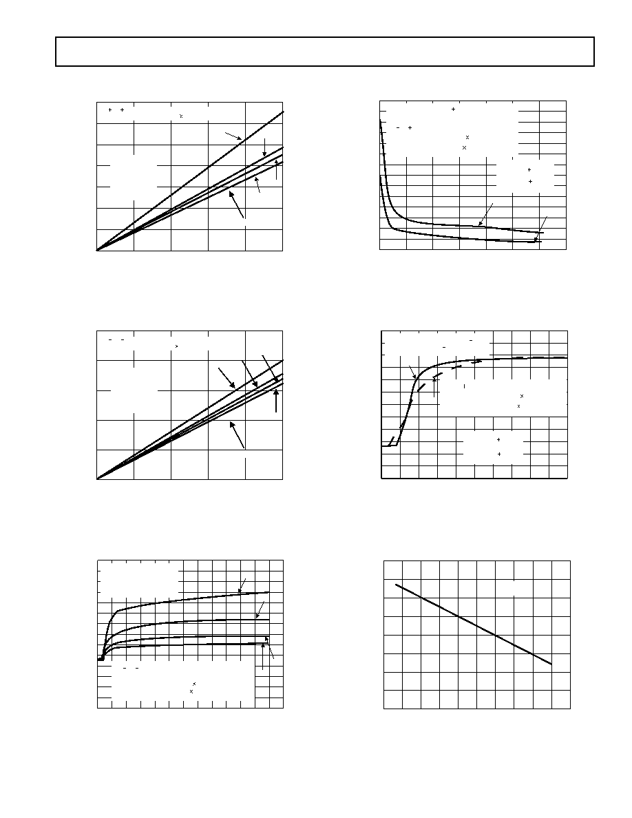
HEATER RESISTOR POWER DISSIPATION mW
35
30
0
0
50
100
150
200
20
15
10
5
25
AIR FLOW RATES
V = 5V
SO8 SOLDERED TO .5 " .3" Cu PCB
JUNCTION TEMPERATURE RISE ABOVE AMBIENT
°
C
250
a. 0 FPM
c. 450 FPM
b. 250 FPM
d. 600 FPM
a
b
c
d
Figure 1. SOIC Junction Temperature Rise vs. Heater
Dissipation
HEATER RESISTOR POWER DISSIPATION mW
JUNCTION TEMPERATURE RISE ABOVE AMBIENT
°
C 25
20
0
0
250
50
100
150
200
15
10
5
AIR FLOW RATES
V = 5V
PDIP SOLDERED TO 2" 1.31" Cu PCB
a. 0 FPM
c. 450 FPM
b. 250 FPM
d. 600 FPM
a
b
c
d
Figure 2. PDIP Junction Temperature Rise vs. Heater
Dissipation
TIME sec
25
20
0
15
10
5
30
35
40
45
50
55
60
65
70
0
10
20
30
40
50
60
70
80
90 100 110 120 130
V = 5V RHEATER TO EXTERNAL
SUPPLY TURNED ON @ t = 5 sec
SO8 SOLDERED TO .5" .3" COPPER PCB
PDIP SOLDERED TO 2" 1.31 COPPER PCB
a. SO8, HTR @ 5V
b. PDIP, HTR @ 5V
c. SO8, HTR @ 3V
d. PDIP, HTR @ 3V
a
b
c
d
JUNCTION TEMPERATURE
°
C
Figure 3. Junction Temperature Rise in Still Air
TRANSITION FROM 100
°
C STIRRED
BATH TO FORCED 25
°
C AIR
V = 5V, NO LOAD, HEATER OFF
SO8 SOLDERED TO .5" .3" Cu PCB
PDIP SOLDERED TO 2" 1.31" Cu PCB
AIR VELOCITY FPM
140
0
0
700
100
TIME CONSTANT sec
200
300
400
500
600
120
80
60
40
20
100
a. PDIP PCB
b. SOIC PCB
a
b
Figure 4. Package Thermal Time Constant in Forced Air
TIME sec
80
30
0
0
2
JUNCTION TEMPERATURE
°
C
4
6
8
10
12
14
16
18
20
70
40
20
10
60
50
90
100
110
120
V = 5V, NO LOAD, HEATER OFF
SO8 SOLDERED TO .5" .3" Cu PCB
PDIP SOLDERED TO 2" 1.31" Cu PCB
a. SO8 PCB
b. PDIP PCB
a
b
TRANSITION FROM STILL 25
°
C
AIR TO STIRRED 100
°
C BATH
Figure 5. Thermal Response Time in Stirred Oil Bath
TEMPERATURE
°
C
102
99.5
98
-75
HEATER RESISTANCE
-25
25
75
125
175
101.5
100
99
98.5
101
100.5
V+ = +5V
Figure 6. Heater Resistance vs. Temperature
TMP12
REV. 0
6
TEMPERATURE
°
C
2.52
2.505
2.49
-75
175
REFERENCE VOLTAGE V
-25
25
75
125
2.515
2.51
2.5
2.495
V = 5V, NO LOAD, HEATER OFF
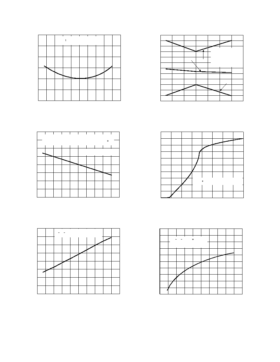
Figure 7. Reference Voltage vs. Temperature
TEMPERATURE
°
C
5
4
3
-75
175
START-UP SUPPLY VOLTAGE V
-25
25
75
125
4.5
3.5
START-UP VOLTAGE DEFINED AS OUTPUT
READING BEING WITHIN 5
°
C OF OUTPUT AT 5V
NO LOAD, HEATER OFF
Figure 8. Start-up Voltage vs. Temperature
TEMPERATURE
°
C
500
400
300
475
450
350
325
425
375
-75
175
SUPPLY CURRENT µA
-25
25
75
125
V = 5V, NO LOAD, HEATER OFF
Figure 9. Supply Current vs. Temperature
TEMPERATURE
°
C
-50
-25
25
75
125
ACCURACY ERROR
°
C
0
50
100
2
-3
1
-2
-4
-5
0
-1
3
4
5
6
-6
a. MAXIMUM LIMIT
c. MINIMUM LIMIT
b. ACCURACY ERROR
a
b
c
Figure 10. Accuracy Error vs. Temperature
SUPPLY VOLTAGE V
400
0
350
200
150
100
50
300
250
450
500
0
8
1
SUPPLY CURRENT µA
2
3
4
5
6
7
Ta = 25
°
C, NO LOAD, HEATER OFF
Figure 11. Supply Current vs. Supply Voltage
TEMPERATURE
°
C
0.4
0
-75
POWER SUPPLY REJECTION
°
C/V
-25
25
75
125
175
0.2
0.1
0.3
0.5
V = 4.5 TO 5.5V
NO LOAD, HEATER OFF
Figure 12. VPTAT Power Supply Rejection vs.
Temperature
TMP12
REV. 0
7
TEMPERATURE
°
C
36
20
-75
OPEN COLLECTOR SINK CURRENT mA
-25
25
75
125
175
28
24
32
40
VOL = 1V, V = 5V
22
38
34
30
26
Figure 13. Open-Collector Output Sink Current vs.
Temperature
TEMPERATURE
°
C
700
0
-75
175
OPENCOLLECTOR OUTPUT VOLTAGE mV
-25
25
75
125
600
500
400
300
200
100
a. LOAD = 10mA
c. LOAD = 1mA
b. LOAD = 5mA
a
b
c
V = 5V
Figure 14. Open-Collector Voltage vs. Temperature
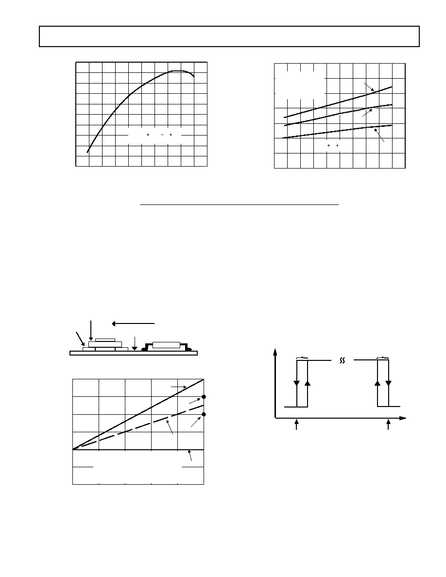
APPLICATIONS INFORMATION
A typical application for the TMP12 is shown in Figure 15. The
TMP12 package is placed in the same cooling airflow as a
high-power dissipation IC. The TMP12's internal resistor pro-
duces a temperature rise which is proportional to air flow, as
shown in Figure 16. Any interruption in the airflow will produce
an additional temperature rise. When the TMP12 chip tempera-
ture exceeds a user-defined setpoint limit, the system controller
can take corrective action, such as: reducing clock frequency,
shutting down unneeded peripherals, turning on additional fan
cooling, or shutting down the system.
POWER I.C.
PGA
PACKAGE
PGA
SOCKET
PC BOARD
AIR FLOW
TMP12
Figure 15. Typical Application
35
40
45
50
55
60
65
50
100
150
200
250
0
DIE TEMPERATURE (
°
C)
TMP12 P
D
(mW)
a. TMP12 DIE TEMP NO AIR FLOW
c. LOW SET POINT
b. HIGH SET POINT
d. TMP12 DIE TEMP MAX AIR FLOW
e. SYSTEM AMBIENT TEMPERATURE
a
b
c
d
e
Figure 16. Choosing Temperature Setpoints
Temperature Hysteresis
The temperature hysteresis at each setpoint is the number
of degrees beyond the original setpoint temperature that
must be sensed by the TMP12 before the setpoint compar-
ator will be reset and the output disabled. Hysteresis
prevents "chatter" and "motorboating" in feedback control
systems. For monitoring temperature in computer systems,
hysteresis prevents multiple interrupts to the CPU which
can reduce system performance.
Figure 17 shows the TMP12's hysteresis profile. The hyster-
esis is programmed, by the user, by setting a specific load
current on the reference voltage output VREF. This output
current, I
REF
, is also called the hysteresis current. I
REF
is mir-
rored internally by the TMP12, as shown in the functional
block diagram, and fed to a buffer with an analog switch.
LO
HI
OUTPUT
VOLTAGE
OVER, UNDER
TEMPERATURE
HYSTERESIS
LOW
HYSTERESIS HIGH =
HYSTERESIS LOW
T
SETLOW
T
SETHIGH
HYSTERESIS
HIGH
Figure 17. TMP12 Hysteresis Profile
After a temperature setpoint has been exceeded and a com-
parator tripped, the hysteresis buffer output is enabled. The
result is a current of the appropriate polarity which gener-
ates a hysteresis offset voltage across an internal 1 k
resistor at the comparator input. The comparator output
remains "on" until the voltage at the comparator input,
now equal to the temperature sensor voltage VPTAT
summed with the hysteresis effect, has returned to the pro-
grammed setpoint voltage. The comparator then returns
TMP12
REV. 0
8
LOW, deactivating the open-collector output and disabling the
hysteresis current buffer output. The scale factor for the pro-
grammed hysteresis current is:
I = I
VREF
= 5
µ
A/
°
C 7
µ
A
Thus, since VREF = 2.5 V, a reference load resistance of 357 k
or greater (output current of 7
µ
A or less) will produce a tem-
perature setpoint hysteresis of zero degrees. For more details, see
the temperature programming discussion below. Larger values of
load resistance will only decrease the output current below 7
µ
A,
but will have no effect on the operation of the device. The
amount of hysteresis is determined by selecting an appropriate
value of load resistance for VREF, as shown below.
Programming the TMP12
The basic thermal monitoring application only requires a simple
three-resistor ladder voltage divider to set the high and low
setpoints and the hysteresis. These resistors are programmed in
the following sequence:
1. Select the desired hysteresis temperature.
2. Calculate the hysteresis current, I
VREF
3. Select the desired setpoint temperatures.
4. Calculate the individual resistor divider ladder values needed
to develop the desired comparator setpoint voltages at the
Set High and Set Low inputs.
The hysteresis current is readily calculated, as shown above. For
example, to produce 2 degrees of hysteresis I
VREF
should be set
to 17
µ
A. Next, the setpoint voltages V
SETHIGH
and V
SETLOW
are
determined using the VPTAT scale factor of 5 mV/K = 5 mV/
(
°
C 273.15), which is 1.49 V for 25
°
C. Finally, the divider
resistors are calculated, based on the setpoint voltages.
The setpoint voltages are calculated from the equation:
V
SET
= (T
SET
273.15)(5 mV/
°
C)
This equation is used to calculate both the V
SETHIGH
and the
V
SETLOW
values. A simple 3-resistor network, as shown in Figure
18, determines the setpoints and hysteresis value. The equations
used to calculate the resistors are:
R1 (k
) = (V
REF
V
SETHIGH
)/I
VREF
= (2.5 V V
SETHIGH
)/I
VREF
R2 (k
) = (V
SETHIGH
V
SETLOW
)/I
VREF
R3 (k
) = V
SETLOW
/I
VREF
1
2
3
4
8
7
6
5
(
VREF
V
SETHIGH
) / I
VREF
= R1
TMP12
(V
SETHIGH
V
SETLOW
) / I
VREF
= R2
V
SETLOW
/ I
VREF
= R3
V
SETHIGH
V
SETLOW
VREF
= 2.5 V
I
VREF
GND
V+
HEATER
UNDER
OVER
Figure 18. TMP12 Setpoint Programming
For example, setting the high setpoint for 80
°
C, the low
setpoint for 55
°
C, and hysteresis for 3
°
C produces the
following values:
I
HYS
= I
VREF
= (3
°
C 5
µ
A/
°
C) 7
µ
A = 15
µ
A 7
µ
A =
22
µ
A
V
SETHIGH
= (T
SETHIGH
273.15)(5 mV/
°
C) = (80
°
C
273.15)(5 mV/
°
C) = 1.766 V
V
SETLOW
= (T
SETLOW
273.15)(5 mV/
°
C) = (55
°
C 273.15)
(5 mV/
°
C) = 1.641 V
R1 (k
) = (VREF V
SETHIGH
)/I
VREF
= (2.5 V 1.766 V)/
22
µ
A = 33.36 k
R2 (k
) = (V
SETHIGH
V
SETLOW
)/I
VREF
= (1.766 V 1.641 V)/
22
µ
A = 5.682 k
R3 (k
) = V
SETLOW
/ I
VREF
= (1.641 V)/22
µ
A = 74.59 k
The total of R1 R2 R3 is equal to the load resistance
needed to draw the desired hysteresis current from the
reference, or I
VREF
.
The nomograph of Figure 19 provides an easy method of
determining the correct VPTAT voltage for any temperature.
Simply locate the desired temperature on the appropriate scale
(K,
°
C or
°
F) and read the corresponding VPTAT value from
the bottom scale.
218
248
273
298
323
348
373
398
55
25 18
0
25
50
75
100
125
67
25
0
32 50
77
100
150
200 212
257
VPTAT
K
°
F
1.09
1.24
1.365
1.49
1.615
1.74
1.865
1.99
°C
Figure 19. Temperature VPTAT Scale
The formulas shown above are also helpful in understanding the
calculations of temperature setpoint voltages in circuits other
than the standard two-temperature thermal/airflow monitor. If a
setpoint function is not needed, the appropriate comparator in-
put should be disabled. SETHIGH can be disabled by tying it
to V or VREF, SETLOW by tying it to GND. Either output
can be left disconnected.
Selecting Setpoints
Choosing the temperature setpoints for a given system is an em-
pirical process, because of the wide variety of thermal issues in
any practical design. The specific setpoints are dependent on
such factors as airflow velocity in the system, adjacent compo-
nent location and size, PCB thickness, location of copper
ground planes, and thermal limits of the system.
The TMP12's temperature rise above ambient is proportional to
airflow (Figures 1, 2 and 16). As a starting point, the low
setpoint temperature could be set at the system ambient temp-
erature (inside the enclosure) plus one half of the temperature
rise above ambient (at the actual airflow in the system). With
this setting, the low limit will provide a warning either if the fan
output is reduced or if the ambient temperature rises (for ex-
ample, if the fan's cool air intake is blocked). The high setpoint
could then be set for the maximum system temperature to pro-
vide a final system shutdown control.
TMP12
REV. 0
9
Measuring the TMP12 Internal Temperature
As previously mentioned, the TMP12's VPTAT generator repre-
sents the chip temperature with a slope of 5 mV/K. In some cases,
selecting the setpoints is made easier if the TMP12's internal
VPTAT voltage (and therefore the chip temperature) is known.
For example, the case temperature of a high power microprocessor
can be monitored with a thermistor, thermocouple, or other mea-
surement method. The case temperature can then be correlated
with the TMP12's temperature to select the setpoints.
The TMP12's VPTAT voltage is not available externally, so indi-
rect methods must be used. Since the VPTAT voltage is applied to
the internal comparators, measuring the voltage at which the digital
output changes state will reflect the VPTAT voltage.
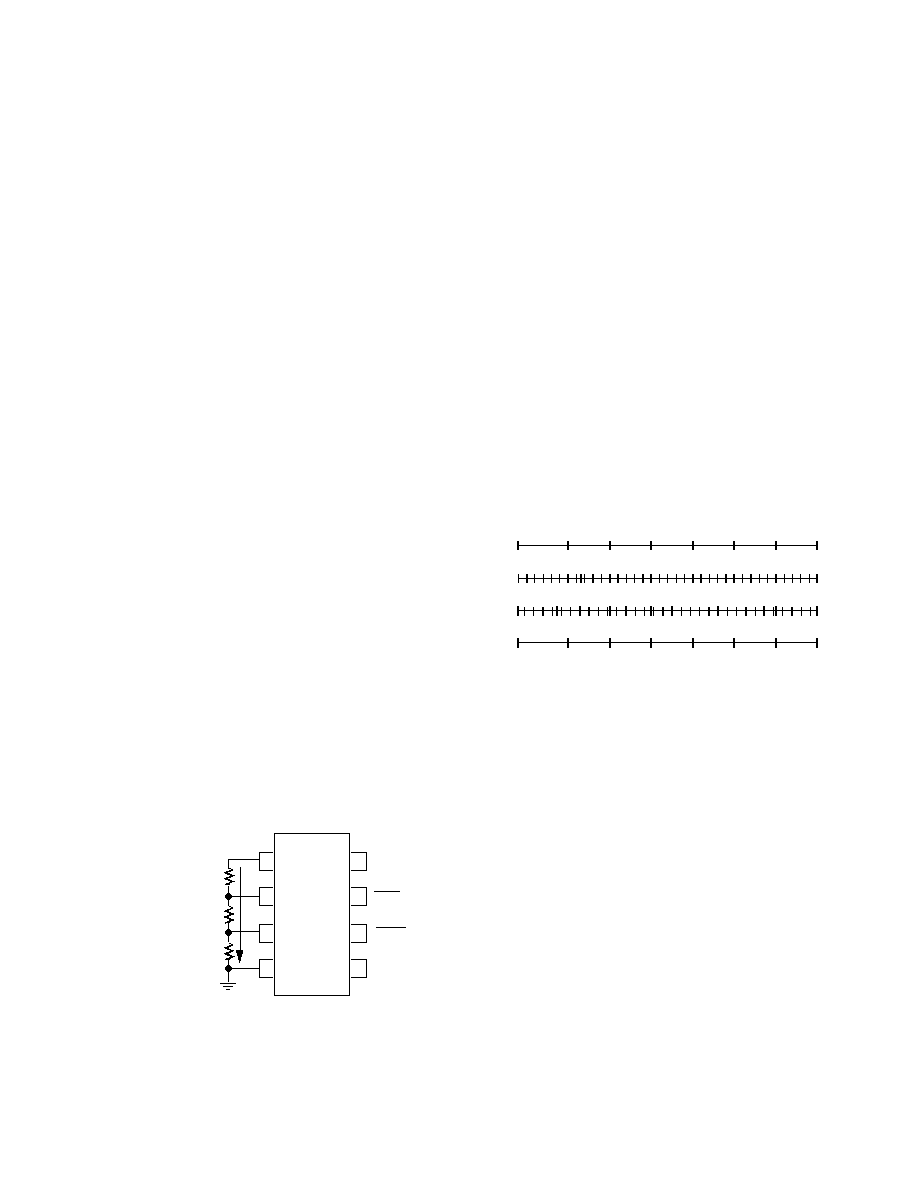
A simple method of measuring the TMP12 VPTAT is shown in
Figure 20. To measure VPTAT, adjust potentiometer R1 until
the LED turns ON. The voltage at Pin 2 of the TMP12 will
then match the TMP12's internal VPTAT.
VPTAT
TMP12
VREF
SET
HIGH
GND
V+
HEATER
1
2
3
4
5
6
7
8
200K
200K
+5V
NC
R1
+5V
R1
330
+5V
LED
OVER
UNDER
SET
LOW
Figure 20. Measuring VPTAT with a Potentiometer
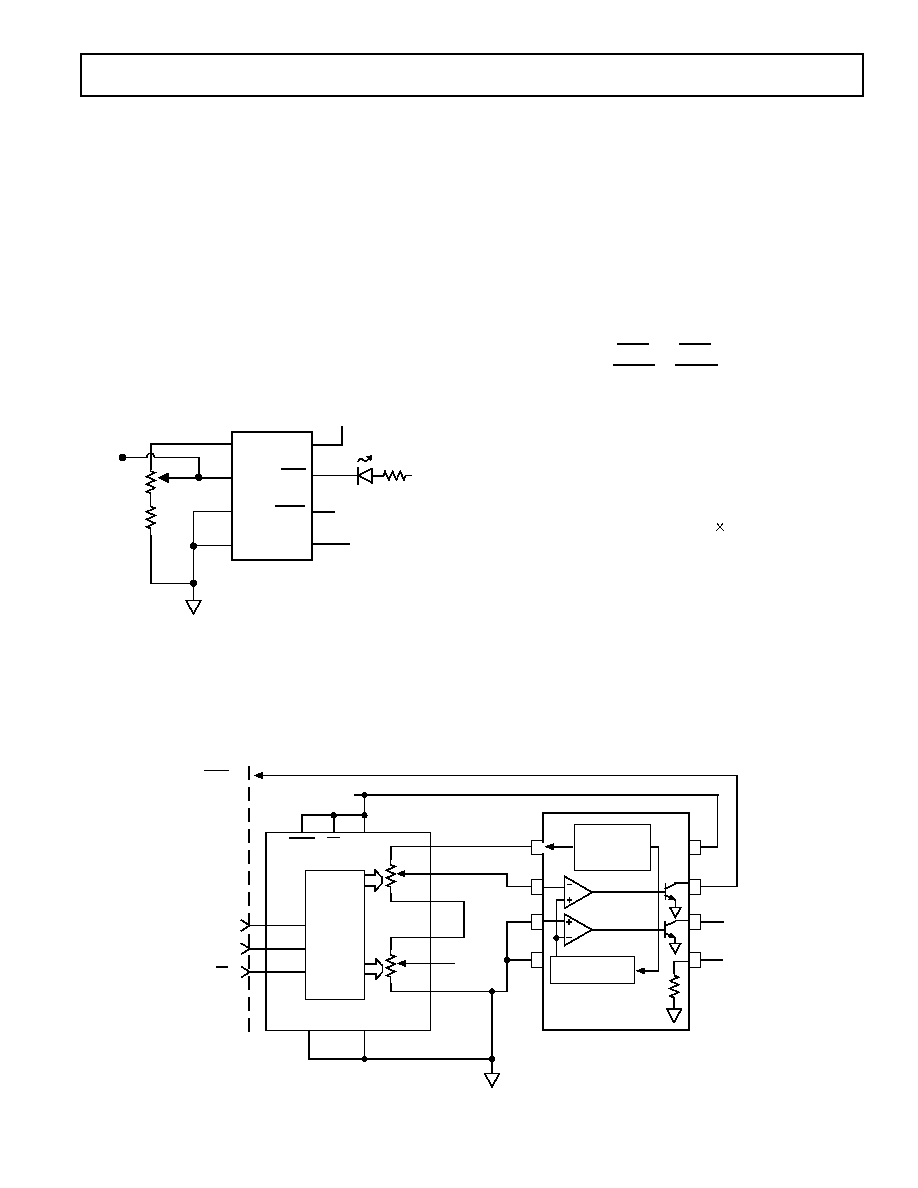
The method described in Figure 20 can be automated by replac-
ing the discrete resistors with a digital potentiometer. The
improved circuit, shown in Figure 21, permits the VPTAT volt-
age to be monitored with a microprocessor or other digital
controller. The AD8402-100 provides two 100 k
potentiom-
eters which are adjusted to 8-bit resolution via a 3-wire se-
rial interface. The controller simply sweeps the wiper of
potentiometer 1 from the A1 terminal to the B1 terminal
(digital value = 0), while monitoring the comparator output
at Pin 7 of the TMP12. When Pin 7 goes low, the voltage
at Pin 2 equals the VPTAT voltage. This Circuit sweeps
Pin 2's voltage from maximum to minimum, so that the
TMP12's setpoint hystersis will not affect the reading.
The circuit of Figure 21 provides approximately 1
°
C of
resolution. The two potentiometers divide VREF by two,
and the 8-bit potentiometer further divides VREF by 256,
so the resolution is:
Resolution =
= 4.9 mV
VREF
2
2N
2.5 V
2
28
=
where VREF is the voltage reference output (Pin 1 of the
TMP12) and N is the resolution of the AD8402. Since the
VPTAT has a slope of 5 mV/K, the AD8402 provides 1
°
C
of resolution. The adjustment range of this circuit extends
from VREF/2 (i.e. 1.25 V, or 23
°
C) to VREF 1 LSB
(i.e. 2.5 V 4.9 mV, or 226
°
C). The VPTAT is therefore:
VPTAT = 1.25 V + (Digital Count 4.9 mV)
where Digital Count is the value sent to the AD8402 which
caused the setpoint 1 output to go LOW.
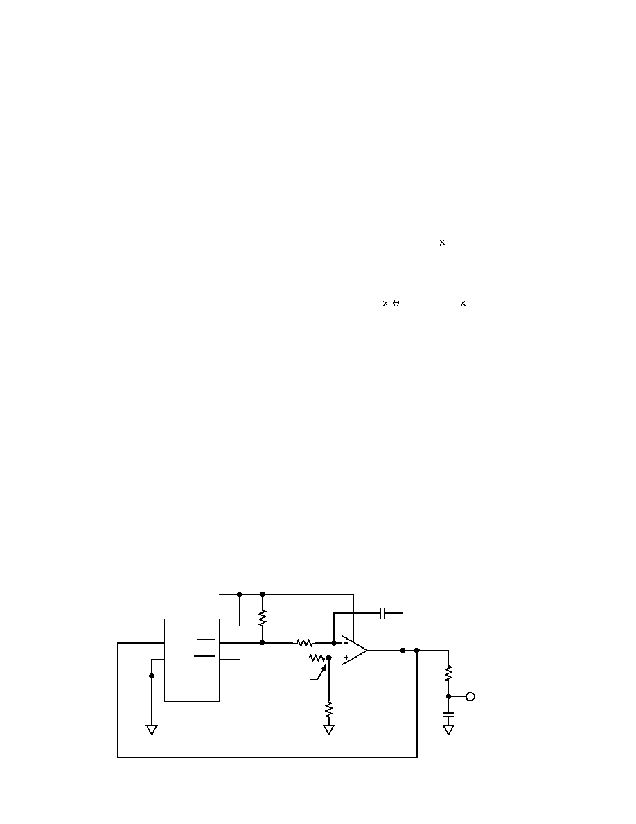
A third way to measure the VPTAT voltage is to close a
feedback loop around one of the TMP12's comparators.
This causes the comparator to oscillate, and in turn forces
the voltage at the comparator input to equal the VPTAT
voltage. Figure 22 is a typical circuit for this measurement.
An OP193 operational amplifier, operating as an integrator,
provides additional loop-gain to ensure that the TMP12
comparator will oscillate.
TEMPERATURE
SENSOR &
VOLTAGE
REFERENCE
1
2
3
4
HYSTERESIS
GENERATOR
WINDOW
COMPARATOR
VPTAT
VREF
7
8
5
6
TMP12
SERIAL
DATA
INTERFACE
1
5
6
7
8
9
10
11
B2
2
A2
3
W2
4
W1
12
A1
13
B1
14
100
DGND
AGND
SDI
CLK
CS
AD8402100
µC
INTERFACE
V
DD
RS
SHDN
OVER
+5V
+5V
NC
NC
Figure 21. Measuring VPTAT with a Digital Potentiometer
TMP12
REV. 0
10
Understanding Error Sources
The accuracy of the VPTAT sensor output is well characterized
and specified, however preserving this accuracy in a thermal
monitoring control system requires some attention to minimiz-
ing the various potential error sources. The internal sources of
setpoint programming error include the initial tolerances and
temperature drifts of the reference voltage VREF, the setpoint
comparator input offset voltage and bias current, and the hyster-
esis current scale factor. When evaluating setpoint programming
errors, remember that any VREF error contribution at the com-
parator inputs is reduced by the resistor divider ratios. Each
comparator's input bias current drops to less than 1 nA (typ)
when the comparator is tripped. This change accounts for some
setpoint voltage error, equal to the change in bias current multi-
plied by the effective setpoint divider ladder resistance to ground.
The thermal mass of the TMP12 package and the degree of
thermal coupling to the surrounding circuitry are the largest fac-
tors in determining the rate of thermal settling, which ultimately
determines the rate at which the desired temperature measure-
ment accuracy may be reached (see graph in Figure 3). Thus,
one must allow sufficient time for the device to reach the final
temperature. The typical thermal time constant for the SOIC
plastic package is approximately 70 seconds in still air. There-
fore, to reach the final temperature accuracy within 1%, for a
temperature change of 60 degrees, a settling time of 5 time con-
stants, or 6 minutes, is necessary. Refer to Figure 4.
External error sources to consider are the accuracy of the external
programming resistors, grounding error voltages, and thermal gra-
dients. The accuracy of the external programming resistors directly
impacts the resulting setpoint accuracy. Thus, in fixed-temperature
applications the user should select resistor tolerances appropriate
to the desired programming accuracy. Since setpoint resistors are
typically located in the same air flow as the TMP12, resistor tem-
perature drift must be taken into account also. This effect can be
minimized by selecting good quality components, and by keep-
ing all components in close thermal proximity. Careful circuit
board layout and component placement are necessary to mini-
mize common thermal error sources. Also, the user should take
care to keep the bottom of the setpoint programming divider
ladder as close to GND (Pin 4) as possible to minimize errors
due to IR voltage drops and coupling of external noise sources.
In any case, a 0.1
µ
F capacitor for power supply bypassing is
always recommended at the chip.
Safety Considerations in Heating and Cooling System Design
Designers should anticipate potential system fault conditions
that may result in significant safety hazards which are outside
the control of and cannot be corrected by the TMP12-based cir-
cuit. Governmental and Industrial regulations regarding safety
requirements and standards for such designs should be observed
where applicable.
Self-Heating Effects
In some applications the user should consider the effects of self-
heating due to the power dissipated by the open-collector outputs,
which are capable of sinking 20 mA continuously. Under full load,
the TMP12 open-collector output device is dissipating:
P
DISS
= 0.6 V
0.020 A = 12 mW
which in a surface-mount SO package accounts for a tempera-
ture increase due to self-heating of:
T
=
P
DISS
JA
=
0.012 W 158
°
C/W = 1.9
°
C
This increase is for still air, of course, and will be reduced at
high airflow levels. However, the user should still be aware that
self-heating effects can directly affect the accuracy of the
TMP12. For setpoint 2, self-heating will add to the setpoint
temperature (that is, in the above example the TMP12 will
switch the setpoint 2 output off 1.9 degrees early). Self-heating
will not affect the temperature at which setpoint 1 turns on, but
will add to the hysteresis. Several circuits for adding external
driver transistors and other buffers are presented in following
sections of this data sheet. These buffers will reduce self-heating
and improve accuracy.
Buffering the Voltage Reference
The reference output VREF is used to generate the temperature
setpoint programming voltages for the TMP12. Since the hyster-
esis is set by the reference current, external circuits which draw
current from the reference will increase the hysteresis value.
5
6
7
8
OP193
VREF
SET
HIGH
SET
LOW
GND
V+
HEATER
1
2
3
4
TMP12
130k
+5V
~1.5V
200k
5k
NC
NC
+5V
+5V
1uF
300k
10k
0.1UF
VPTAT
OVER
UNDER
Figure 22. An Analog Measurement Circuit for VPTAT
TMP12
REV. 0
11
The on-board VREF output buffer is typically capable of 500
µ
A
output drive into as much as 50 pF load (max). Exceeding this
load will affect the accuracy of the reference voltage, could cause
thermal sensing errors due to excess heat build-up, and may induce
oscillations. External buffering of VREF with a low-drift voltage
follower will ensure optimal reference accuracy. Amplifiers which
offer low drift, low power consumption, and low cost appropriate
to this application include the OP284, and members of the OP113
and OP193 families.
With excellent drift and noise characteristics, VREF offers a good
voltage reference for data acquisition and transducer excitation ap-
plications as well. Output drift is typically better than 10 ppm/
°
C,
with 315 nV/Hz (typ) noise spectral density at 1 kHz.
Preserving Accuracy Over Wide Temperature Range Operation
The TMP12 is unique in offering both a wide-range temperature
sensor and the associated detection circuitry needed to implement
a complete thermostatic control function in one monolithic device.
The voltage reference, setpoint comparators, and output buffer
amplifiers have been carefully compensated to maintain accuracy
over the specified temperature ranges in this application. Since the
TMP12 is both sensor and control circuit, in many applications the
external components used to program and interface the device are
subjected to the same temperature extremes. Thus, it is necessary
to place components in close thermal proximity minimizing large
temperate differentials, and to account for thermal drift errors
where appropriate, such as resistor matching temperature coeffi-
cients, amplifier error drift, and the like. Circuit design with the
TMP12 requires a slightly different perspective regarding the ther-
mal behavior of electronic components.
PC Board Layout Considerations
The TMP12 also requires a different perspective on PC board lay-
out. In many applications, wide traces and generous ground planes
are used to extract heat from components. The TMP12 is slightly
different, in that ideal path for heat is via the cooling system air
flow. Thus, heat paths through the PC traces should be minimized.
This constraint implies that minimum pad sizes and trace widths
should be specified in order to reduce heat conduction. At the
same time, analog performance should not be compromised. In
particular, the bottom of the setpoint resistor ladder should be
located as close to GND as possible, as discussed in the Under-
standing Error Sources section of this data sheet.
Thermal Response Time
The time required for a temperature sensor to settle to a
specified accuracy is a function of the thermal mass of the
sensor, and the thermal conductivity between the sensor and
the object being sensed. Thermal mass is often considered
equivalent to capacitance. Thermal conductivity is commonly
specified using the symbol Q, and is the inverse of thermal
resistance. It is commonly specified in units of degrees per
watt of power transferred across the thermal joint. Figures 3
and 5 illustrate the typical RC time constant response to a
step change in ambient temperature. Thus, the time required
for the TMP12 to settle to the desired accuracy is dependent
on the package selected, the thermal contact established in
the particular application, and the equivalent thermal con-
ductivity of the heat source. For most applications, the
settling-time is probably best determined empirically.
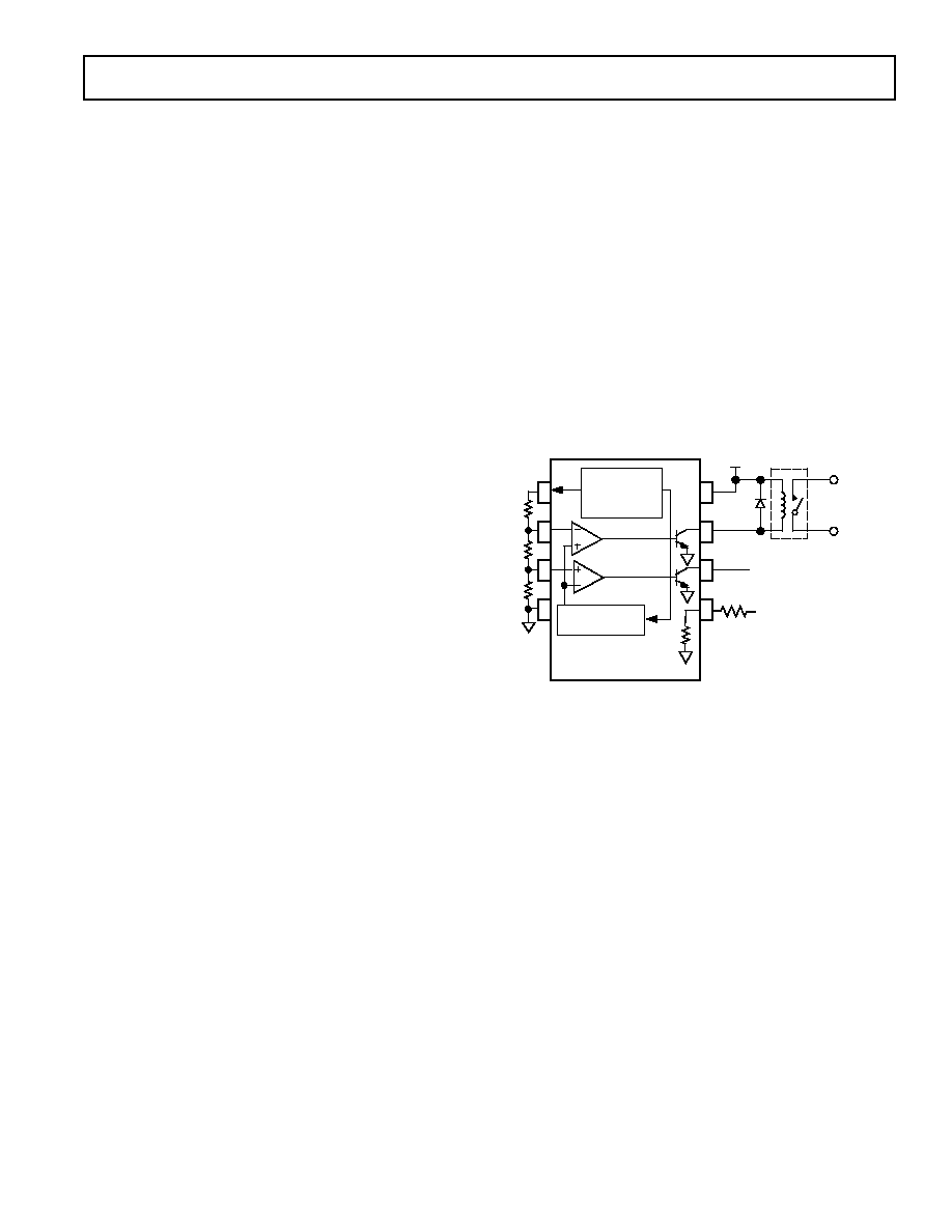
Switching Loads with the Open-Collector Outputs
In many temperature sensing and control applications some
type of switching is required. Whether it be to turn on a
heater when the temperature goes below a minimum value
or to turn off a motor that is overheating, the open-collector
outputs can be used. For the majority of applications, the
switches used need to handle large currents on the order of
1 Amp and above. Because the TMP12 is accurately mea-
suring temperature, the open-collector outputs should
handle less than 20 mA of current to minimize self-heating.
Clearly, the trip point outputs should not drive the equip-
ment directly. Instead, an external switching device is
required to handle the large currents. Some examples of
these are relays, power MOSFETs, thyristors, IGBTs, and
Darlington transistors.
This section shows a variety of circuits where the TMP12
controls a switch. The main consideration in these circuits,
such as the relay in Figure 23, is the current required to ac-
tivate the switch.
HYSTERESIS
GENERATOR
WINDOW
COMPARATOR
VPTAT
VREF
100
MOTOR
SHUTDOWN
2604-12-311
COTO
IN4001
OR EQUIV
+12V
R1
R2
R3
1
2
3
4
8
5
7
6
TMP12
NC
+12 V
140
TEMPERATURE
SENSOR &
VOLTAGE
REFERENCE
Figure 23. Reed Relay Drive
It is important to check the particular relay you choose to
ensure that the current needed to activate the coil does not
exceed the TMP12's recommended output current of
20 mA. This is easily determined by dividing the relay coil
voltage by the specified coil resistance. Keep in mind that
the inductance of the relay will create large voltage spikes
that can damage the TMP12 output unless protected by a
commutation diode across the coil, as shown. The relay
shown has contact rating of 10 Watts maximum. If a relay
capable of handling more power is desired, the larger con-
tacts will probably require a commensurably larger coil,
with lower coil resistance and thus higher trigger current.
As the contact power handling capability increases, so does
the current needed for the coil, In some cases an external
driving transistor should be used to remove the current load
on the TMP12 as explained in the next section.
TMP12
REV. 0
12
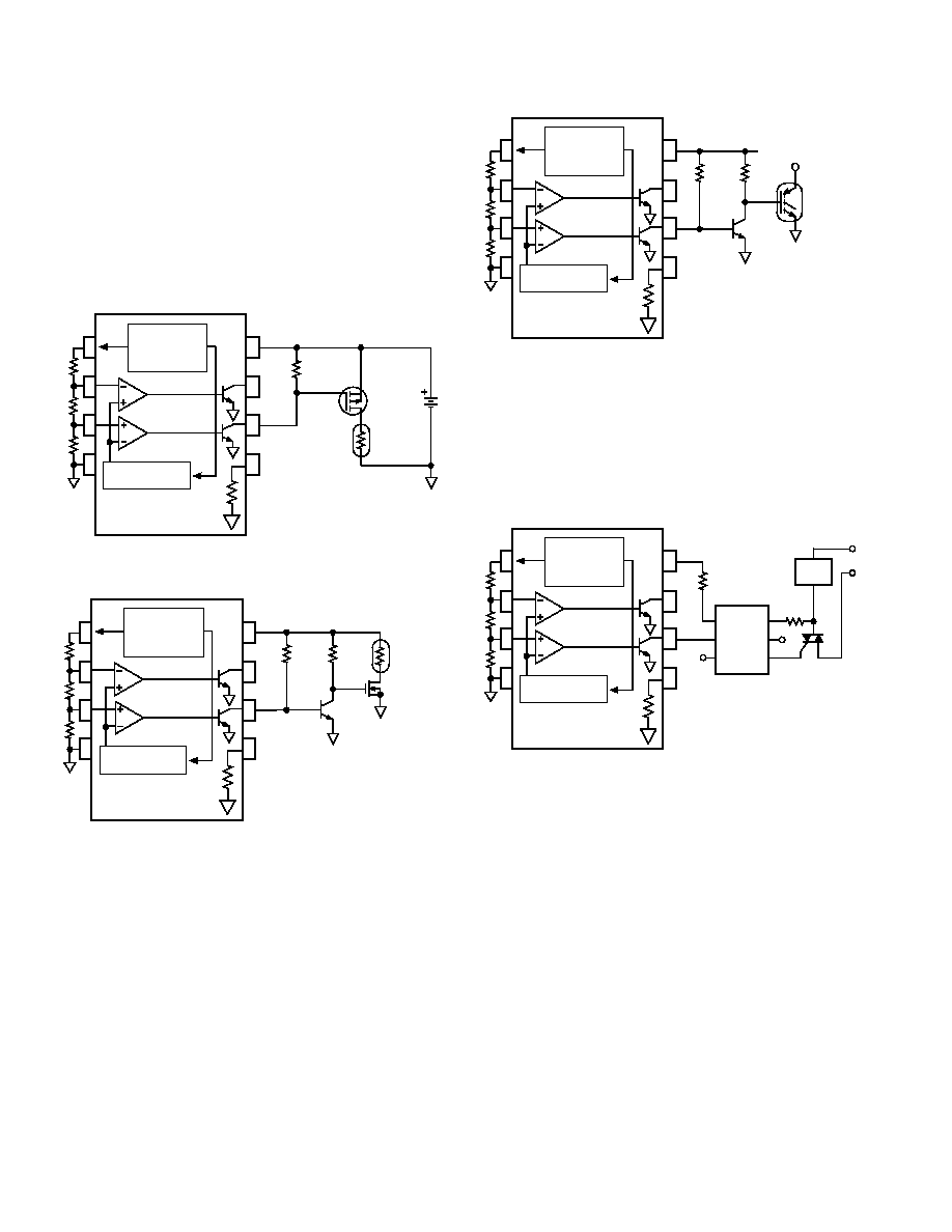
Power FETs are popular for handling a variety of high current
dc loads. Figure 24 shows the TMP12 driving a P-channel
MOSFET transistor for a simple heater circuit. When the out-
put transistor turns on, the gate of the MOSFET is pulled down
to approximately 0.6 V, turning it on. For most MOSFETs a
gate-to-source voltage or Vgs on the order of -2 V to -5 V is suf-
ficient to turn the device on. Figure 25 shows a similar circuit
for turning on an N-channel MOSFET, except that now the
gate to source voltage is positive. For this reason an external
transistor must be used as an inverter so that the MOSFET will
turn on when the trip point pulls down.
NC
IRFR9024
OR EQUIV
HEATING
ELEMENT
2.4k
(12V)
1.2k
(6V)
5%
V+
TEMPERATURE
SENSOR &
VOLTAGE
REFERENCE
HYSTERESIS
GENERATOR
WINDOW
COMPARATOR
VPTAT
VREF
100
1
2
3
4
8
5
7
6
+5V
TMP12
NC = NO CONNECT
Figure 24. Driving a P-Channel MOSFET
IRF130
NC
2N1711
HEATING
ELEMENT
V+
4.7k
4.7k
TEMPERATURE
SENSOR &
VOLTAGE
REFERENCE
HYSTERESIS
GENERATOR
WINDOW
COMPARATOR
VPTAT
VREF
100
1
2
3
4
8
5
7
6
+5V
TMP12
Figure 25. Driving an N-Channel MOSFET
Isolated Gate Bipolar Transistors (IGBTs) combine many of the
benefits of power MOSFETs with bipolar transistors and are
used for a variety of high power applications. Because IGBTs
have a gate similar to MOSFETs, turning on and off the devices
is relatively simple as shown in Figure 26. The turn on voltage
for the IGBT shown (IRGB40S) is between 3.0 and 5.5 volts.
This part has a continuous collector current rating of 50 A and a
maximum collector to emitter voltage of 600 V, enabling it to
work in very demanding applications.
IRGBC40S
NC
2N1711
V+
4.7k
4.7k
MOTOR
CONTROL
+5V
TEMPERATURE
SENSOR &
VOLTAGE
REFERENCE
HYSTERESIS
GENERATOR
WINDOW
COMPARATOR
VPTAT
VREF
100
1
2
3
4
8
5
7
6
TMP12
NC = NO CONNECT
Figure 26. Driving an IGBT
The last class of high power devices discussed here are Thyristors,
which include SCRs and Triacs. Triacs are a useful alternative to
relays for switching ac line voltages. The 2N6073A shown in Fig-
ure 27 is rated to handle 4 A (rms). The opto-isolated MOC3021
Triac shown features excellent electrical isolation from the noisy ac
line and complete control over the high power Triac with only a
few additional components.
NC
V+ = 5V
300
150
MOC3011
1
2
3
4
5
6
LOAD
AC
2N6073A
NC = NO CONNECT
TEMPERATURE
SENSOR &
VOLTAGE
REFERENCE
HYSTERESIS
GENERATOR
WINDOW
COMPARATOR
VPTAT
VREF
100
1
2
3
4
8
5
7
6
+5V
TMP12
Figure 27. Controlling the 2N6073A Triac
TMP12
REV. 0
13
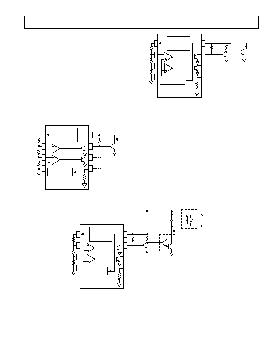
High Current Switching
As mentioned earlier, internal dissipation due to large loads on
the TMP12 outputs will cause some temperature error due to
self-heating. External transistors buffer the load from the
TMP12 so that virtually no power is dissipated in the internal
transistors and minimal self-heating occurs. This section shows
several examples using external transistors. The simplest case
uses a single transistor on the output to invert the output signal
is shown in Figure 28. When the open-collector of the TMP12
turns "ON" and pulls the output down, the external transistor
Q1's base will be pulled low, turning off the transistor. Another
transistor can be added to re-invert the signal as shown in Figure
29. Now, when the output of the TMP12 is pulled down, the
first transistor, Q1, turns off and its collector goes high, which
turns Q2 on, pulling its collector low. Thus, the output taken
from the collector of Q2 is identical to the output of the TMP12.
By picking a transistor that can accommodate large amounts of
current, many high power devices can be switched.
2N1711
V+
4.7k
I
C
Q1
TEMPERATURE
SENSOR &
VOLTAGE
REFERENCE
HYSTERESIS
GENERATOR
WINDOW
COMPARATOR
VPTAT
VREF
100
1
2
3
4
8
5
7
6
TMP12
Figure 28. An External Transistor Minimizes Self-Heating
MOTOR
SWITCH
RELAY
+12V
2N1711
V+
4.7k
I
C
4.7k
TIP-110
TEMPERATURE
SENSOR &
VOLTAGE
REFERENCE
HYSTERESIS
GENERATOR
WINDOW
COMPARATOR
VPTAT
VREF
100
1
2
3
4
8
5
7
6
+5V
TMP12
Figure 30. Darlington Transistor Can Handle Large Currents
Q1
Q2
2N1711
V+
4.7k
4.7k
2N1711
TEMPERATURE
SENSOR &
VOLTAGE
REFERENCE
HYSTERESIS
GENERATOR
WINDOW
COMPARATOR
VPTAT
VREF
100
1
2
3
4
8
5
7
6
TMP12
I
C
Figure 29. Second Transistor Maintains Polarity of TMP12
Output
An example of a higher power transistor is a standard
Darlington configuration as shown in Figure 30. The part cho-
sen, TIP-110, can handle 2 A continuous which is more than
enough to control many high power relays. In fact the
Darlington itself can be used as the switch, similar to
MOSFETs and IGBTs.
TMP12
REV. 0
14
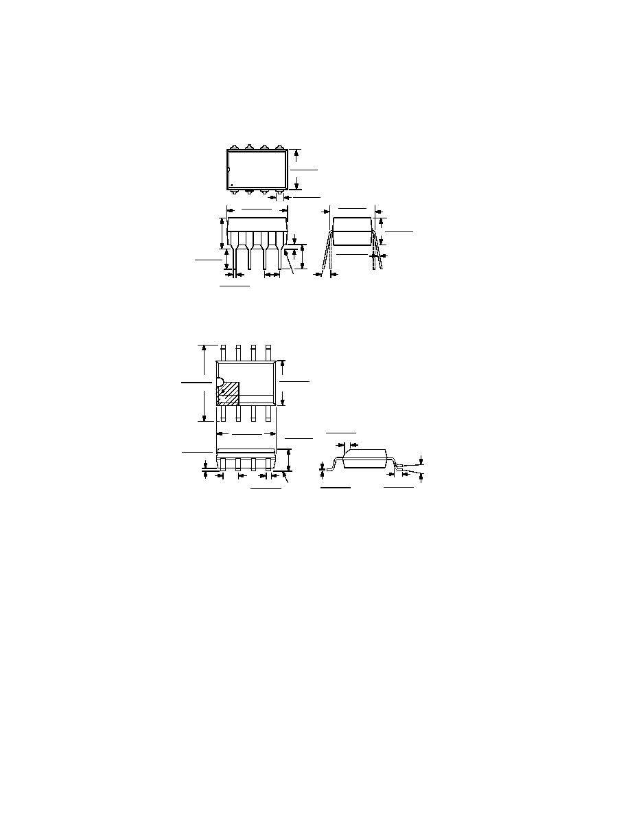
OUTLINE DIMENSIONS
Dimensions shown in inches and (mm).
8-Pin Epoxy DIP
0.015 (0.381)
0.008 (0.204)
0.160 (4.06)
0.115 (2.93)
0.130
(3.30)
MIN
0.210
(5.33)
MAX
0.015
(0.381) TYP
0.430 (10.92)
0.348 (8.84)
0.280 (7.11)
0.240 (6.10)
4
5
8
1
0.070 (1.77)
0.045 (1.15)
0.022 (0.558)
0.014 (0.356)
0.325 (8.25)
0.300 (7.62)
0°- 15°
0.100
(2.54)
BSC
SEATING
PLANE
0.195 (4.95)
0.115 (2.93)
8-Pin SOIC
SEATING
PLANE
0.0500 (1.27) BSC
4
5
8
1
0.2440 (6.20)
0.2284 (5.80)
0.1574 (4.00)
0.1497 (3.80)
0.1968 (5.00)
0.1890 (4.80)
0.0500 (1.27)
0.0160 (0.41)
0°-
8°
×
45°
0.0196 (0.50)
0.0099 (0.25)
0.0098 (0.25)
0.0075 (0.19)
0.0192 (0.49)
0.0138 (0.35)
0.0098 (0.25)
0.0040 (0.10)
0.102 (2.59)
0.094 (2.39)
C2074-10-10/95
PRINTED IN U.S.A.