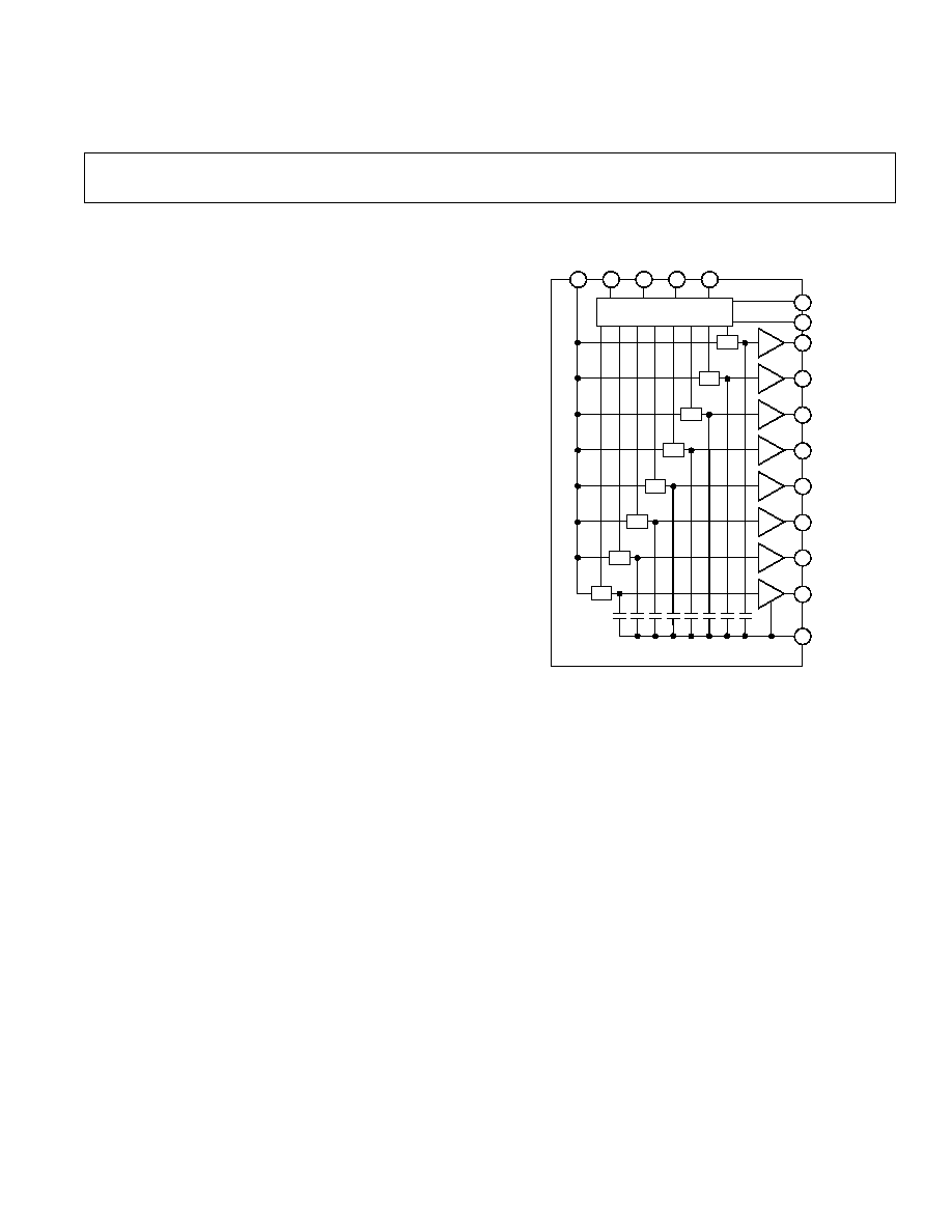
SMP08* Octal Sample-and-Hold with Mulitplexed Input
REV. D
Information furnished by Analog Devices is believed to be accurate and
reliable. However, no responsibility is assumed by Analog Devices for its
use, nor for any infringements of patents or other rights of third parties
which may result from its use. No license is granted by implication or
otherwise under any patent or patent rights of Analog Devices.
a
Octal Sample-and-Hold
with Multiplexed Input
SMP08*
FUNCTIONAL BLOCK DIAGRAM
SW
SW
SW
SW
SW
SW
SW
SW
1 OF 8 DECODER
6
9
10
11
3
13
16
8
14
15
12
7
1
2
4
5
DGND
V
DD
CH
0
OUT
CH
1
OUT
CH
2
OUT
CH
3
OUT
CH
4
OUT
CH
5
OUT
CH
6
OUT
CH
7
OUT
V
SS
HOLD CAPS
(INTERNAL)
SMP08
INPUT
(LSB)
A
B
(MSB)
C
INH
FEATURES
Internal Hold Capacitors
Low Droop Rate
TTL/CMOS Compatible Logic Inputs
Single or Dual Supply Operation
Break-Before-Make Channel Addressing
Compatible With CD4051 Pinout
Low Cost
APPLICATIONS
Multiple Path Timing Deskew for ATE
Memory Programmers
Mass Flow/Process Control Systems
Multichannel Data Acquisition Systems
Robotics and Control Systems
Medical and Analytical Instrumentation
Event Analysis
Stage Lighting Control
GENERAL DESCRIPTION
The SMP08 is a monolithic octal sample-and-hold; it has eight
internal buffer amplifiers, input multiplexer, and internal hold
capacitors. It is manufactured in an advanced oxide isolated
CMOS technology to obtain high accuracy, low droop rate, and
fast acquisition time. The SMP08 has a typical linearity error of
only 0.01% and can accurately acquire a 10-bit input signal to
±
1/2 LSB in less than 7 microseconds. The SMP08's output
swing includes the negative supply in both single and dual sup-
ply operation.
The SMP08 was specifically designed for systems that use a
calibration cycle to adjust a multiple of system parameters. The
low cost and high level of integration make the SMP08 ideal for
calibration requirements that have previously required an
ASIC, or high cost multiple D/A converters.
*Protected by U.S. Patent No. 4,739,281.
One Technology Way, P.O. Box 9106, Norwood, MA 02062-9106, U.S.A.
Tel: 617/329-4700
World Wide Web Site: http://www.analog.com
Fax: 617/326-8703
© Analog Devices, Inc., 1996
The SMP08 is also ideally suited for a wide variety of sample-
and-hold applications including amplifier offset or VCA gain
adjustments. One or more SMP08s can be used with single or
multiple DACs to provide multiple set points within a system.
The SMP08 offers significant cost and size reduction over dis-
crete designs. It is available in a 16-pin plastic DIP, or surface-
mount SOIC package.
2
SMP08SPECIFICATIONS
ELECTRICAL CHARACTERISTICS
Parameter
Symbol
Conditions
Min
Typ
Max
Units
Linearity Error
3 V
V
IN
+3 V
0.01
%
Buffer Offset Voltage
V
OS
T
A
= +25
°
C, V
IN
= 0 V
2.5
10
mV
40
°
C
T
A
+85
°
C, V
IN
= 0 V
3.5
20
mV
Hold Step
V
HS
V
IN
= 0 V, T
A
= +25
°
C to +85
°
C
2.5
4
mV
V
IN
= 0 V, T
A
= 40
°
C
5
mV
Droop Rate
V
CH
/
t
T
A
= +25
°
C, V
IN
= 0 V
2
20
mV/s
Output Source Current
I
SOURCE
V
IN
= 0 V
1
1.2
mA
Output Sink Current
I
SINK
V
IN
= 0 V
1
0.5
mA
Output Voltage Range
R
L
= 20 k
3.0
+3.0
V
LOGIC CHARACTERISTICS
Logic Input High Voltage
V
INH
2.4
V
Logic Input Low Voltage
V
INL
0.8
V
Logic Input Current
I
IN
V
IN
= 2.4 V
0.5
1
µ
A
DYNAMIC PERFORMANCE
2
Acquisition Time
3
t
AQ
T
A
= +25
°
C, 3 V to +3 V to 0.1%
3.6
7
µ
s
Hold Mode Settling Time
t
H
To
±
1 mV of Final Value
1
µ
s
Channel Select Time
t
CH
90
ns
Channel Deselect Time
t
DCS
45
ns
Inhibit Recovery Time
t
IR
90
ns
Slew Rate
SR
3
V/
µ
s
Capacitive Load Stability
<30% Overshoot
500
pF
Analog Crosstalk
3 V to +3 V Step
72
dB
SUPPLY CHARACTERISTICS
Power Supply Rejection Ratio
PSRR
V
S
=
±
5 V to
±
6 V
60
75
dB
Supply Current
I
DD
T
A
= +25
°
C
4
7.5
mA
40
°
C
T
A
+85
°
C
5
9.5
mA
ELECTRICAL CHARACTERISTICS
Parameter
Symbol
Conditions
Min
Typ
Max
Units
Linearity Error
60 mV
V
IN
10 V
0.01
%
Buffer Offset Voltage
V
OS
T
A
= +25
°
C, V
IN
= 6 V
2.5
10
mV
40
°
C
T
A
+85
°
C, V
IN
= 6 V
3.5
20
mV
Hold Step
V
HS
V
IN
= 6 V, T
A
= +25
°
C to +85
°
C
2.5
4
mV
V
IN
= 6 V, T
A
= 40
°
C
5
mV
Droop Rate
V
CH
/
t
T
A
= +25
°
C, V
IN
= 6 V
2
20
mV/s
Output Source Current
I
SOURCE
V
IN
= 6 V
1
1.2
mA
Output Sink Current
I
SINK
V
IN
= 6 V
1
0.5
mA
Output Voltage Range
R
L
= 20 k
0.06
10.0
V
R
L
= 10 k
0.06
9.5
V
LOGIC CHARACTERISTICS
Logic Input High Voltage
V
INH
2.4
V
Logic Input Low Voltage
V
INL
0.8
V
Logic Input Current
I
IN
V
IN
= 2.4 V
0.5
1
µ
A
DYNAMIC PERFORMANCE
2
Acquisition Time
3
t
AQ
T
A
= +25
°
C, 0 V to 10 V to 0.1%
3.5
4.25
µ
s
40
°
C
T
A
+85
°
C
3.75
6.00
µ
s
Hold Mode Settling Time
t
H
To
±
1 mV of Final Value
1
µ
s
Channel Select Time
t
CH
90
ns
Channel Deselect Time
t
DCS
45
ns
Inhibit Recovery Time
t
IR
90
ns
Slew Rate
SR
R
L
= 20 k
4
3
4
V/
µ
s
Capacitive Load Stability
<30% Overshoot
500
pF
Analog Crosstalk
0 V to 10 V Step
72
dB
SUPPLY CHARACTERISTICS
Power Supply Rejection Ratio
PSRR
10.8 V
V
DD
13.2 V
60
75
dB
Supply Current
I
DD
T
A
= +25
°
C
6.0
8.0
mA
40
°
C
T
A
+85
°
C
8.0
10.0
mA
NOTES
1
Outputs are capable of sinking and sourcing over 20 mA but offset is guaranteed at specified load levels.
2
All input control signals are specified with t
r
= t
f
= 5 ns (10% to 90% of +5 V) and timed from a voltage level of 1.6 V.
3
This parameter is guaranteed without test.
4
Slew rate is measured in the sample mode with 0 V to 10 V step from 20% to 80%.
Specifications subject to change without notice.
(@ V
DD
= +5 V, V
SS
= 5 V, DGND = 0 V, R
L
= No Load, T
A
= 40 C to +85 C for SMP08F,
unless otherwise noted)
(@ V
DD
= +12 V, V
SS
= 0 V, DGND = 0 V, R
L
= No Load, T
A
= 40 C to +85 C for SMP08F,
unless otherwise noted)
REV. D
SMP08
3
REV. D
ABSOLUTE MAXIMUM RATINGS
V
DD
to DGND . . . . . . . . . . . . . . . . . . . . . . . . . . . 0.3 V, 17 V
V
DD
to V
SS
. . . . . . . . . . . . . . . . . . . . . . . . . . . . . . 0.3 V, 17 V
V
LOGIC
to DGND . . . . . . . . . . . . . . . . . . . . . . . . 0.3 V, V
DD
V
IN
to DGND . . . . . . . . . . . . . . . . . . . . . . . . . . . . . . V
SS
, V
DD
V
OUT
to DGND . . . . . . . . . . . . . . . . . . . . . . . . . . . . . V
SS
, V
DD
Analog Output Current . . . . . . . . . . . . . . . . . . . . . . .
±
20 mA
(Not Short-Circuit Protected)
Operating Temperature Range
FP, FS . . . . . . . . . . . . . . . . . . . . . . . . . . . . 40
°
C to +85
°
C
Junction Temperature . . . . . . . . . . . . . . . . . . . . . . . . +150
°
C
Storage Temperature . . . . . . . . . . . . . . . . . . 65
°
C to +150
°
C
Lead Temperature (Soldering, 60 sec) . . . . . . . . . . . . +300
°
C
Package Type
JA
*
JC
Units
16-Pin Plastic DIP (P)
76
33
°
C/W
16-Pin SOIC (S)
92
27
°
C/W
*
JA
is specified for worst case mounting conditions, i.e.,
JA
is specified for device
in socket for plastic DIP package;
JA
is specified for device soldered to printed
circuit board for SO package.
ORDERING GUIDE
Temperature
Package
Package
Model
Range
Description
Option
SMP08FP
40
°
C to +85
°
C
Plastic DIP
N-16
SMP08FS
40
°
C to +85
°
C
SO-16
R-16A
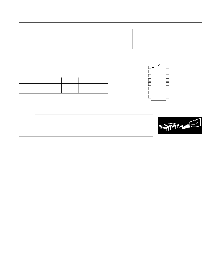
PIN CONNECTIONS
14
13
12
11
16
15
10
9
8
1
2
3
4
7
6
5
TOP VIEW
(Not to Scale)
SMP08
CH
4
OUT
CH
0
OUT
CH
1
OUT
CH
2
OUT
V
DD
CH
6
OUT
INPUT
CH
7
OUT
B CONTROL
A CONTROL
CH
3
OUT
CH
5
OUT
INH
V
SS
DGND
C CONTROL
WARNING!
ESD SENSITIVE DEVICE
CAUTION
ESD (electrostatic discharge) sensitive device. Electrostatic charges as high as 4000 V readily
accumulate on the human body and test equipment and can discharge without detection.
Although the SMP08 features proprietary ESD protection circuitry, permanent damage may
occur on devices subjected to high energy electrostatic discharges. Therefore, proper ESD
precautions are recommended to avoid performance degradation or loss of functionality.
4
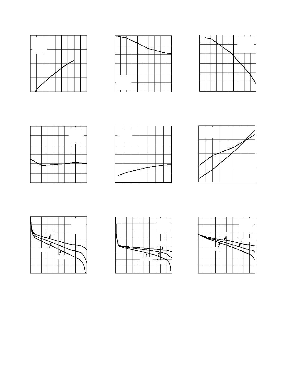
INPUT VOLTAGE Volts
DROOP RATE mV/s
1800
1200
600
0
1
10
2
3
4
5
6
7
8
9
1600
1400
1000
800
V
DD
= +12V
V
SS
= 0V
T
A
= +125
°
C
NO LOAD
Figure 3. Droop Rate vs. Input Voltage
V
DD
Volts
SLEW RATE V/µs
7
6
3
10
11
18
12
13
14
15
16
17
5
4
V
SS
= 0V
T
A
= +25
°
C
NO LOAD
SR
+SR
Figure 6. Slew Rate vs. V
DD
INPUT VOLTAGE Volts
OFFSET VOLTAGE mV
4
10
0
1
10
2
3
4
5
6
7
8
9
2
0
2
4
6
8
V
DD
= +12V
V
SS
= 0V
T
A
= 40
°
C
NO LOAD
R
L
=
R
L
= 20k
R
L
= 10k
Figure 9. Offset Voltage vs. Input
Voltage
INPUT VOLTAGE Volts
DROOP RATE mV/s
3
0
3
0
1
10
2
3
4
5
6
7
8
9
2
1
1
2
V
DD
= +12V
V
SS
= 0V
T
A
= +25
°
C
NO LOAD
Figure 2. Droop Rate vs. Input Voltage
TEMPERATURE
°
C
HOLD STEP mV
2
4
55
35
85
15
5
25
45
65
1
0
1
2
3
V
DD
= +12V
V
SS
= 0V
V
I N
= +5V
NO LOAD
Figure 5. Hold Step vs. Temperature
INPUT VOLTAGE Volts
OFFSET VOLTAGE mV
20
5
20
0
1
10
2
3
4
5
6
7
8
9
15
10
5
15
0
10
V
DD
= +12V
V
SS
= 0V
T
A
= +85
°
C
NO LOAD
R
L
=
R
L
= 20k
R
L
= 10k
Figure 8. Offset Voltage vs. Input
Voltage
REV. D
SMP08Typical Performance Characteristics
TEMPERATURE
°
C
DROOP RATE mV/s
1000
100
0.1
55 35
125
15
5
25
65
85
105
45
10
1
V
DD
= +12V
V
SS
= 0V
V
I N
= +5V
R
L
= 10k
Figure 1. Droop Rate vs. Temperature
INPUT VOLTAGE Volts
HOLD STEP mV
2
1
4
0
1
10
2
3
4
5
6
7
8
9
1
0
2
3
V
DD
= +12V
V
SS
= 0V
T
A
= +25
°
C
NO LOAD
Figure 4. Hold Step vs. Input Voltage
INPUT VOLTAGE Volts
OFFSET VOLTAGE mV
4
10
0
1
10
2
3
4
5
6
7
8
9
2
0
2
4
6
8
V
DD
= +12V
V
SS
= 0V
T
A
= +25
°
C
NO LOAD
R
L
=
R
L
= 20k
R
L
= 10k
Figure 7. Offset Voltage vs. Input
Voltage
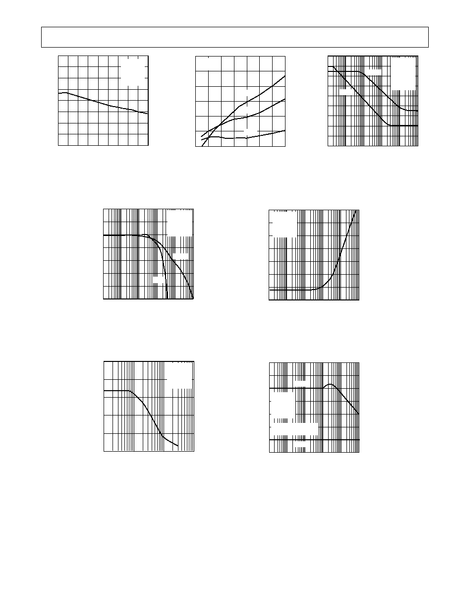
TEMPERATURE
°
C
OFFSET VOLTAGE mV
0
8
55 35
125
15
5
25
65
85
105
45
1
4
5
6
7
2
3
V
DD
= +12V
V
SS
= 0V
V
I N
= +5V
R
L
= 10k
Figure 10. Offset Voltage vs.
Temperature
V
DD
Volts
SUPPLY CURRENT mA
14
2
4
6
18
8
10
12
14
16
12
10
8
6
4
V
SS
= 0V
NO LOAD
+85
°
C
+25
°
C
40
°
C
Figure 11. Supply Current vs. V
DD
FREQUENCY Hz
90
80
0
10
100
1M
1k
10k
100k
70
60
20
50
40
30
10
REJECTION RATIO dB
V
DD
= +12V
V
SS
= 0V
V
I N
= +6V
T
A
= +25
°
C
NO LOAD
+PSRR
PSRR
Figure 12. Sample Mode Power
Supply Rejection
Typical Performance CharacteristicsSMP08
REV. D
5
FREQUENCY Hz
GAIN dB
2
1
5
100
1k
10M
10k
100k
1M
0
1
2
3
4
90
45
225
0
45
90
135
180
PHASE SHIFT Degrees
V
DD
= +12V
V
SS
= 0V
T
A
= +25
°
C
NO LOAD
GAIN
PHASE
Figure 13. Gain, Phase Shift vs.
Frequency
FREQUENCY Hz
PEAK-TO-PEAK OUTPUT Volts
15
12
0
10k
100k
10M
1M
9
6
3
V
DD
= +6V
V
SS
= 6V
T
A
= +25
°
C
NO LOAD
Figure 15. Maximum Output Voltage
vs. Frequency
FREQUENCY Hz
OUTPUT IMPEDANCE
35
30
0
10
100
1M
1k
10k
100k
25
20
15
10
5
V
DD
= +12V
V
SS
= 0V
T
A
= +25
°
C
NO LOAD
Figure 14. Output Impedance vs.
Frequency
FREQUENCY Hz
REJECTION RATIO dB
60
50
10
10
100
1M
1k
10k
100k
40
30
20
10
0
V
DD
= +12V
V
SS
= 0V
T
A
= +25
°
C
NO LOAD
+PSRR
HOLD CAPACITORS
REFERENCED TO V
SS
PSRR
Figure 16. Hold Mode Power Supply
Rejection
SMP08
6
REV. D
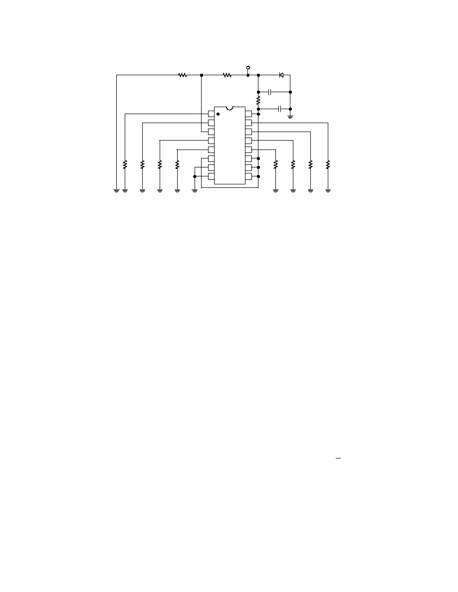
14
13
12
11
16
15
10
9
8
1
2
3
4
7
6
5
SMP08
R2
10k
R2
10k
R2
10k
R2
10k
R3
6.5k
R4
1k
R1
10
D1
C1
10µF
C2
1µF
+
V
CC
+15V
R2
10k
R2
10k
R2
10k
R2
10k
Figure 17. Burn-In Circuit
OUTPUT BUFFERS (Pins 1, 2, 4, 5, 12, 13, 14, 15)
The buffer offset specification is 10 mV; this is less than 1/2 LSB
of an 8-bit DAC with 10 V full scale. The hold step (magni-
tude of step caused in the output voltage when switching from
sample-to-hold mode, also referred to as the pedestal error or
sample-to-hold offset), is about 2.5 mV with little variation
over the full output voltage range, T
A
= +25
°
C to +85
°
C. The
droop rate of a held channel is 2 mV/s typical and 20 mV/s
maximum.
The buffers are designed to drive loads connected to ground.
The outputs can source more than 20 mA, over the full voltage
range, but have limited current sinking capability near V
SS
. In
split supply operation, symmetrical output swings can be ob-
tained by restricting the output range to 2 V from either supply.
On-chip SMP08 buffers eliminate potential stability problems
associated with external buffers; outputs are stable with ca-
pacitive loads up to 500 pF. However, since the SMP08's
buffer outputs are not short-circuit protected, care should be
taken to avoid shorting any output to the supplies or ground.
SIGNAL INPUT (Pin 3)
The signal input should be driven from a low impedance volt-
age source such as the output of an op amp. The op amp
should have a high slew rate and fast settling time if the
SMP08's acquisition time characteristics are to be maintained.
As with all CMOS devices, all input voltages should be kept
within range of the supply rails (V
SS
< V
IN
< V
DD
) to avoid the
possibility of latchup. If single supply operation is desired, op
amps such as the OP183 or AD820 that have input and output
voltage compliances including ground, can be used to drive the
inputs. Split supplies, such as
±
7.5 V, can be used with the
SMP08.
APPLICATION TIPS
All unused digital inputs should be connected to logic LOW
and unused analog inputs connected to analog ground. For
connector-driven analog inputs that may become temporarily
disconnected, a resistor to V
DD
, V
SS
or analog ground should
be used with a value ranging from 200 k
to 1 M
.
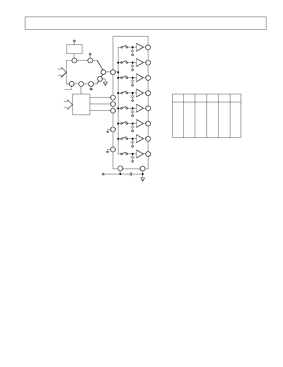
APPLICATIONS INFORMATION
The SMP08, a multiplexed octal S/H, minimizes board space in
systems requiring cycled calibration or an array of control volt-
ages. When used in conjunction with a low cost 16-bit D/A, the
SMP08 can easily be integrated into microprocessor based sys-
tems. Since the SMP08 features break-before-make switching
and an internal decoder, no external logic is required. The
SMP08 has an internally regulated TTL supply so that TTL/
CMOS compatibility is maintained over the full supply range.
See Figure 18 for channel decode address information.
POWER SUPPLIES
The SMP08 is capable of operating with either single or dual
supplies, over a voltage range of 7 volts to 15 volts. Based on the
supply voltages chosen, V
DD
and V
SS
establish the input and
output voltage range, which is:
(V
SS
+0.06 V)
V
OUT/IN
(V
DD
2 V)
Note that several specifications, including acquisition time, off-
set and output voltage compliance, will degrade for supply volt-
ages of less than 7 V.
If split supplies are used, the negative supply should be bypassed
with a 0.1
µ
F capacitor in parallel with a 10
µ
F to ground. The
internal hold capacitors are connected to this supply pin and any
noise will appear at the outputs.
In single supply applications, it is extremely important that the
V
SS
(negative supply) pin is connected to a clean ground. The
hold capacitors are internally tied to the V
SS
(negative) rail. Any
ground noise or disturbance will directly couple to the output of
the sample-and-hold, degrading the signal-to-noise perfor-
mance. The analog and digital ground traces on the circuit
board should be physically separated to reduce digital switching
noise from entering the analog circuitry.
POWER SUPPLY SEQUENCING
V
DD
should be applied to the SMP08 before the logic input sig-
nals. The SMP08 has been designed to be immune to latchup,
but standard precautions should still be taken.
SMP08
7
REV. D
V
SS
V
SS
V
SS
V
SS
V
SS
V
SS
V
SS
V
SS
SMP08
13
14
15
12
1
2
4
5
3
16
6
7
8
9
10
11
+12V
CH
0
CH
1
CH
2
CH
3
CH
4
CH
5
CH
6
CH
7
3
15
1
5
16
17
4
+12V
+5V
REF02
+12V
V
REF
A
V
DD
V
OA
V
Z
GND
WR
CS
DAC8228
A
B
C
ADDRESS
DECODE
ADDRESS
BUS
DIGITAL
INPUTS
WR
DGND
INH
0.1µF
PIN 9
C
PIN 10
B
PIN 11
A
PIN 6
INH
CH
PIN
0
0
0
0
1
1
1
1
X
0
0
1
1
0
0
1
1
X
0
1
0
1
0
1
0
1
X
0
0
0
0
0
0
0
0
1
0
1
2
3
4
5
6
7
NONE
13
14
15
12
1
5
2
4
CHANNEL DECODING
Figure 18. 8-Channel Multiplexed D/A Converter
Do not apply signals to the SMP08 with power off unless the
input current is limited to less than 10 mA.
TYPICAL APPLICATIONS
AN 8-CHANNEL MULTIPLEXED D/A CONVERTER
Figure 18 illustrates a typical demultiplexing function of the
SMP08. It is used to sample-and-hold eight different output
voltages corresponding to eight different digital codes from a
D/A converter. The SMP08's droop rate of 20 mV/s requires a
refresh once every 500 ms, before the voltage drifts beyond
1/2 LSB accuracy (1 LSB of an 8-bit DAC is equivalent to
19.5 mV out of a full-scale voltage of 5 V). For a 10-bit DAC
the refresh rate must be less than 120 ms, and, for a 12-bit
system, 31 ms. This implementation is very cost effective com-
pared to using multiple DACs as the number of output channels
increases.
SMP08
8
REV. D
C2192210/96
PRINTED IN U.S.A.
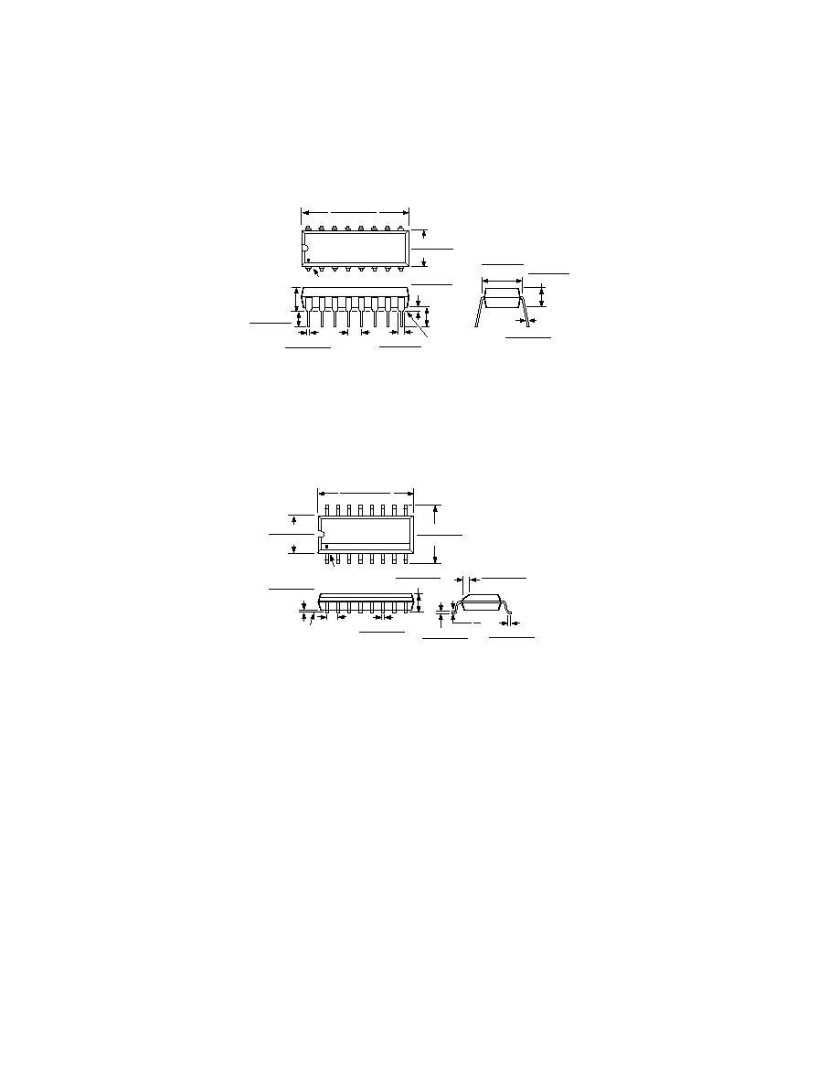
OUTLINE DIMENSIONS
Dimensions shown in inches and (mm).
16-Lead Plastic DIP
(N-16)
16
1
8
9
0.840 (21.33)
0.745 (18.93)
0.280 (7.11)
0.240 (6.10)
PIN 1
SEATING
PLANE
0.022 (0.558)
0.014 (0.356)
0.060 (1.52)
0.015 (0.38)
0.210 (5.33)
MAX
0.130
(3.30)
MIN
0.070 (1.77)
0.045 (1.15)
0.100
(2.54)
BSC
0.160 (4.06)
0.115 (2.93)
0.325 (8.25)
0.300 (7.62)
0.015 (0.381)
0.008 (0.204)
0.195 (4.95)
0.115 (2.93)
16-Lead SOIC (Narrow Body)
(SO-16)
16
9
8
1
0.3937 (10.00)
0.3859 (9.80)
0.2550 (6.20)
0.2284 (5.80)
0.1574 (4.00)
0.1497 (5.80)
PIN 1
SEATING
PLANE
0.0098 (0.25)
0.0040 (0.10)
0.0192 (0.49)
0.0138 (0.35)
0.0688 (1.75)
0.0532 (1.35)
0.0500
(1.27)
BSC
0.0099 (0.25)
0.0075 (0.19)
0.0500 (1.27)
0.0160 (0.41)
8
°
0
°
0.0196 (0.50)
0.0099 (0.25)
x 45
°