OP490 Low Voltage Micropower Quad Operational Amplifier
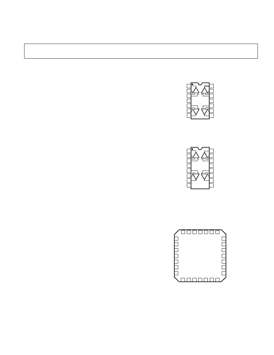
PIN CONNECTION
14-Pin Hermetic DIP (Y-Suffix)
14-Pin Plastic DIP (P-Suffix)
1
2
3
4
5
6
7
14
13
12
11
10
9
8
OUT A
IN A
+IN A
V+
+IN B
IN B
OUT B
IN D
+IN D
V
+IN C
IN C
OUT C
OUT D
16-Pin SOL (S-Suffix)
1
2
3
4
5
6
7
8
14
13
12
11
10
9
15
16
OUT A
IN A
+IN A
V+
+IN B
IN B
OUT B
IN D
+IN D
V
+IN C
IN C
OUT C
OUT D
NC
NC
NC = NO CONNECT
28-Pin LCC (TC-Suffix)
1
2
3
4
5
6
7
8
9
10
11
12
13
14
15
16
17
18
19
20
21
22
23
24
25
26
27
28
NC
+IN A
NC
V+
NC
+IN B
NC
NC
+IN D
NC
V
NC
+IN C
NC
NC
IN A
OUT A
NC
OUT D
IN D
NC
NC
IN B
OUT B
OUT C
IN C
NC
NC
NC = NO CONNECT
REV. B
Information furnished by Analog Devices is believed to be accurate and
reliable. However, no responsibility is assumed by Analog Devices for its
use, nor for any infringements of patents or other rights of third parties
which may result from its use. No license is granted by implication or
otherwise under any patent or patent rights of Analog Devices.
a
Low Voltage Micropower
Quad Operational Amplifier
OP490
One Technology Way, P.O. Box 9106, Norwood, MA 02062-9106, U.S.A.
Tel: 617/329-4700
Fax: 617/326-8703
FEATURES
Single/Dual Supply Operation
+1.6 V to +36 V
0.8 V to 18 V
True Single-Supply Operation; Input and Output
Voltage Ranges Include Ground
Low Supply Current: 80 A max
High Output Drive: 5 mA min
Low Offset Voltage: 0.5 mA max
High Open-Loop Gain: 700 V/mV min
Outstanding PSRR: 5.6 V/V min
Industry Standard Quad Pinouts
Available in Die Form
GENERAL DESCRIPTION
The OP490 is a high-performance micropower quad op amp
that operates from a single supply of +1.6 V to +36 V or from
dual supplies of
±
0.8 V to
±
18 V. Input voltage range includes
the negative rail allowing the OP490 to accommodate input sig-
nals down to ground in single-supply operation. The OP490's
output swing also includes ground when operating from a single
supply, enabling "zero-in, zero-out" operation.
The quad OP490 draws less than 20
µ
A of quiescent supply
current per amplifier, but each amplifier is able to deliver over
5 mA of output current to a load. Input offset voltage is under
0.5 mV with offset drift below 5
µ
V/
°
C over the military tem-
perature range. Gain exceeds over 700,000 and CMR is better
than 100 dB. A PSRR of under 5.6
µ
V/V minimizes offset volt-
age changes experienced in battery powered systems.
The quad OP490 combines high performance with the space
and cost savings of quad amplifiers. The minimal voltage and
current requirements of the OP490 makes it ideal for battery
and solar powered applications, such as portable instruments
and remote sensors.

REV. B
2
(@ V
S
= 1.5 V to 15 V, T
A
= +25 C, unless otherwise noted)
OP490SPECIFICATIONS
ELECTRICAL CHARACTERISTICS
OP490A/E
OP490F
OP490G
Parameter
Symbol
Conditions
Min
Typ
Max
Min
Typ
Max
Min
Typ Max Units
INPUT OFFSET VOLTAGE
V
OS
0.2
0.5
0.4
0.75
0.6
1.0
mV
INPUT OFFSET CURRENT
I
OS
V
CM
= 0 V
0.4
3
0.4
5
0.4
5
nA
INPUT BIAS CURRENT
I
B
V
CM
= 0 V
4.2
15
4.2
20
4.2
25
nA
LARGE SIGNAL VOLTAGE
A
VO
V
S
=
±
15 V, V
O
=
±
10 V
GAIN
R
L
= 100 k
700
1200
500
1000
400
800
V/mV
R
L
= 10 k
350
600
250
500
200
400
R
L
= 2 k
125
250
100
200
100
200
V+ = 5 V, V = 0 V,
1 V < V
O
< 4 V
R
L
= 100 k
200
400
125
300
100
250
R
L
= 10 k
100
180
75
140
70
140
INPUT VOLTAGE RANGE
IVR
V+ = 5 V, V = 0 V
0/4
0/4
0/4
V
V
S
=
±
15 V
1
15/13.5
15/13.5
15/13.5
OUTPUT VOLTAGE SWING
V
O
V
S
=
±
15 V
R
L
= 10 k
±
13.5
±
14.2
±
13.5
±
14.2
±
13.5
±
14.2
V
R
L
= 2 k
±
10.5
±
11.5
±
10.5
±
11.5
±
10.5
±
11.5
V
OH
V+ = 5 V, V = 0 V
R
L
= 2 k
4.0
4.2
4.0
4.2
4.0
4.2
V
V
OL
V+ = 5 V, V = 0 V
R
L
= 10 k
100
500
100
500
100
500
µ
V
COMMON-MODE
CMR
V+ = 5 V, V = 0 V,
90
110
80
100
80
100
dB
REJECTION
0 V < V
CM
< 4 V
V
S
=
±
15 V,
100
130
90
120
90
120
15 V < V
CM
< 13.5 V
POWER SUPPLY
REJECTION RATIO
PSRR
1.0
5.6
3.2
10
3.2
10
µ
V/V
SLEW RATE
SR
V
S
=
±
15 V
5
12
5
12
5
12
V/ms
SUPPLY CURRENT
V
S
=
±
1.5 V, No Load
40
60
40
60
40
60
µ
A
(ALL AMPLIFIERS)
I
SY
V
S
=
±
15 V, No Load
60
80
60
80
60
80
CAPACITIVE LOAD STABILITY
A
V
= +1
650
650
650
pF
INPUT NOISE VOLTAGE
e
n
p-p
f
O
= 0.1 Hz to 10 Hz
3
3
3
µ
V p-p
V
S
=
±
15 V
INPUT RESISTANCE
DIFFERENTIAL MODE
R
IN
V
S
=
±
15 V
30
30
30
M
INPUT RESISTANCE
COMMON MODE
R
INCM
V
S
=
±
15 V
20
20
20
G
GAIN BANDWIDTH PRODUCT
GBWP
A
V
= +1
20
20
20
kHz
CHANNEL SEPARATION
CS
f
O
= 10 Hz
120
150
120
150
120
150
dB
V
O
= 20 V p-p
V
S
=
±
15 V
2
NOTES
1
Guaranteed by CMR test.
2
Guaranteed but not 100% tested.
Specifications subject to change without notice.

OP490
REV. B
3
ELECTRICAL CHARACTERISTICS
OP490A
Parameter
Symbol
Conditions
Min
Typ
Max
Units
INPUT OFFSET VOLTAGE
V
OS
0.4
1.0
mV
AVERAGE INPUT OFFSET
VOLTAGE DRIFT
TCV
OS
V
S
=
±
15 V
2
5
µ
V/
°
C
INPUT OFFSET CURRENT
I
OS
V
CM
= 0 V
1.5
5
nA
INPUT BIAS CURRENT
I
B
V
CM
= 0 V
4.4
20
nA
LARGE-SIGNAL VOLTAGE GAIN
A
VO
V
S
=
±
15 V, V
O
=
±
10 V
R
L
= 100 k
225
400
V/mV
R
L
= 10 k
125
240
R
L
= 2 k
50
110
V+ = 5 V, V = 0 V,
1 V < V
O
< 4 V
R
L
= 100 k
100
200
R
L
= 10 k
50
110
INPUT VOLTAGE RANGE
IVR
V+ = 5 V, V = 0 V
0/3.5
V
V
S
=
±
15 V
1
15/13.5
OUTPUT VOLTAGE SWING
V
O
V
S
=
±
15 V
R
L
= 10 k
±
13
±
13.7
V
R
L
= 2 k
±
10
±
11
V
OH
V+ = 5 V, V = 0 V
R
L
= 2 k
3.9
4.1
V
V
OL
V+ = 5 V, V = 0 V
R
L
= 10 k
100
500
µ
V
COMMON-MODE REJECTION
CMR
V+ = 5 V, V = 0 V, 0 V < V
CM
< 3.5 V
85
105
dB
V
S
=
±
15 V, 15 V < V
CM
< 13.5 V
95
115
POWER SUPPLY REJECTION RATIO
PSRR
3.2
10
µ
V/V
SUPPLY CURRENT (ALL AMPLIFIERS)
I
SY
V
S
=
±
1.5 V, No Load
70
100
µ
A
V
S
=
±
15 V, No Load
90
120
NOTES
1
Guaranteed by CMR test.
Specifications subject to change without notice.
(@ V
S
= 1.5 V to 15 V, 55 C
T
A
+125 C, unless otherwise noted)
REV. B
4
OP490SPECIFICATIONS
ELECTRICAL CHARACTERISTICS
OP490E
OP490F
OP490G
Parameter
Symbol
Conditions
Min
Typ
Max
Min
Typ
Max
Min
Typ Max
Units
INPUT OFFSET VOLTAGE
V
OS
0.32
0.8
0.6
1.35
0.8
1.5
mV
AVERAGE INPUT OFFSET
VOLTAGE DRIVE
TCV
OS
V
S
=
±
15 V
2
5
4
4
µ
V/
°
C
INPUT OFFSET CURRENT
I
OS
V
CM
= 0 V
0.8
3
1.0
5
1.3
7
nA
INPUT BIAS CURRENT
I
B
V
CM
= 0 V
4.4
15
4.4
20
4.4
25
nA
LARGE SIGNAL VOLTAGE GAIN
A
VO
V
S
=
±
15 V, V
O
=
±
10 V
R
L
= 100 k
500
800
350
700
300
600
V/mV
R
L
= 10 k
250
400
175
250
150
250
R
L
= 2 k
100
200
75
150
75
125
V+ = 5 V, V = 0 V,
1 V < V
O
< 4 V
R
L
= 100 k
150
280
100
220
80
160
R
L
= 10 k
75
140
50
110
40
90
INPUT VOLTAGE RANGE
IVR
V+ = 5 V, V = 0 V
0/3.5
0/3.5
0/3.5
V
V
S
=
±
15 V
1
15/13.5
15/13.5
15/13.5
OUTPUT VOLTAGE SWING
V
O
V
S
=
±
15 V
R
L
= 10 k
±
13
±
14
±
13
±
14
±
13
±
14
V
R
L
= 2 k
±
10
±
11
±
10
±
11
±
10
±
11
V
OH
V+ = 5 V, V = 0 V
R
L
= 2 k
3.9
4.1
3.9
4.1
3.9
4.1
V
OL
V+ = 5 V, V = 0 V
R
L
= 10 k
100
500
100
500
100
500
µ
V
COMMON-MODE
CMR
V+ = 5 V, V = 0 V,
90
110
80
100
80
100
dB
REJECTION
0 V < V
CM
< 3.5 V
V
S
=
±
15 V,
100
120
90
110
90
110
15 V < V
CM
< 13.5 V
POWER SUPPLY
REJECTION RATIO
PSRR
1.0
5.6
3.2
10
5.6
17.8
µ
V/V
SUPPLY CURRENT
V
S
=
±
1.5 V, No Load
65
100
65
100
60
100
µ
A
(ALL AMPLIFIERS)
I
SY
V
S
=
±
15 V, No Load
80
120
80
120
75
120
NOTES
1
Guaranteed by CMR test.
Specifications subject to change without notice.
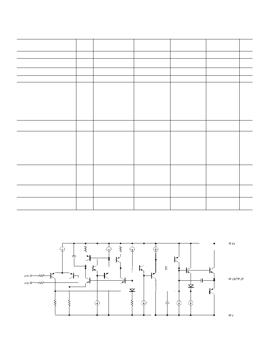
SIMPLIFIED SCHEMATIC
(@ V
S
= 1.5 V to 15 V, 25 C
T
A
+85 C for OP490E/F, 40 C
T
A
+85 C for
OP490G, unless otherwise noted)
OP490
REV. B
5
Wafer Test Limits
Parameter
Symbol
Conditions
Limits
Units
Input Offset Voltage
V
OS
0.75
mV max
Input Offset Current
I
OS
V
CM
= 0 V
5
nA max
Input Bias Current
I
B
V
CM
= 0 V
20
nA max
Large Signal Voltage Gain
A
VO
V
S
=
±
15 V, V
O
=
±
10 V
R
L
= 100 k
500
V/mV min
R
L
= 10 k
250
V+ = 5 V, V = 0 V
125
V/mV min
1 V < V
O
< 4 V, R
L
= 100 k
Input Voltage Range
IVR
V+ = 5 V, V = 0 V
0/4
V min
V
S
=
±
15 V
1
15/13.5
Output Voltage Swing
V
S
=
±
15 V
V
O
R
L
= 10 k
±
13.5
V min
R
L
= 2 k
±
10.5
V
OH
V+ = 5 V, V = 0 V
R
L
= 2 k
4.0
V min
V
OL
V+ = 5 V, V = 0 V
R
L
= 10 k
500
µ
V max
Common-Mode Rejection
CMR
V+ = 5 V, V = 0 V, 0 V < V
CM
< 4 V
80
dB min
V
S
=
±
15 V, 15 V < V
CM
< 13.5 V
90
Power Supply Rejection Ratio
PSRR
10
µ
V/V max
Supply Current (All Amplifiers)
I
SY
V
S
=
±
15 V, No Load
80
µ
A max
NOTES
1
Guaranteed by CMR test.
Electrical tests are performed at wafer probe to the limits shown. Due to variations in assembly methods and normal yield loss, yield after packaging is not guaranteed
for standard product dice. Consult factory to negotiate specifications based on dice lot qualifications through sample lot assembly and testing.
(@ V
S
=
1.5 V to 15 V, T
A
= +25 C, unless otherwise noted)
ABSOLUTE MAXIMUM RATINGS
1
Supply Voltage . . . . . . . . . . . . . . . . . . . . . . . . . . . . . . .
±
18 V
Differential Input Voltage . . . . [(V) 20 V] to [(V+) + 20 V]
Common-Mode Input Voltage . [(V) 20 V] to [(V+) + 20 V]
Output Short-Circuit Duration . . . . . . . . . . . . . . . Continuous
Storage Temperature Range
TC, Y, P Package . . . . . . . . . . . . . . . . . . . 65
°
C to +150
°
C
Operating Temperature Range
OP490A . . . . . . . . . . . . . . . . . . . . . . . . . . 55
°
C to +125
°
C
OP490E, OP490F . . . . . . . . . . . . . . . . . . . 25
°
C to +85
°
C
OP490G . . . . . . . . . . . . . . . . . . . . . . . . . . . 40
°
C to +85
°
C
Junction Temperature (T
J
) . . . . . . . . . . . . . 65
°
C to +150
°
C
Lead Temperature Range (Soldering, 60 sec) . . . . . . +300
°
C
Package Type
JA
2
JC
Units
14-Pin Hermetic DIP (Y)
99
12
°
C/W
14-Pin Plastic DIP (P)
76
33
°
C/W
28-Contact LCC (TC)
78
30
°
C/W
16-Pin SOL (S)
92
27
°
C/W
NOTES
1
Absolute maximum ratings apply to both DICE and packaged parts, unless
otherwise noted.
2
JA
is specified for worst case mounting conditions, i.e.,
JA
is specified for device
in socket for Cerdip, P-DIP, and LCC packages;
JA
is specified for device soldered
to printed circuit board for SOL package.
ORDERING GUIDE
1
T
A
= +25 C
Operating
V
OS
max
Temperature
Package
Model
(mV)
Range
Description
OP490AY
2
0.5
MIL
14-Pin Cerdip
OP490ATC/883
0.5
MIL
28-Contact LCC
OP490EY
0.5
IND
14-Pin Cerdip
OP490FY
0.75
IND
14-Pin Cerdip
OP490GP
1.0
XIND
14-Pin Plastic DIP
OP490GS
3
1.0
XIND
16-Pin SOL
NOTES
1
Burn-in is available on commercial and industrial temperature range parts in
cerdip, plastic DIP and TO-can packages.
2
For devices processed in total compliance to MIL-STD-883, add /883 after
part number. Consult factory for 883 data sheet.
3
For availability and burn-in information on SO and PLCC packages, contact
your local sales office.
DICE CHARACTERISTICS
Die Size 0.139
×
0.121 inch, 16,819 sq. mils
(3.53
×
3.07 mm, 10.84 sq. mm)
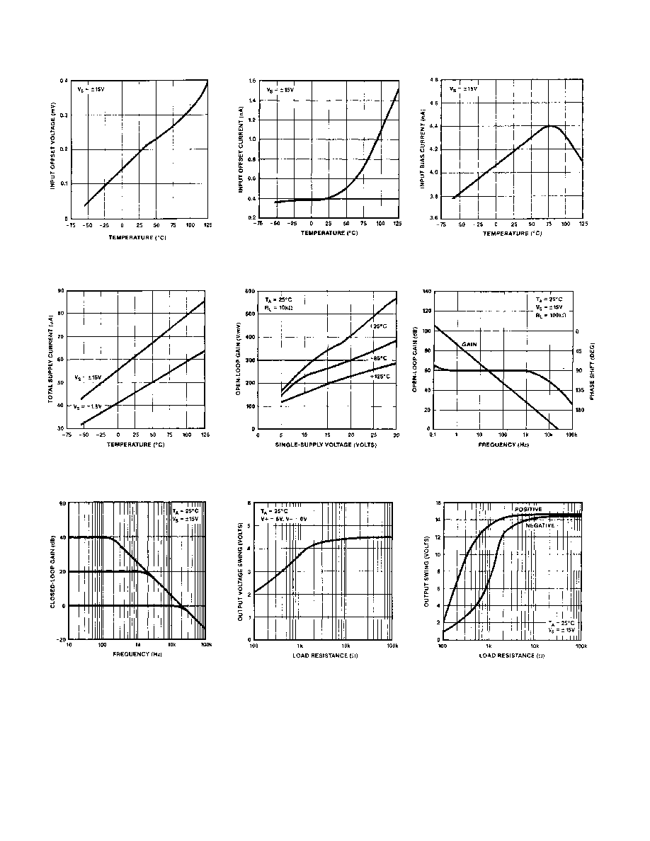
OP490Typical Performance Characteristics
REV. B
6
Input Offset Current
vs. Temperature
Open-Loop Gain vs.
Single-Supply Voltage
Output Voltage Swing
vs. Load Resistance
Input Offset Voltage
vs. Temperature
Total Supply Current
vs. Temperature
Closed-Loop Gain
vs. Frequency
Input Bias Current
vs. Temperature
Open-Loop Gain and
Phase Shift vs. Frequency
Output Voltage Swing
vs. Load Resistance
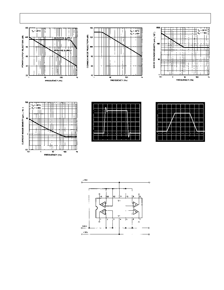
OP490
REV. B
7
Power Supply Rejection
vs. Frequency
Current Noise Density
vs. Frequency
Common-Mode Rejection
vs. Frequency
10
0%
100µs
20mV
100
90
T
A
= 25
°
C
V
S
=
±
15V
A
V
= +1
R
L
= 10k
C
L
= 500pF
Small-Signal
Transient Response
Noise Voltage Density
vs. Frequency
10
0%
1ms
5V
100
90
T
A
= 25
°
C
V
S
=
±
15V
A
V
= +1
R
L
= 10k
C
L
= 500pF
Large-Signal
Transient Response
Burn-In Circuit
OP490
REV. B
8
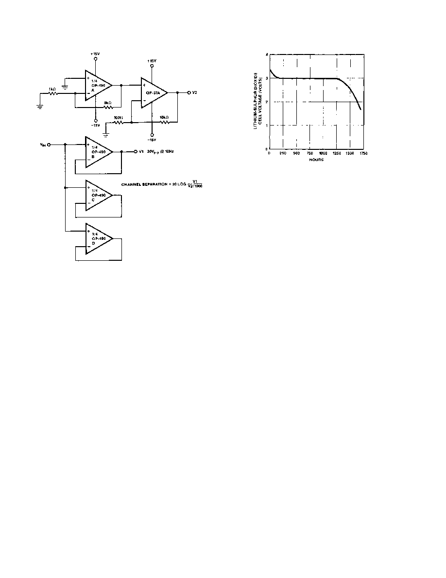
Figure 1. Lithium-Sulphur Dioxide Cell Discharge Charac-
teristic with OP490 and 100 k
Loads
requirement of the OP490, combined with the flat discharge
characteristic of the lithium cell, indicates that the OP490 can
be operated over the entire useful life of the cell. Figure 1 shows
the typical discharge characteristic of a 1 Ah lithium cell power-
ing an OP490 with each amplifier, in turn, driving full output
swing into a 100 k
load.
SINGLE-SUPPLY OUTPUT VOLTAGE RANGE
In single-supply operation the OP490's input and output ranges
include ground. This allows true "zero-in, zero-out" operation.
The output stage provides an active pull-down to around 0.8 V
above ground. Below this level, a load resistance of up to 1 M
to ground is required to pull the output down to zero.
In the region from ground to 0.8 V the OP490 has voltage gain
equal to the data sheet specification. Output current source ca-
pability is maintained over the entire voltage range including
ground.
INPUT VOLTAGE PROTECTION
The OP490 uses a PNP input stage with protection resistors in
series with the inverting and noninverting inputs. The high
breakdown of the PNP transistors coupled with the protection
resistors provides a large amount of input protection, allowing
the inputs to be taken 20 V beyond either supply without dam-
aging the amplifier.
Channel Separation Test Circuit
APPLICATIONS INFORMATION
BATTERY-POWERED APPLICATIONS
The OP490 can be operated on a minimum supply voltage of
+1.6 V, or with dual supplies of
±
0.8 V, and draws only 60
µ
A
of supply current. In many battery-powered circuits, the OP490
can be continuously operated for hundreds of hours before re-
quiring battery replacement, reducing equipment downtime and
operating costs.
High performance portable equipment and instruments fre-
quently use lithium cells because of their long shelf-life, light
weight, and high energy density relative to older primary cells.
Most lithium cells have a nominal output voltage of 3 V and are
noted for a flat discharge characteristic. The low supply current
OP490
REV. B
9
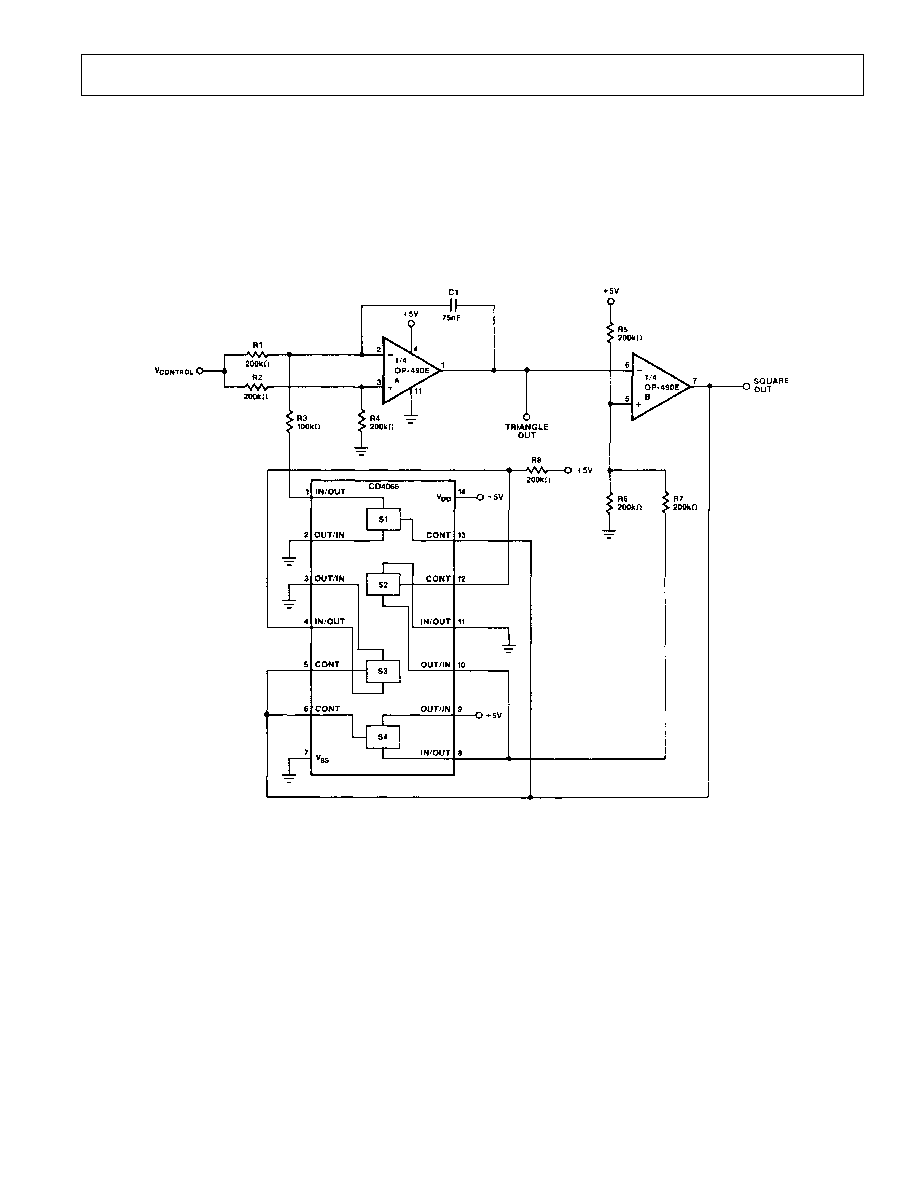
MICROPOWER VOLTAGE-CONTROLLED OSCILLATOR
An OP490 in combination with an inexpensive quad CMOS
switch comprise the precision V
CO
of Figure 2. This circuit pro-
vides triangle and square wave outputs and draws only 75
µ
A
from a 5 V supply. A acts as an integrator; S1 switches the
charging current symmetrically to yield positive and negative
ramps. The integrator is bounded by B which acts as a Schmitt
trigger with a precise hysteresis of 1.67 volts, set by resistors R5,
R6, and R7, and associated CMOS switches. The resulting out-
put of A is a triangle wave with upper and lower levels of 3.33
and 1.67 volts. The output of B is a square wave with almost
rail-to-rail swing. With the components shown, frequency of op-
eration is given by the equation:
f
OUT
=
V
CONTROL
(Volts)
×
10 Hz/V
but this is easily changed by varying C1. The circuit operates
well up to a few hundred hertz.
Figure 2. Micropower Voltage Controlled Oscillator
OP490
REV. B
10
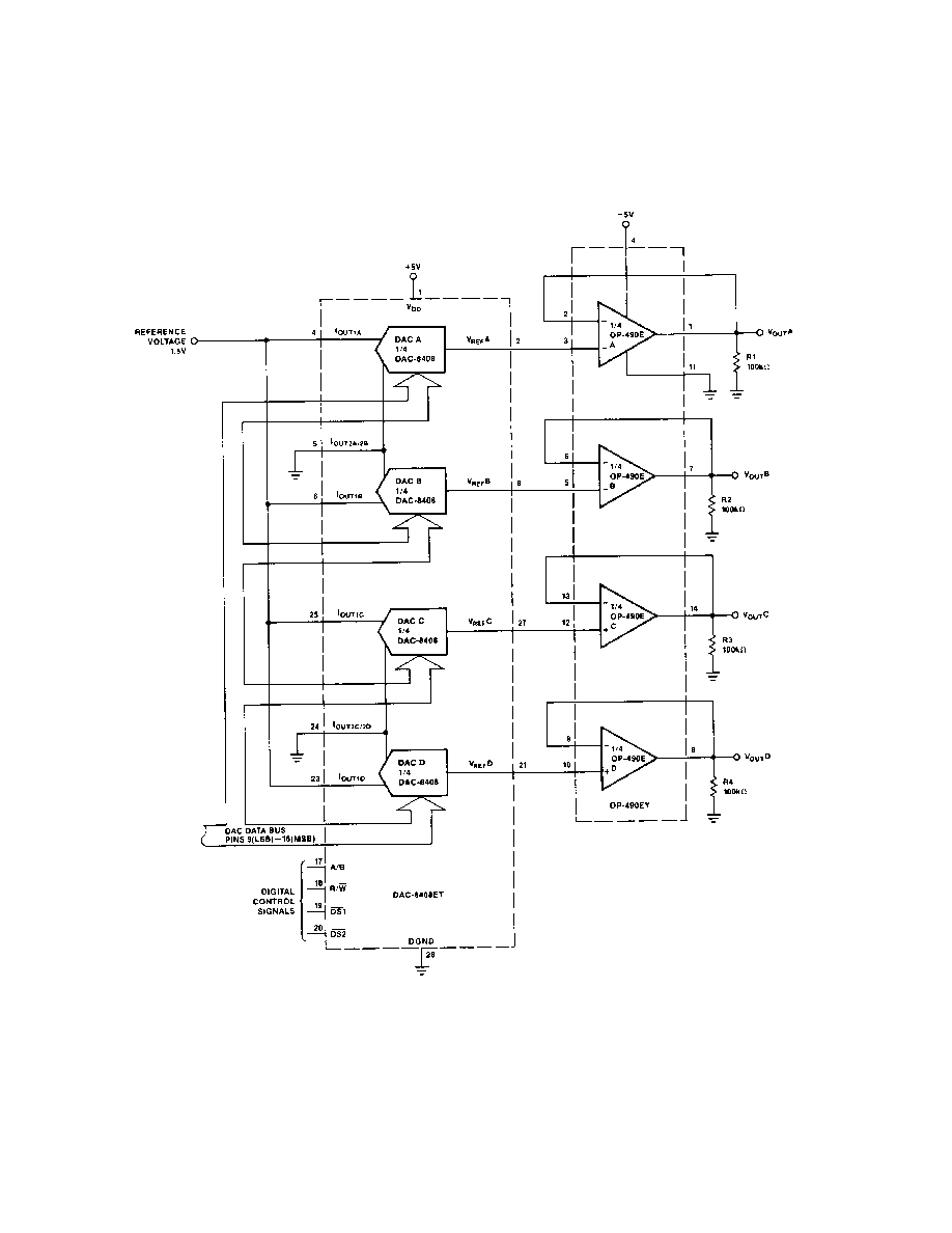
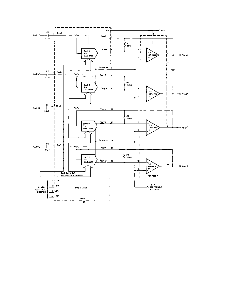
MICROPOWER SINGLE-SUPPLY
QUAD VOLTAGE-OUTPUT 8-BIT DAC
The circuit of Figure 3 uses the DAC8408 CMOS quad 8-bit
DAC, and the OP490 to form a single-supply quad voltage-out-
put DAC with a supply drain of only 140
µ
A. The DAC8408 is
used in voltage switching mode and each DAC has an output re-
sistance (
10 k
) independent of the digital input code. The
output amplifiers act as buffers to avoid loading the DACs. The
100 k
resistors ensure that the OP490 outputs will swing be-
low 0.8 V when required.
Figure 3. Micropower Single-Supply Quad Voltage Output 8-Bit DAC
OP490
REV. B
11
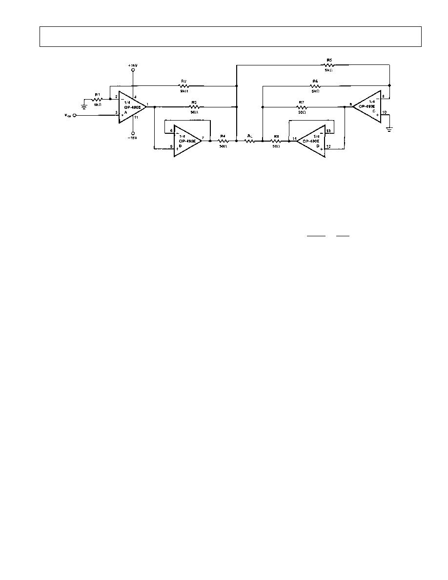
Figure 4. High Output Amplifier
HIGH OUTPUT AMPLIFIER
The amplifier shown in Figure 4 is capable of driving 25 V p-p
into a 1 k
load. Design of the amplifier is based on a bridge
configuration. A amplifies the input signal and drives the load
with the help of B. Amplifier C is a unity-gain inverter which
drives the load with help from D. Gain of the high output am-
plifier with the component values shown is 10, but can easily be
changed by varying R1 or R2.
SINGLE-SUPPLY MICROPOWER QUAD
PROGRAMMABLE GAIN AMPLIFIER
The combination of quad OP490 and the DAC8408 quad 8-bit
CMOS DAC, creates a quad programmable-gain amplifier with
a quiescent supply drain of only 140
µ
A. The digital code
present at the DAC, which is easily set by a microprocessor, de-
termines the ratio between the fixed DAC feedback resistor and
the resistance of the DAC ladder presents to the op amp feed-
back loop. Gain of each amplifier is:
V
OUT
V
IN
=
256
n
where n equals the decimal equivalent of the 8-bit digital code
present at the DAC. If the digital code present at the DAC con-
sists of all zeros, the feedback loop will be open causing the op
amp output to saturate. The 10 M
resistors placed in parallel
with the DAC feedback loop eliminates this problem with a very
small reduction in gain accuracy. The 2.5 V reference biases the
amplifiers to the center of the linear region providing maximum
output swing.
OP490
REV. B
12
PRINTED IN U.S.A.
Figure 5. Single Supply Micropower Quad Programmable Gain Amplifier