Äîêóìåíòàöèÿ è îïèñàíèÿ www.docs.chipfind.ru
MLT04
FUNCTIONAL BLOCK DIAGRAM
18-Lead Epoxy DIP (P Suffix)
18-Lead Wide Body SOIC (S Suffix)
REV. B
GENERAL DESCRIPTION
The MLT04 is a complete, four-channel, voltage output analog
multiplier packaged in an 18-pin DIP or SOIC-18. These complete
multipliers are ideal for general purpose applications such as voltage
controlled amplifiers, variable active filters, "zipper" noise free
audio level adjustment, and automatic gain control. Other applica-
tions include cost-effective multiple-channel power calculations
(I
×
V), polynomial correction generation, and low frequency
modulation. The MLT04 multiplier is ideally suited for generating
complex, high-order waveforms especially suitable for geometry
correction in high-resolution CRT display systems.
FEATURES
Four Independent Channels
Voltage IN, Voltage OUT
No External Parts Required
8 MHz Bandwidth
Four-Quadrant Multiplication
Voltage Output; W = (X
×
Y)/2.5 V
0.2% Typical Linearity Error on X or Y Inputs
Excellent Temperature Stability: 0.005%
±
2.5 V Analog Input Range
Operates from
±
5 V Supplies
Low Power Dissipation: 150 mW typ
Spice Model Available
APPLICATIONS
Geometry Correction in High-Resolution CRT Displays
Waveform Modulation & Generation
Voltage Controlled Amplifiers
Automatic Gain Control
Modulation and Demodulation
Fabricated in a complementary bipolar process, the MLT04
includes four 4-quadrant multiplying cells which have been laser-
trimmed for accuracy. A precision internal bandgap reference
normalizes signal computation to a 0.4 scale factor. Drift over
temperature is under 0.005%/
°
C. Spot noise voltage of 0.3
µ
V/
Hz
results in a THD + Noise performance of 0.02% (LPF = 22 kHz)
for the lower distortion Y channel. The four 8 MHz channels
consume a total of 150 mW of quiescent power.
The MLT04 is available in 18-pin plastic DIP, and SOIC-18
surface mount packages. All parts are offered in the extended
industrial temperature range (40
°
C to +85
°
C).
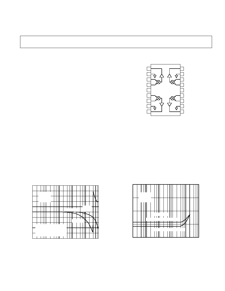
Figure 2. THD + Noise vs. Frequency
Figure 1. Gain & Phase vs. Frequency Response
100
1
0.01
10
100
1M
100k
10k
1k
0.1
10
FREQUENCY Hz
THD + NOISE %
V
CC
= +5V
V
EE
= 5V
T
A
= +25°C
THDX: X = 2.5VP, Y = +2.5V DC
THDY: Y = 2.5VP, X = +2.5V DC
LPF = 500kHz
1
2
3
4
5
6
7
8
9
18
17
16
15
14
13
12
11
10
MLT-04
18
17
16
15
14
13
12
11
10
4
1
2
3
5
6
7
8
9
MLT04
W4
GND4
X4
V
EE
Y4
Y3
X3
GND3
W3
W1
GND1
X1
Y1
V
CC
Y2
X2
GND2
W2
W = (X
·
Y)/2.5V
Av GAIN dB
0
1k
10k
100M
10M
1M
100k
20
40
40
20
FREQUENCY Hz
0
90
90
Ø Phase Degrees
V
CC
= +5V
V
EE
= 5V
T
A
= +25
°
C
X & Y MEASUREMENTS
SUPERIMPOSED:
X = 100mV RMS, Y = 2.5V DC
Y = 100mV RMS, X = 2.5V DC
Av (X OR Y)
Ø (X OR Y)
8.9MHz
3dB
One Technology Way, P.O. Box 9106, Norwood. MA 02062-9106, U.S.A.
Tel: 617/329-4700
Fax: 617/326-8703
a
Information furnished by Analog Devices is believed to be accurate and
reliable. However, no responsibility is assumed by Analog Devices for its
use, nor for any infringements of patents or other rights of third parties
which may result from its use. No license is granted by implication or
otherwise under any patent or patent rights of Analog Devices.
Four-Channel, Four-Quadrant
Analog Multiplier

ORDERING INFORMATION*
Temperature
Package
Package
Model
Range
Description
Option
MLT04GP
40
°
C to +85
°
C
18-Pin P-DIP
N-18
MLT04GS
40
°
C to +85
°
C
18-Lead SOIC SOL-18
MLT04GS-REEL
40
°
C to +85
°
C
18-Lead SOIC SOL-18
MLT04GBC
+25
°
C
Die
*For die specifications contact your local Analog sales office. The MLT04
contains 211 transistors.
(V
CC
= +5 V, V
EE
= 5 V, V
IN
=
±
2.5 V
P
, R
L
= 2 k
, T
A
= +25
°
C unless otherwise noted.)
2
MLT04SPECIFICATIONS
Parameter
Symbol
Conditions
Min
Typ
Max
Units
MULTIPLIER PERFORMANCE
1
Total Error
2
X
E
X
2.5 V < X < +2.5 V, Y = +2.5 V
5
±
2
5
% FS
Total Error
2
Y
E
Y
2.5 V < Y < +2.5 V, X = +2.5 V
5
±
2
5
% FS
Linearity Error
2
X
LE
X
2.5 V < X < +2.5 V, Y = +2.5 V
1
±
0.2
+1
% FS
Linearity Error
2
Y
LE
Y
2.5 V < Y < +2.5 V, X = +2.5 V
1
±
0.2
+1
% FS
Total Error Drift
TCE
X
X = 2.5 V, Y = 2.5 V, T
A
= 40
°
C to +85
°
C
0.005
%/
°
C
Total Error Drift
TCE
Y
Y = 2.5 V, X = 2.5 V, T
A
= 40
°
C to +85
°
C
0.005
%/
°
C
Scale Factor
3
K
X =
±
2.5 V, Y =
±
2.5 V, T
A
= 40
°
C to +85
°
C
0.38
0.40
0.42
1/V
Output Offset Voltage
Z
OS
X = 0 V, Y = 0 V, T
A
= 40
°
C to +85
°
C
50
±
10
50
mV
Output Offset Drift
TCZ
OS
X = 0 V, Y = 0 V, T
A
= 40
°
C to +85
°
C
50
µ
V/
°
C
Offset Voltage, X
X
OS
X = 0 V, Y =
±
2.5 V, T
A
= 40
°
C to +85
°
C
50
±
10.5
50
mV
Offset Voltage, Y
Y
OS
Y = 0 V, X =
±
2.5 V, T
A
= 40
°
C to +85
°
C
50
±
10.5
50
mV
DYNAMIC PERFORMANCE
Small Signal Bandwidth
BW
V
OUT
= 0.1 V rms
8
MHz
Slew Rate
SR
V
OUT
=
±
2.5 V
30
53
V/
µ
s
Settling Time
t
S
V
OUT
=
2.5 V to 1% Error Band
1
µ
s
AC Feedthrough
FT
AC
X = 0 V, Y = 1 V rms @ f = 100 kHz
65
dB
Crosstalk @ 100 kHz
CT
AC
X = Y = 1 V rms Applied to Adjacent Channel
90
dB
OUTPUTS
Audio Band Noise
E
N
f = 10 Hz to 50 kHz
76
µ
V rms
Wide Band Noise
E
N
Noise BW = 1.9 MHz
380
µ
V rms
Spot Noise Voltage
e
N
f = 1 kHz
0.3
µ
V/
Hz
Total Harmonic Distortion
THD
X
f = 1 kHz, LPF = 22 kHz, Y = 2.5 V
0.1
%
THD
Y
f = 1 kHz, LPF = 22 kHz, X = 2.5 V
0.02
%
Open Loop Output Resistance
R
OUT
40
Voltage Swing
V
PK
V
CC
= +5 V, V
EE
= 5 V
±
3.0
±
3.3
V
P
Short Circuit Current
I
SC
30
mA
INPUTS
Analog Input Range
IVR
GND = 0 V
2.5
+2.5
V
Bias Current
I
B
X = Y = 0 V
2.3
10
µ
A
Resistance
R
IN
1
M
Capacitance
C
IN
3
pF
SQUARE PERFORMANCE
Total Square Error
E
SQ
X = Y = 1
5
% FS
POWER SUPPLIES
Positive Current
I
CC
V
CC
= 5.25 V, V
EE
= 5.25 V
15
20
mA
Negative Current
I
EE
V
CC
= 5.25 V, V
EE
= 5.25 V
15
20
mA
Power Dissipation
P
DISS
Calculated = 5 V
×
I
CC
+ 5 V
×
I
EE
150
200
mW
Supply Sensitivity
PSSR
X = Y = 0 V, V
CC
=
5% or V
EE
=
5%
10
mV/V
Supply Voltage Range
V
RANGE
For V
CC
& V
EE
±
4.75
±
5.25
V
REV. B
NOTES
1
Specifications apply to all four multipliers.
2
Error is measured as a percent of the
±
2.5 V full scale, i.e., 1% FS = 25 mV.
3
Scale Factor K is an internally set constant in the multiplier transfer equation W = K
×
X
×
Y.
Specifications subject to change without notice.
ABSOLUTE MAXIMUM RATINGS*
Supply Voltages V
CC
, V
EE
to GND
±
7 V
Inputs X
I
, Y
I
V
CC
, V
EE
Outputs W
I
V
CC
, V
EE
Operating Temperature Range
40
°
C to +85
°
C
Maximum Junction Temperature (T
J
max)
+150
°
C
Storage Temperature
65
°
C to +150
°
C
Lead Temperature (Soldering, 10 sec)
+300
°
C
Package Power Dissipation
(T
J
maxT
A
)/
JA
Thermal Resistance
JA
PDIP-18 (N-18)
74
°
C/W
SOIC-18 (SOL-18)
89
°
C/W
*Stresses above those listed under "Absolute Maximum Ratings" may cause perma-
nent damage to the device. This is a stress rating only and functional operation of
the device at these or any other conditions above those indicated in the operational
section of this specification are not implied.
3
REV. B
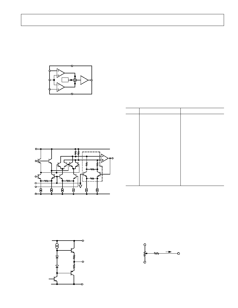
FUNCTIONAL DESCRIPTION
The MLT04 is a low cost quad, 4-quadrant analog multiplier with
single-ended voltage inputs and voltage outputs. The functional
block diagram for each of the multipliers is illustrated in Figure 3.
Due to packaging constraints, access to internal nodes for externally
adjusting scale factor, output offset voltage, or additional summing
signals is not provided.
Figure 3. Functional Block Diagram of Each MLT04
Multiplier
Each of the MLT04's analog multipliers is based on a Gilbert cell
multiplier configuration, a 1.23 V bandgap reference, and a unity-
connected output amplifier. Multiplier scale factor is determined
through a differential pair/trimmable resistor network external to
the core. An equivalent circuit for each of the multipliers is shown
in Figure 4.
Figure 4. Equivalent Circuit for the MLT04
Details of each multiplier's output-stage amplifier are shown in
Figure 5. The output stages idles at 200
µ
A, and the resistors in
series with the emitters of the output stage are 25
. The output
stage can drive load capacitances up to 500 pF without oscillation.
For loads greater than 500 pF, the outputs of the MLT04 should
be isolated from the load capacitance with a 100
resistor.
Figure 5. Equivalent Circuit for MLT04 Output Stages
ANALOG MULTIPLIER ERROR SOURCES
Multiplier errors consist primarily of input and output offsets, scale
factor errors, and nonlinearity in the multiplying core. An expres-
sion for the output of a real analog multiplier is given by:
V
O
=
( K
+
K ){(V
X
+
X
OS
)(V
Y
+
Y
OS
)
+
Z
OS
+
f ( X , Y )}
where:
K
=
Multiplier Scale Factor
K
=
Scale Factor Error
V
X
=
X-Input Signal
X
OS
=
X-Input Offset Voltage
V
Y
=
Y-Input Signal
Y
OS
=
Y-Input Offset Voltage
Z
OS
=
Multiplier Output Offset Voltage
(X, Y) =
Nonlinearity
Executing the algebra to simplify the above expression yields
expressions for all the errors in an analog multiplier:
Term
Description
Dependence on Input
KV
X
V
Y
True Product
Goes to Zero As Either or
Both Inputs Go to Zero
KV
Y
V
Y
Scale-Factor Error
Goes to Zero at V
X
, V
Y
= 0
V
X
Y
OS
Linear "X" Feedthrough
Proportional to V
X
Due to Y-Input Offset
V
Y
X
OS
Linear "Y" Feedthrough
Proportional to V
Y
Due to X-Input Offset
X
OS
Y
OS
Output Offset Due to X-,
Independent of V
X
, V
Y
Y-Input Offsets
Z
OS
Output Offset
Independent of V
X
, V
Y
(X, Y)
Nonlinearity
Depends on Both V
X
, V
Y
.
Contains Terms Dependent
on V
X
, V
Y
, Their Powers
and Cross Products
As shown in the table, the primary static errors in an analog
multiplier are input offset voltages, output offset voltage, scale
factor, and nonlinearity. Of the four sources of error, only two are
externally trimmable in the MLT04: the X- and Y-input offset
voltages. Output offset voltage in the MLT04 is factory-trimmed to
±
50 mV, and the scale factor is internally adjusted to
±
2.5% of full
scale. Input offset voltage errors can be eliminated by using the
optional trim circuit of Figure 6. This scheme then reduces the net
error to output offset, scale-factor (gain) error, and an irreducible
nonlinearity component in the multiplying core.
Figure 6. Optional Offset Voltage Trim Configuration
MLT04
V
CC
V
EE
W
OUT
25
25
V
CC
INTERNAL
BIAS
X
IN
GND
Y
IN
V
EE
W
OUT
22k
200µA
200µA
22k
22k
200µA
200µA
200µA
200µA
SCALE
FACTOR
50k
V
S
50k
+V
S
±100mV
FOR X
OS
, Y
OS
TRIM
CONNECT TO SUM
NODE OF AN EXT OP AMP
I
0.4
+V
S
V
S
X1, X2, X3, X4
G1, G2, G3, G4
Y1, Y2, Y3, Y4
W1, W2, W3, W4
MLT04

Figure 12. Y-Input Nonlinearity @ X = 2.5 V
Feedthrough
In the ideal case, the output of the multiplier should be zero if
either input is zero. In reality, some portion of the nonzero input
will "feedthrough" the multiplier and appear at the output. This is
caused by the product of the nonzero input and the offset voltage of
the "zero" input. Introducing an offset equal to and opposite of the
"zero" input offset voltage will null the linear component of the
feedthrough. Residual feedthrough at the output of the multiplier
is then irreducible core nonlinearity.
Typical X- and Y-input feedthrough curves for the MLT04 are
shown in Figures 7 and 8, respectively. These curves illustrate
MLT04 feedthrough after "zero" input offset voltage trim.
Residual X-input feedthrough measures 0.08% of full scale,
whereas residual Y-input feedthrough is almost immeasurable.
Figure 7. X-Input Feedthrough with Y
OS
Nulled
Figure 8. Y-Input Feedthrough with X
OS
Nulled
Nonlinearity
Multiplier core nonlinearity is the irreducible component of error.
It is the difference between actual performance and "best-straight-
line" theoretical output, for all pairs of input values. It is expressed
as a percentage of full scale with all other dc errors nulled. Typical
X- and Y-input nonlinearities for the MLT04 are shown in Figures
9 through 12. Worst-case X-input nonlinearity measured less than
0.2%, and Y-input nonlinearity measured better than 0.06%. For
modulator/demodulator or mixer applications it is, therefore,
recommended that the carrier be connected to the X-input while
the signal is applied to the Y-input.
REV. B
Figure 10. X-Input Nonlinearity @ Y = 2.5 V
Figure 11. Y-Input Nonlinearity @ X = +2.5 V
MLT04
Figure 9. X-Input Nonlinearity @ Y = +2.5 V
100
90
10
0%
VERTICAL 5mV/DIV
HORIZONTAL 0.5V/DIV
Y-INPUT: ±2.5V @ 10Hz
X
OS
NULLED
T
A
= +25°C
100
90
10
0%
VERTICAL 5mV/DIV
HORIZONTAL 0.5V/DIV
X-INPUT: ±2.5V @ 10Hz
Y-INPUT: +2.5V
Y
OS
NULLED
T
A
= +25°C
100
90
10
0%
VERTICAL 5mV/DIV
HORIZONTAL 0.5V/DIV
X-INPUT: ±2.5V @ 10Hz
Y
OS
NULLED
T
A
= +25°C
100
90
10
0%
VERTICAL 5mV/DIV
HORIZONTAL 0.5V/DIV
X-INPUT: ±2.5V @ 10Hz
Y-INPUT: 2.5V
Y
OS
NULLED
T
A
= +25°C
100
90
10
0%
VERTICAL 5mV/DIV
HORIZONTAL 0.5V/DIV
Y-INPUT: ±2.5V @ 10Hz
X-INPUT: +2.5V
X
OS
NULLED
T
A
= +25°C
100
90
10
0%
VERTICAL 5mV/DIV
HORIZONTAL 0.5V/DIV
Y-INPUT: ±2.5V @ 10Hz
X-INPUT: 2.5V
X
OS
NULLED
T
A
= +25°C
4

Typical Performance Characteristics MLT04
5
REV. B
Figure 16. X-Input Gain and Phase vs. Frequency
Figure 17. Y-Input Gain and Phase vs. Frequency
Figure 18. Amplitude Response vs. Capacitive Load
Figure 15. Noise Density vs. Frequency
10000
1000
0
100
NOISE DENSITY nV/
Hz
FREQUENCY Hz
10
100
1M
100k
10k
1k
V
S
= ±5V
T
A
= +25
°
C
10k
100k
10M
1M
12
12
0
6
6
9
3
3
9
180
0
90
90
135
45
45
135
180
T
A
= +25
°
C
V
S
= ±5V
V
X
= 100mV
V
Y
= +2.5V
GAIN
PHASE
PHASE = 68.3
°
@ 7.142 MHz
FREQUENCY Hz
GAIN
dB
PHASE Degrees
FREQUENCY Hz
1k
10k
100M
10M
1M
100k
8
2
12
0
2
4
6
10
8
6
4
AV GAIN dB
C
L
= 320pF
C
L
= 560pF
C
L
= 220pF
NO C
L
C
L
= 100pF
V
S
= ±5V
R
L
= 2k
T
A
= +25°C
Figure 13. Broadband Noise
OUTPUT NOISE VOLTAGE 100µV/DIV
TIME = 10ms/DIV
NBW = 10Hz 50kHz
T
A
= +25°C
100
10
0%
90
Figure 14. Broadband Noise
OUTPUT NOISE VOLTAGE 625µV/DIV
TIME = 10ms/DIV
NBW = 1.9MHz
T
A
= +25°C
100
10
0%
90
10k
100k
10M
1M
12
12
0
6
6
9
3
3
9
180
0
90
90
135
45
45
135
180
T
A
= +25
°
C
V
S
=
±
5V
V
X
= +2.5V
V
Y
= 100mV
GAIN
PHASE
PHASE = 68.1
°
@ 8.064 MHz
FREQUENCY Hz
GAIN
dB
PHASE D
egrees