Äîêóìåíòàöèÿ è îïèñàíèÿ www.docs.chipfind.ru
REV. 0
Information furnished by Analog Devices is believed to be accurate and
reliable. However, no responsibility is assumed by Analog Devices for its
use, nor for any infringements of patents or other rights of third parties that
may result from its use. No license is granted by implication or otherwise
under any patent or patent rights of Analog Devices.
a
ADV7197
One Technology Way, P.O. Box 9106, Norwood, MA 02062-9106, U.S.A.
Tel: 781/329-4700
www.analog.com
Fax: 781/326-8703
© Analog Devices, Inc., 2001
Multiformat HDTV Encoder with
Three 11-Bit DACs
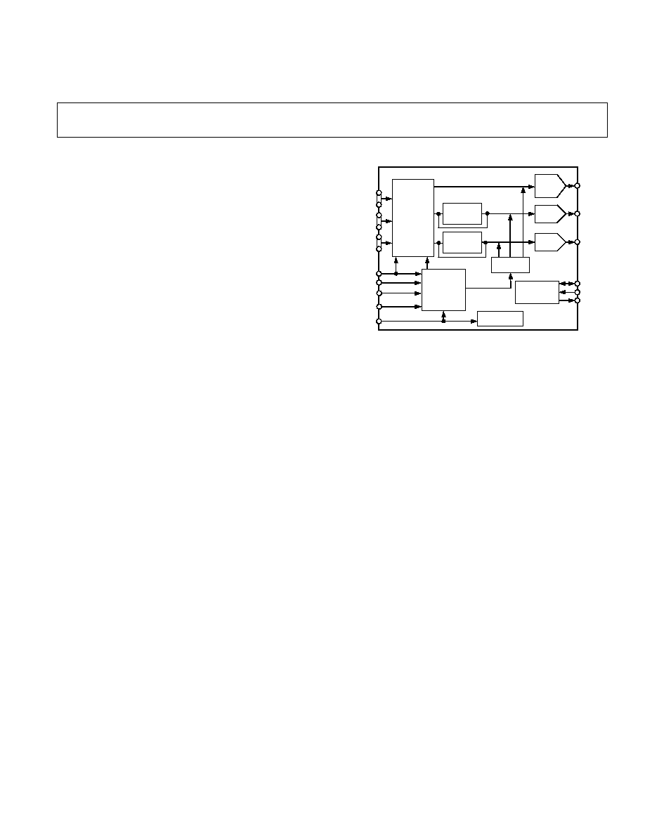
FUNCTIONAL BLOCK DIAGRAM
TEST
PATTERN
GENERATOR
AND
DELAY
Y0Y9
Cr0Cr9
Cb0Cb9
SYNC
GENERATOR
TIMING
GENERATOR
I
2
C MPU
PORT
CLKIN
HORIZONTAL
SYNC
VERTICAL
SYNC
BLANKING
RESET
ADV7197
DAC CONTROL
BLOCK
DAC A (Y)
DAC B
DAC C
V
REF
R
SET
COMP
11-BIT
+ SYNC
DAC
11-BIT
DAC
11-BIT
DAC
CHROMA
4:2:2 TO 4:4:4
(SSAF)
CHROMA
4:2:2 TO 4:4:4
(SSAF)
FEATURES
INPUT FORMATS
YCrCb in 2
10-Bit (4:2:2) or 3 10-Bit (4:4:4) Format
Compliant to SMPTE274M (1080i), SMPTE296M
(720p) and Any Other High-Definition Standard Using
Async Timing Mode
RGB in 3
10-Bit 4:4:4 Format
OUTPUT FORMATS
YPrPb HDTV (EIA-770.3)
RGB Levels Compliant to RS-170 and RS-343A
11-Bit + Sync (DAC A)
11-Bit DACs (DAC B, C)
PROGRAMMABLE FEATURES
Internal Test Pattern Generator with Color Control
Y/C Delay ( )
Individual DAC On/Off Control
VBI Open Control
I
2
C Filter
2-Wire Serial MPU Interface
Single Supply 5 V/3.3 V Operation
52-Lead MQFP Package
APPLICATIONS
HDTV Display Devices
HDTV Projection Systems
Digital Video Systems
High Resolution Color Graphics
Image Processing/Instrumentation
Digital Radio Modulation/Video Signal Reconstruction
*ADV is a registered trademark of Analog Devices, Inc.
GENERAL DESCRIPTION
The ADV7197 is a triple, high-speed, digital-to-analog encoder
on a single monolithic chip. It consists of three high-speed video
D/A converters with TTL-compatible inputs.
The ADV7197 has three separate 10-bit-wide input ports that
accept data in 4:4:4 10-bit YCrCb or RGB, or 4:2:2 10-bit
YCrCb. This data is accepted in HDTV format at 74.25 MHz
or 74.1758 MHz. For any other high definition standard but
SMPTE274M or SMPTE296M, the Async Timing Mode can
be used to input data to the ADV7197. For all standards,
external horizontal, vertical, and blanking signals or EAV/SAV
codes control the insertion of appropriate synchronization signals
into the digital data stream and therefore the output signals.
The ADV7197 outputs analog YPrPb HDTV complying to
EIA-770.3, or RGB complying to RS-170/RS-343A.
The ADV7197 requires a single 5 V/3.3 V power supply, an
optional external 1.235 V reference, and a 74.25 MHz (or
74.1758 MHz) clock.
The ADV7197 is packaged in a 52-lead MQFP package.

REV. 0
2
ADV7197SPECIFICATIONS
5 V SPECIFICATIONS
1
Parameter
Min
Typ
Max
Unit
Test Conditions
STATIC PERFORMANCE
Resolution
11
Bits
Integral Nonlinearity
1.5
LSB
Differential Nonlinearity
0.9
2.0
LSB
Guaranteed Monotonic
DIGITAL OUTPUTS
Output High Voltage, V
OH
2.4
V
I
SOURCE
= 400
µA
Output Low Voltage, V
OL
0.4
V
I
SINK
= 3.2 mA
Three-State Leakage Current
10
µA
V
IN
= 0.4 V
Three-State Output Capacitance
4
pF
DIGITAL AND CONTROL INPUTS
Input High Voltage, V
IH
2.0
V
Input Low Voltage, V
IL
0.8
V
Input Leakage Current
0
1
µA
V
IN
= 0.4 V or 2.4 V
Input Capacitance, C
IN
4
pF
ANALOG OUTPUTS
Full-Scale Output Current
3.92
4.25
4.56
mA
DAC A
2.54
2.83
3.11
mA
DAC B, C
Output Current Range
3.92
4.25
4.56
mA
DAC A
2.39
2.66
2.93
mA
DAC B, C
DAC-to-DAC Matching
1.4
%
DAC A, B, C
Output Compliance Range, V
OC
1.4
V
Output Impedance, R
OUT
100
k
Output Capacitance, C
OUT
7
pF
VOLTAGE REFERENCE (External and Internal)
Reference Range, V
REF
1.112
1.235
1.359
V
POWER REQUIREMENTS
I
DD
2
96
102
mA
With f
CLK
= 74.25 MHz
I
AA
3, 4
11
15
mA
Power Supply Rejection Ratio
0.01
%/%
NOTES
1
Guaranteed by characterization.
2
I
DD
or the circuit current is the continuous current required to drive the digital core.
3
I
AA
is the total current required to supply all DACs including V
REF
circuitry.
4
All DACs on.
Specifications subject to change without notice.
(V
AA
= 4.75 V to 5.25 V, V
REF
= 1.235 V, R
SET
= 2470
, R
LOAD
= 300
. All specifications T
MIN
to T
MAX
[0 C to
70 C] unless otherwise noted.)

REV. 0
3
ADV7197
3.3 V SPECIFICATIONS
1
Parameter
Min
Typ
Max
Unit
Test Conditions
STATIC PERFORMANCE
Resolution
11
Bits
Integral Nonlinearity
1.5
LSB
Differential Nonlinearity
0.9
2.0
LSB
DIGITAL OUTPUTS
Output High Voltage, V
OH
2.4
V
I
SOURCE
= 400
µA
Output Low Voltage, V
OL
0.4
V
I
SINK
= 3.2 mA
Three-State Leakage Current
10
µA
V
IN
= 0.4 V
Three-State Output Capacitance
4
pF
DIGITAL AND CONTROL INPUTS
Input High Voltage, V
IH
2
V
Input Low Voltage, V
IL
0.8
0.65
V
Input Leakage Current
0
1
µA
V
IN
= 0.4 V or = 2.4 V
Input Capacitance, C
IN
4
pF
ANALOG OUTPUTS
Full-Scale Output Current
3.92
4.25
4.56
mA
DAC A
2.54
2.83
3.11
mA
DAC B, C
Output Current Range
3.92
4.25
4.56
mA
DAC A
2.39
2.66
2.93
mA
DAC B, C
DAC-to-DAC Matching
1.4
%
DAC A, B, C
Output Compliance Range, V
OC
0
1.4
V
Output Impedance, R
OUT
100
k
Output Capacitance, C
OUT
7
pF
VOLTAGE REFERENCE (External)
Reference Range, V
REF
1.112
1.235
1.359
V
POWER REQUIREMENTS
I
DD
2
46
mA
With f
CLK
= 74.25 MHz
I
AA
3, 4
11
15
mA
Power Supply Rejection Ratio
0.01
%/%
NOTES
1
Guaranteed by characterization.
2
I
DD
or the circuit current is the continuous current required to drive the digital core.
3
I
AA
is the total current required to supply all DACs including V
REF
circuitry.
4
All DACs on.
Specifications subject to change without notice.
(V
AA
= 3.15 V to 3.45 V, V
REF
= 1.235 V, R
SET
= 2470
, R
LOAD
= 300
. All specifications T
MIN
to T
MAX
[0 C
to 70 C] unless otherwise noted.)
REV. 0
4
ADV7197SPECIFICATIONS
5 V DYNAMICSPECIFICATIONS
Parameter
Min
Typ
Max
Unit
Luma Bandwidth
13.5
MHz
Chroma Bandwidth
6.75
MHz
Signal-to-Noise Ratio
64
dB Luma Ramp Unweighted
Chroma/Luma Delay Inequality
0
ns
Specifications subject to change without notice.
3.3 V DYNAMICSPECIFICATIONS
Parameter
Min
Typ
Max
Unit
Luma Bandwidth
13.5
MHz
Chroma Bandwidth
6.75
MHz
Signal-to-Noise Ratio
64
dB Luma Ramp Unweighted
Chroma/Luma Delay Inequality
0
ns
Specifications subject to change without notice.
5 V TIMINGSPECIFICATIONS
P
arameter
Min
Typ
Max
Unit
Conditions
MPU PORT
1
SCLOCK Frequency
10
400
kHz
SCLOCK High Pulsewidth, t
1
0.6
µs
SCLOCK Low Pulsewidth, t
2
1.3
µs
Hold Time (Start Condition), t
3
0.6
µs
After This Period the 1st Clock Is Generated
Setup Time (Start Condition), t
4
0.6
µs
Relevant for Repeated Start Condition
Data Setup Time, t
5
100
ns
SDATA, SCLOCK Rise Time, t
6
300
ns
SDATA, SCLOCK Fall Time, t
7
300
ns
Setup Time (Stop Condition), t
8
0.6
µs
RESET Low Time
100
ns
ANALOG OUTPUTS
Analog Output Delay
2
10
ns
Analog Output Skew
0.5
ns
CLOCK CONTROL AND PIXEL PORT
3
f
CLK
74.25
MHz
HDTV Mode
t
CLK
81
MHz
Async Timing Mode
Clock High Time, t
9
5
1.5
ns
Clock Low Time, t
10
5
2.0
ns
Data Setup Time, t
11
2.0
ns
Data Hold Time, t
12
4.5
ns
Control Setup Time, t
11
7
ns
Control Hold Time, t
12
4.0
ns
Pipeline Delay
16
Clock Cycles
For 4:4:4 Pixel Input Format
NOTES
1
Guaranteed by characterization.
2
Output delay measured from the 50% point of the rising edge of CLOCK to the 50% point of DAC output full-scale transition.
3
Data: Cb/Cr (9:0), Cr (9:0), Y (9:0); Control:
HSYNC/SYNC, VSYNC/TSYNC; DV
Specifications subject to change without notice.
(V
AA
= 4.75 V to 5.25 V, V
REF
= 1.235 V, R
SET
= 2470
, R
LOAD
= 300
. All specifications T
MIN
to T
MAX
[0 C to 70 C] unless otherwise noted.)
(V
AA
= 3.15 V to 3.45 V, V
REF
= 1.235 V, R
SET
= 2470
, R
LOAD
= 300 . All specifications
T
MIN
to T
MAX
[0 C to 70 C] unless otherwise noted.)
(V
AA
= 4.75 V to 5.25 V, V
REF
= 1.235 V, R
SET
= 2470
, R
LOAD
= 300
. All specifications T
MIN
to T
MAX
[0 C to 70 C] unless otherwise noted.)
REV. 0
5
ADV7197
3.3 V TIMINGSPECIFICATIONS
P
arameter
Min
Typ
Max
Unit
Conditions
MPU PORT
1
SCLOCK Frequency
10
400
kHz
SCLOCK High Pulsewidth, t
1
0.6
µs
SCLOCK Low Pulsewidth, t
2
1.3
µs
Hold Time (Start Condition), t
3
0.6
µs
After This Period the 1st Clock Is Generated
Setup Time (Start Condition), t
4
0.6
µs
Relevant for Repeated Start Condition
Data Setup Time, t
5
100
ns
SDATA, SCLOCK Rise Time, t
6
300
ns
SDATA, SCLOCK Fall Time, t
7
300
ns
Setup Time (Stop Condition), t
8
0.6
µs
RESET Low Time
100
ns
ANALOG OUTPUTS
2
Analog Output Delay
10
ns
Analog Output Skew
0.5
ns
CLOCK CONTROL AND PIXEL PORT
3
f
CLK
74.25
MHz
HDTV Mode
t
CLK
81
MHz
Async Timing Mode
Clock High Time, t
9
5
1.5
ns
Clock Low Time, t
10
5
2.0
ns
Data Setup Time, t
11
2.0
ns
Data Hold Time, t
12
4.5
ns
Control Setup Time, t
11
7
ns
Control Hold Time, t
12
4.0
ns
Pipeline Delay
16
Clock Cycles
For 4:4:4 Pixel Input Format
NOTES
1
Guaranteed by characterization.
2
Output delay measured from the 50% point of the rising edge of CLOCK to the 50% point of DAC output full-scale transition.
3
Data: Cb/Cr (9:0), Cr (9:0), Y (9:0); Control:
HSYNC/SYNC, VSYNC/TSYNC; DV
Specifications subject to change without notice.
(V
AA
= 3.15 V to 3.45 V, V
REF
= 1.235 V, R
SET
= 2470
, R
LOAD
= 300 . All specifications
T
MIN
to T
MAX
[0 C to 70 C] unless otherwise noted.)
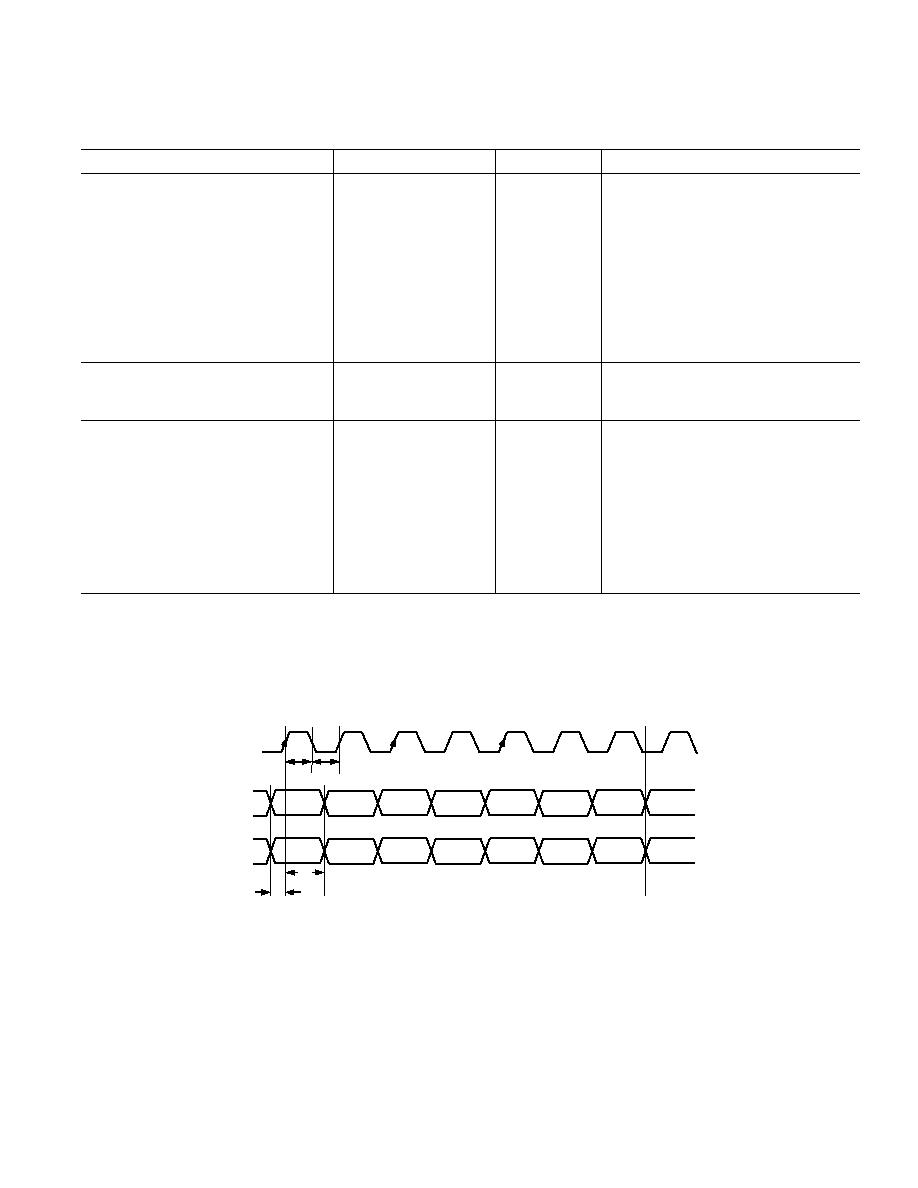
CLOCK
PIXEL INPUT
DATA
Y0
Cb0
Y1
Cr0
Y2
Cb1
Cr1
...
...
...
Yxxx
Cbxxx
Yxxx
Crxxx
t
11
t
12
t
9
t
10
t
9 CLOCK HIGH TIME
t
10 CLOCK LOW TIME
t
11 DATA SETUP TIME
t
12 DATA HOLD TIME
Figure 1. 4:2:2 Input Data Format Timing Diagram
Document Outline
- Specifications
- Pinout
- Package Drawings
- ORDERING GUIDE
- Features
- Applications
- Product Description
- Absolute Maximum Ratings
- Functional Block Diagram
- Pin Function Description
- CAUTION
- FUNCTIONAL DESCRIPTION
- MPU PORT DESCRIPTION
- REGISTER ACCESSES
- REGISTER PROGRAMMING
- MODE REGISTER 0
- MR0 (MR07-MR00)
- MR0 BIT DESCRIPTION
- MR1 (MR17-MR10)
- MODE REGISTER 2
- MR1 (MR27-MR20) MR3 (MR37-MR30)
- MR2 BIT DESCRIPTION
- MR4 (MR47-MR40)
- MR4 BIT DESCRIPTION
- MR5 BIT DESCRIPTION
- REGISTER SETTINGS REGISTER SETTINGS
- DIAGRAMS
- 2:2 Input Data Format Timing Diagram
- 4:4:4 YCrCb Input Data Format Timing Diagram
- 4:4:4 RGB Input Data Format Timing Diagram
- Input Timing Diagram
- MPU Port Timing Diagram
- Slave Address
- Bus Data Transfer
- Write and Read Sequence
- Subaddress Registers
- Async Timing ModeProgramming Input Control Signals for SMPTE295M Compatibility
- DV Input Control Signal in Relation to Video Output Signal for SMPTE296M (720p)
- Mode Register 0
- Mode Register 1
- Y and Color Delay
- Mode Register 2
- Mode Register 3
- Mode Register 4
- Mode Register 5
- Color Y Register
- Color Cr Register
- Color Cb Register
- Circuit Layout
- Output Buffer and Optional Filter
- EIA 770.3 Standard Output Signals (1080i, 720p)
- Output Levels for Full I/P Selection
- EAV/SAV Input Data Timing DiagramSMPTE274M (1080i)
- SMPTE296M (720p)
- SMPTE274M (1080i)