ADuM5240/ADuM5241/ADuM5242 Dual-Channel Isolators with Integrated DC/DC Converter, 50 mW Preliminary Data Sheet (Rev. PrI)
Dual-Channel Isolators with
Integrated DC/DC Converter, 50 mW
Preliminary Technical Data
ADuM5240/ADuM5241/ADuM5242
Rev. PrI
March 5, 2006
Information furnished by Analog Devices is believed to be accurate and reliable.
However, no responsibility is assumed by Analog Devices for its use, nor for any
infringements of patents or other rights of third parties that may result from its use.
Specifications subject to change without notice. No license is granted by implication
or otherwise under any patent or patent rights of Analog Devices. Trademarks and
registered trademarks are the property of their respective owners.
One Technology Way, P.O. Box 9106, Norwood, MA 02062-9106, U.S.A.
Tel: 781.329.4700
www.analog.com
Fax: 781.326.8703
© 2006 Analog Devices, Inc. All rights reserved.
FEATURES
Integrated isolated DC/DC converter
Regulated 5V/10 mA output
Dual dc-to-10 Mbps (NRZ) signal isolation channels
Narrow body SOIC 8-lead package
High temperature operation: 105°C
Precise timing characteristics:
3 ns maximum pulse-width distortion
3 ns maximum channel-to-channel matching
70 ns maximum propagation delay
High common-mode transient immunity: > 25 kV/s
Safety and regulatory approvals (pending)
UL recognition
2500 V rms for 1 minute per UL 1577
CSA component acceptance notice #5A
VDE certificate of conformity
DIN EN 60747-5-2 (VDE 0884 Part 2): 2003-01
DIN EN 60950 (VDE 0805): 2001-12; DIN EN 60950: 2000
V
IORM
= 560 V peak
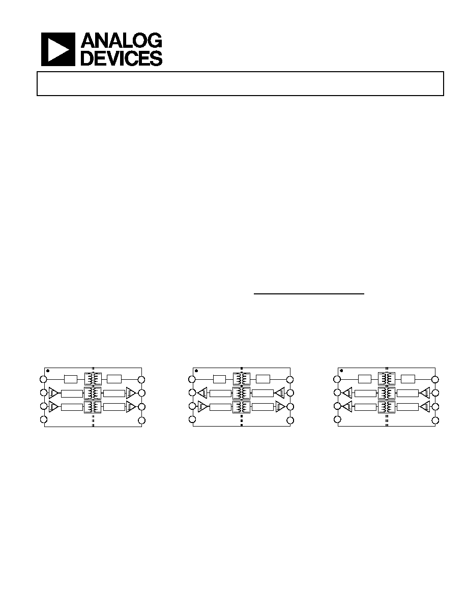
GENERAL DESCRIPTION
The ADuM524x
1
are dual-channel digital isolators having an
integrated DC/DC converter. Based on Analog Devices'
iCoupler® technology, the DC/DC converter provides up to
50 mW of regulated, isolated power at +5V. This eliminates the
need for a separate isolated DC/DC converter in low-power
isolated designs. Analog Devices' chip-scale transformer
iCoupler
®
technology is used both for the isolation of the logic
signals as well as for the DC/DC converter. The result is a small
form-factor total-isolation solution.
ADuM524x units may be used in combination or with other
iCoupler products to achieve higher output power levels or
greater channel counts.
The ADuM524x isolators provide two independent isolation
channels in a variety of channel configurations and data rates
(see Ordering Guide) operating off a 5V input supply.
1
Protected by U.S. Patents 5,952,849 and 6,873,065. Other patents pending.
FUNCTIONAL BLOCK DIAGRAM
GND
ISO
V
ISO
V
OA
7
V
OB
6
DECODE
ENCODE
DECODE
ENCODE
5
osc.
rect.
8
V
DD
GND
V
IA
2
V
IB
3
4
1
Figure 1. ADuM5240 Functional Block Diagram
GND
ISO
V
ISO
V
IA
7
V
OB
6
ENCODE
DECODE
DECODE
ENCODE
5
osc.
rect.
8
V
DD
GND
V
OA
2
V
IB
3
4
1
Figure 2. ADuM5241 Functional Block Diagram
GND
ISO
V
ISO
V
IA
7
V
IB
6
ENCODE
DECODE
ENCODE
DECODE
5
osc.
rect.
8
V
DD
GND
V
OA
2
V
OB
3
4
1
GND
ISO
V
ISO
V
IA
7
V
IB
6
ENCODE
DECODE
ENCODE
DECODE
5
osc.
rect.
8
V
DD
GND
V
OA
2
V
OB
3
4
1
Figure 3. ADuM5242 Functional Block Diagram

ADuM5240/ADuM5241/ADuM5242
Preliminary Technical Data
Rev. PrI | Page 2 of 10
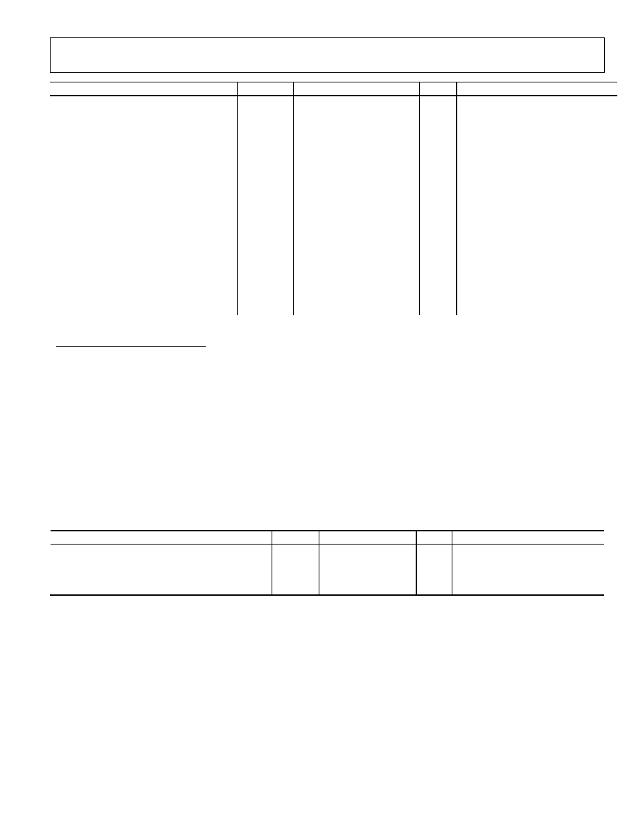
SPECIFICATIONS
ELECTRICAL CHARACTERISTICS
1
All voltages are relative to their respective ground. All min/max specifications apply over the entire recommended operating range,
unless otherwise noted. All typical specifications are at T
A
= 25°C, V
DD
= 5.0 V, V
ISO
= 5.25 V.
Table 1.
Parameter
Symbol
Min
Typ
Max
Unit
Test Conditions
With DC/DC Converter Enabled:
Output
Supply
Setpoint V
ISO
5.0
5.5
V
Maximum Output Current
DC to 2 Mbps
I
ISO(max, 2)
10
mA
Logic signal freq. 1 MHz
10 Mbps
I
ISO(max, 10)
5
mA
I
ISO
= 5 mA, Logic signal freq. = 5 MHz
ADuM5240
8.5
mA
ADuM5241
7.0
mA
ADum5242
5.7
mA
Input Supply Current
2
At Maximum Output Current, DC to 2 Mbps
I
DD(max)
115
mA
I
ISO
= 10 mA, Logic signal freq. 1 MHz
At Maximum Output Current, 10 Mbps
90
mA I
ISO
= 5 mA, Logic signal freq. = 5 MHz
With No Output Current
70
mA
I
ISO
= 0
With DC/DC Converter Disabled:
Input Supply Current, V
DD
2
DC to 2 Mbps
I
DD(2)
Logic signal freq.1 MHz
ADuM5240
3.3
mA
ADuM5241
2.7
mA
ADum5242
2.2
mA
10 Mbps
I
DD(10)
I
ISO
=0, Logic signal freq.5 MHz
ADuM5240
6.1
mA
ADuM5241
5.0
mA
ADum5242
3.6
mA
Input Supply Current, V
ISO
2
DC to 2 Mbps
I
ISO(2)
I
ISO
=0, Logic signal freq.1 MHz
ADuM5240
2.1
mA
ADuM5241
2.6
mA
ADum5242
3.0
mA
10 Mbps
I
ISO(10)
I
ISO
=0, Logic signal freq.5 MHz
ADuM5240
3.5
mA
ADuM5241
4.8
mA
ADum5242
6.0
mA
Enable Threshold
3
V
DISABLE
4.5 V
Disable Threshold
3
V
DISABLE
4.0 4.5
V
Input Currents
I
IA
, I
IB
-10
+0.01
+10
A
Logic High Input Threshold
V
IH
0.7 V
ISO
V
Logic Low Input Threshold
V
IL
0.3 V
ISO
V
Logic High Output Voltages
V
OAH
, V
OBH
V
DD
, - 0.1
5.0
V
I
Ox
= -20 A, V
Ix
= V
IxH
V
DD
, - 0.5
4.8
V
I
Ox
= -4 mA, V
Ix
= V
IxH
Logic Low Output Voltages
V
OAL
, V
OBL
0.0
0.1
V
I
Ox
= 20 A, V
Ix
= V
IxL
0.0
0.4
V
I
Ox
= 4 mA, V
Ix
= V
IxL
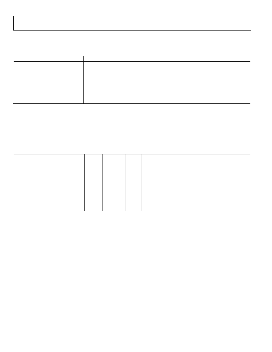
Preliminary Technical Data
ADuM5240/ADuM5241/ADuM5242
Rev. PrI | Page 3 of 10
Parameter
Symbol
Min
Typ
Max
Unit
Test Conditions
AC
SPECIFICATIONS
Minimum Pulse Width
4
PW
100
ns
C
L
= 15 pF, CMOS signal levels
Maximum Data Rate
5
10
Mbps
C
L
= 15 pF, CMOS signal levels
Propagation Delay
6
t
PHL
, t
PLH
25
70
ns
C
L
= 15 pF, CMOS signal levels
Pulse-Width Distortion, |t
PLH
- t
PHL
|
6
PWD
3
ns
C
L
= 15 pF, CMOS signal levels
Propagation Delay Skew
7
t
PSK
45
ns
C
L
= 15 pF, CMOS signal levels
Channel-to-Channel Matching,
Codirectional Channels
8
t
PSKCD
3 ns
C
L
= 15 pF, CMOS signal levels
Channel-to-Channel Matching,
Opposing-Directional Channels
9
t
PSKCD
15
ns
C
L
= 15 pF, CMOS signal levels
Enable Time
10
T
ENABLE
50
ns
Disable Time
10
T
DISABLE
50
ns
Output Rise/Fall Time (10% to 90%)
t
R
/t
F
2.5
ns
C
L
= 15 pF, CMOS signal levels
Common-Mode Transient Immunity
at Logic High Output
|CM
H
|
25
35
kV/s
V
Ix
= V
DD
, V
ISO
, V
CM
= 1000 V,
transient magnitude = 800 V
Common-Mode Transient Immunity
at Logic Low Output
|CM
L
|
25
35
kV/s
V
Ix
= 0 V, V = 1000 V,
transient magnitude = 800 V
Refresh Rate
f
r
1.0
Mbps
1
All voltages are relative to their respective ground.
2
Supply current values are specified with no load present on the digital outputs.
3
Enable/disable threshold is the voltage at which the internal DC/DC converter is enabled/disabled.
4
The minimum pulse width is the shortest pulse width at which the specified pulse-width distortion is guaranteed.
5
The maximum data rate is the fastest data rate at which the specified pulse-width distortion is guaranteed.
6
t
PHL
propagation delay is measured from the 50% level of the falling edge of the V
Ix
signal to the 50% level of the falling edge of the V
Ox
signal. t
PLH
propagation delay is
measured from the 50% level of the rising edge of the V
Ix
signal to the 50% level of the rising edge of the V
Ox
signal.
7
t
PSK
is the magnitude of the worst-case difference in t
PHL
and/or t
PLH
that is measured between units at the same operating temperature, supply voltages, and output
load within the recommended operating conditions.
8
Channel-to-channel matching is the absolute value of the difference in propagation delays between the two channels when operated with identical loads.
9
Channel-to-channel matching is the absolute value of the difference in propagation delays between the two channels when operated with identical loads.
10
Enable time is the duration from when input supply voltage rises above the enable threshold to when the internal DC/DC converter starts charging an external load.
Disable time is the duration from when the input supply voltage drops below the disable threshold to when the internal DC/DC converter stops charging an external
load
PACKAGE CHARACTERISTICS
Table 2.
Parameter
Symbol
Min
Typ
Max
Unit
Test Conditions
Resistance (Input-Output)
R
I-O
10
12
Capacitance (Input-Output)
C
I-O
1.0
pF
f = 1 MHz
Input Capacitance
C
I
4.0
pF
IC Junction-to-Air Thermal Resistance
JA
150
°C/W
ADuM5240/ADuM5241/ADuM5242
Preliminary Technical Data
Rev. PrI | Page 4 of 10
REGULATORY INFORMATION
The ADuM5240/5241/5242 will be approved by the following organizations upon product release:
Table 3.
UL (pending)
CSA (pending)
VDE (pending)
Recognized under 1577 Component
Recognition Program
1
Basic insulation, 2500 V rms isolation
rating
Approved under CSA Component
Acceptance Notice #5A
Basic insulation per CSA 60950-1-03
and IEC 60950-1, 400 V rms (560 V
peak) maximum working voltage
Certified according to
DIN EN 60747-5-2 (VDE 0884 Part 2):2003-01
2
Basic insulation,400 V rms (560 V peak) maximum
working voltage
File E214100
File 205078
File 2471900-4880-0001
1
In accordance with UL1577, each ADuM524x is proof-tested by applying an insulation test voltage 3000 V rms for 1 second (current leakage detection limit = 5 A).
2
In accordance with DIN EN 60747-5-2, each ADuM524x is proof-tested by applying an insulation test voltage 1050 V peak for 1 second (partial discharge detection
limit = 5 pC).
INSULATION AND SAFETY-RELATED SPECIFICATIONS
Table 4.
Parameter
Symbol Value
Unit
Conditions
Rated Dielectric Insulation Voltage
2500
V rms
1 minute duration
Minimum External Air Gap (Clearance)
L(I01)
4.90 min
mm
Measured from input terminals to output terminals, shortest
distance through air
Minimum External Tracking (Creepage)
L(I02)
4.01 min
mm
Measured from input terminals to output terminals, shortest
distance path along body
Minimum Internal Gap (Internal
Clearance)
0.017 min
mm
Insulation distance through insulation
Tracking Resistance (Comparative
Tracking Index)
CTI
>175
V
DIN IEC 112/VDE 0303 Part 1
Isolation Group
IIIa
Material Group (DIN VDE 0110, 1/89, Table 1)
Preliminary Technical Data
ADuM5240/ADuM5241/ADuM5242
Rev. PrI | Page 5 of 10
DIN EN 60747-5-2 (VDE 0884 PART 2) INSULATION CHARACTERISTICS
Table 5.
Description
Symbol Characteristic
Unit
Installation Classification per DIN VDE 0110
For Rated Mains Voltage 150 V rms
I-IV
For Rated Mains Voltage 300 V rms
I-III
For Rated Mains Voltage 400 V rms
I-II
Climatic Classification
40/105/21
Pollution Degree (DIN VDE 0110, Table 1)
2
Maximum Working Insulation Voltage
V
IORM
560
V peak
Input to Output Test Voltage, Method b1
V
PR
1050
V peak
V
IORM
× 1.875 = V
PR
, 100% Production Test, t
m
= 1 sec, Partial Discharge < 5 pC
Input to Output Test Voltage, Method a
V
PR
After Environmental Tests Subgroup 1
V
IORM
× 1.6 = V
PR
, t
m
= 60 sec, Partial Discharge < 5 pC
896
V peak
After Input and/or Safety Test Subgroup 2/3
V
IORM
× 1.2 = V
PR
, t
m
= 60 sec, Partial Discharge < 5 pC
672
V peak
Highest Allowable Overvoltage (Transient Overvoltage, t
TR
= 10 sec)
V
TR
4000
V peak
Safety-Limiting Values (maximum value allowed in the event of a failure; also see the thermal
derating curve, Figure 4)
Case Temperature
T
S
150
°C
Side 1 Current
I
S1
160
mA
Side 2 Current
I
S2
170
mA
Insulation Resistance at T
S
, V
IO
= 500 V
R
S
>10
9
Note that the "*" marking on the package denotes DIN EN 60747-5-2 approval for a 560 V peak working voltage.
This isolator is suitable for basic isolation only within the safety limit data. Maintenance of the safety data is ensured by protective circuits.
[Figure to be added]
Figure 4. Thermal Derating Curve, Dependence of Safety Limiting Values on
Case Temperature, per DIN EN 60747-5-2
RECOMMENDED OPERATING CONDITIONS
Table 6.
Parameter
Symbol
Min
Max
Unit
Operating Temperature
T
A
-40
+105
°C
Supply Voltages
1
V
DD
, DC/DC Conv. Enabled
V
DD
4.5
5.5
V
V
DD
, DC/DC Conv. Disabled
V
DD
2.7 4.0 V
V
ISO
, DC/DC Conv. Disabled
V
ISO
2.7 5.5 V
Input Signal Rise and Fall Times
1.0
ms
1
All voltages are relative to their respective ground.
ADuM5240/ADuM5241/ADuM5242
Preliminary Technical Data
Rev. PrI | Page 6 of 10
ABSOLUTE MAXIMUM RATINGS
Ambient temperature = 25°C, unless otherwise noted.
Table 7.
Parameter
Symbol
Min
Max
Unit
Storage Temperature
T
ST
-55
150
°C
Ambient Operating Temperature
T
A
-40
105
°C
Supply Voltages
1
V
DD
, V
ISO
-0.5
7.0
V
Input Voltage
1
V
IA
, V
IB
-0.5
V
DD/ISO
+ 0.5
V
Output Voltage
1
V
OA
, V
OB
-0.5
V
DD/ISO
+ 0.5
V
Average Output Current, per Pin
2
I
O
mA
Common-Mode Transients
3
-100
+100
kV/s
1
All voltages are relative to their respective ground.
2
See Figure 4 for maximum rated current values for various temperatures.
3
Refers to common-mode transients across the insulation barrier. Common-mode transients exceeding the Absolute Maximum Rating may cause latch-up or
permanent damage.
Stresses above those listed under Absolute Maximum Ratings may cause permanent damage to the device. This is a stress rating only;
Functional operation of the device at these or any other conditions above those listed in the operational sections of this specification is
not implied. Exposure to absolute maximum rating conditions for extended periods may affect device reliability.
ESD CAUTION
ESD (electrostatic discharge) sensitive device. Electrostatic charges as high as 4000 V readily accumulate on
the human body and test equipment and can discharge without detection. Although this product features
proprietary ESD protection circuitry, permanent damage may occur on devices subjected to high energy
electrostatic discharges. Therefore, proper ESD precautions are recommended to avoid performance
degradation or loss of functionality.
Table 8. Truth Table, ADuM5240
V
DD
State
DC/DC
Converter
V
ISO
State
V
IA
Input
V
IB
Input
V
OA
Output
V
OB
Output
Powered
Enabled
Powered
(Internally)
H
H
H
H
Powered
Enabled
Powered
(Internally)
L
L
L
L
Powered
Enabled
Powered
(Internally)
H
L
H
L
Powered
Enabled
Powered
(Internally)
L
H
L
H
Powered Disabled Powered
(Externally)
H H H H
Powered Disabled Powered
(Externally)
L
L
L
L
Powered Disabled Powered
(Externally)
H
L
H
L
Powered Disabled Powered
(Externally)
L
H
L
H
Powered
Disabled
Unpowered
X X Z Z
Unpowered Disabled
Powered
(Externally)
X X L L
Unpowered
Disabled
Unpowered
X X Z Z
Preliminary Technical Data
ADuM5240/ADuM5241/ADuM5242
Rev. PrI | Page 7 of 10
Table 9. Truth Table, ADuM5241
V
DD
State
DC/DC
Converter
V
ISO
State
V
IA
Input
V
IB
Input
V
OA
Output
V
OB
Output
Powered
Enabled
Powered
(Internally)
H
H
H
H
Powered
Enabled
Powered
(Internally)
L
L
L
L
Powered
Enabled
Powered
(Internally)
H
L
H
L
Powered
Enabled
Powered
(Internally)
L
H
L
H
Powered Disabled Powered
(Externally)
H H H H
Powered Disabled Powered
(Externally)
L
L
L
L
Powered Disabled Powered
(Externally)
H
L
H
L
Powered Disabled Powered
(Externally)
L
H
L
H
Powered
Disabled
Unpowered
X X L Z
Unpowered Disabled
Powered
(Externally)
X X Z L
Unpowered
Disabled
Unpowered
X X Z Z
Table 10. Truth Table, ADuM5242
V
DD
State
DC/DC
Converter
V
ISO
State
V
IA
Input
V
IB
Input
V
OA
Output
V
OB
Output
Powered
Enabled
Powered
(Internally)
H
H
H
H
Powered
Enabled
Powered
(Internally)
L
L
L
L
Powered
Enabled
Powered
(Internally)
H
L
H
L
Powered
Enabled
Powered
(Internally)
L
H
L
H
Powered Disabled Powered
(Externally)
H H H H
Powered Disabled Powered
(Externally)
L
L
L
L
Powered Disabled Powered
(Externally)
H
L
H
L
Powered Disabled Powered
(Externally)
L
H
L
H
Powered
Disabled
Unpowered
X X L L
Unpowered Disabled
Powered
(Externally)
X X Z Z
Unpowered
Disabled
Unpowered
X X Z Z
ADuM5240/ADuM5241/ADuM5242
Preliminary Technical Data
Rev. PrI | Page 8 of 10
PIN CONFIGURATION AND FUNCTION DESCRIPTIONS
TOP VIEW
(Not to Scale)
8
7
6
5
1
2
3
4
V
DD
V
IA
GND
V
ISO
V
OB
GND
ISO
ADuM5240
V
OA
V
IB
TOP VIEW
(Not to Scale)
8
7
6
5
1
2
3
4
V
DD
V
IA
GND
V
ISO
V
OB
GND
ISO
ADuM5240
V
OA
V
IB
Figure 5. ADuM5240 Pin Configuration
TOP VIEW
(Not to Scale)
8
7
6
5
1
2
3
4
V
DD
V
OA
GND
V
ISO
V
OB
GND
ISO
ADuM5241
V
IA
V
IB
TOP VIEW
(Not to Scale)
8
7
6
5
1
2
3
4
V
DD
V
OA
GND
V
ISO
V
OB
GND
ISO
ADuM5241
V
IA
V
IB
Figure 6. ADuM5241 Pin Configuration
TOP
V
IEW
(Not to Scale)
8
7
6
5
1
2
3
4
V
DD
V
OA
GND
V
ISO
V
IB
GND
ISO
ADuM
5242
V
IA
V
OB
Figure 7. ADuM5242 Pin Configuration
Table 11. ADuM5240 Pin Function Descriptions
Pin
No.
Mnemonic Function
1
V
DD1
Supply Voltage for Isolator Side 1,
4.5 V to 5.5 V (DC/DC Enabled), 2.7 V to 4.0
V (DC/DC Disabled)
2
V
IA
Logic Input A.
3
V
IB
Logic Input B.
4
GND
Ground. Ground reference for Isolator
Side 1.
5
GND
ISO
Isolated Ground. Ground reference for
Isolator Side 2.
6
V
OB
Logic Output B.
7
V
OA
Logic Output A.
8
V
ISO
Isolated Supply Voltage for Isolator Side 2,
5.0 V to 5.5 V Output (DC/DC Enabled), 4.5
V to 5.5 V Input (DC/DC Disabled)
Table 12. ADuM5241 Pin Function Descriptions
Pin
No.
Mnemonic Function
1
V
DD1
Supply Voltage for Isolator Side 1,
4.5 V to 5.5 V (DC/DC Enabled), 2.7 V to 4.0
V (DC/DC Disabled)
2
V
OA
Logic Output A.
3
V
IB
Logic Input B.
4
GND
Ground. Ground reference for Isolator
Side 1.
5
GND
ISO
Isolated Ground. Ground reference for
Isolator Side 2.
6
V
OB
Logic Output B.
7
V
IA
Logic Input A.
8
V
ISO
Isolated Supply Voltage for Isolator Side 2,
5.0 V to 5.5 V Output (DC/DC Enabled), 4.5
V to 5.5 V Input (DC/DC Disabled)
Table 13. ADuM5242 Pin Function Descriptions
Pin
No.
Mnemonic Function
1
V
DD1
Supply Voltage for Isolator Side 1,
4.5 V to 5.5 V (DC/DC Enabled), 2.7 V to 4.0
V (DC/DC Disabled)
2
V
OA
Logic Output A.
3
V
OB
Logic Output B.
4
GND
Ground. Ground reference for Isolator
Side 1.
5
GND
ISO
Isolated Ground. Ground reference for
Isolator Side 2.
6
V
IB
Logic Input B.
7
VI
A
Logic Input A.
8
V
ISO
Isolated Supply Voltage for Isolator Side 2,
5.0 V to 5.5 V Output (DC/DC Enabled), 4.5
V to 5.5 V Input (DC/DC Disabled)

Preliminary Technical Data
ADuM5240/ADuM5241/ADuM5242
Rev. PrI | Page 9 of 10
APPLICATION INFORMATION
The ADuM524x can be operated with the internal DC/DC
enabled or disabled. With the internal DC/DC converter
enabled, the Pin 8 isolated supply provides output power as well
as power to the part's isolated-side circuitry. Since the power
consumed by the ADuM524x is a function of the input signals'
data rate, the available isolated output power is determined by
the data rate at which the part's data channels are operating.
The ADuM524x's internal DC/DC converter state is controlled
by the input V
DD
voltage as defined in Table 6. In normal
operating mode, V
DD
is set between 4.5 V and 5.5 V and the
internal DC/DC converter is enabled. When/if it is desired to
disable the DC/DC converter, V
DD
is lowered to a value between
2.7 V and 4.0 V. In this mode, the V
ISO
supply is supplied by the
user and the ADuM524x's signal channels continue to operate
normally.
.
ADuM5240/ADuM5241/ADuM5242
Preliminary Technical Data
Rev. PrI | Page 10 of 10
OUTLINE DIMENSIONS
0.25 (0.0098)
0.17 (0.0067)
1.27 (0.0500)
0.40 (0.0157)
0.50 (0.0196)
0.25 (0.0099)
×
45°
8°
0°
1.75 (0.0688)
1.35 (0.0532)
SEATING
PLANE
0.25 (0.0098)
0.10 (0.0040)
4
1
8
5
5.00 (0.1968)
4.80 (0.1890)
4.00 (0.1574)
3.80 (0.1497)
1.27 (0.0500)
BSC
6.20 (0.2440)
5.80 (0.2284)
0.51 (0.0201)
0.31 (0.0122)
COPLANARITY
0.10
CONTROLLING DIMENSIONS ARE IN MILLIMETERS; INCH DIMENSIONS
(IN PARENTHESES) ARE ROUNDED-OFF MILLIMETER EQUIVALENTS FOR
REFERENCE ONLY AND ARE NOT APPROPRIATE FOR USE IN DESIGN
COMPLIANT TO JEDEC STANDARDS MS-012AA
Figure 8. 8-Lead Standard Small Outline Package [SOIC]--Narrow Body
(R-8)
Dimensions shown in millimeters (inches)
ORDERING GUIDE
Model
Number
of Inputs,
V
DD1
Side
Number
of Inputs,
V
DD2
Side
Maximum
Data Rate
(Mbps)
Temperature
Range (°C)
Package
Option
1
ADuM5240BRZ
2,3
2
0
10
-40 to +105
R-8
ADuM5241BRZ
2, 3
1
1
10
-40 to +105
R-8
ADuM5242BRZ
2, 3
0
2
10
-40 to +105
R-8
1
R-8 = 8-lead narrow body SOIC.
2
Tape and reel are available. The addition of an "-RL7" suffix designates a 7" (1,000 units) tape and reel option.
3
Z = Pb-free part.
PR06014-0-3/06(PrI)