Äîêóìåíòàöèÿ è îïèñàíèÿ www.docs.chipfind.ru
Quad-Channel Digital Isolators
ADuM1400/ADuM1401/ADuM1402
Rev. B
Information furnished by Analog Devices is believed to be accurate and reliable.
However, no responsibility is assumed by Analog Devices for its use, nor for any
infringements of patents or other rights of third parties that may result from its use.
Specifications subject to change without notice. No license is granted by implication
or otherwise under any patent or patent rights of Analog Devices. Trademarks and
registered trademarks are the property of their respective owners.
One Technology Way, P.O. Box 9106, Norwood, MA 02062-9106, U.S.A.
Tel: 781.329.4700
www.analog.com
Fax: 781.326.8703
© 2004 Analog Devices, Inc. All rights reserved.
FEATURES
Low power operation
5 V operation
1.0 mA per channel max @ 0 Mbps to 2 Mbps
3.5 mA per channel max @ 10 Mbps
31 mA per channel max @ 90 Mbps
3 V operation
0.7 mA per channel max @ 0 Mbps to 2 Mbps
2.1 mA per channel max @ 10 Mbps
20 mA per channel max @ 90 Mbps
Bidirectional communication
3 V/5 V level translation
High temperature operation: 105°C
High data rate: dc to 90 Mbps (NRZ)
Precise timing characteristics
2 ns max pulse-width distortion
2 ns max channel-to-channel matching
High common-mode transient immunity: >25 kV/s
Output enable function
Wide body 16-lead SOIC package, Pb-free models available
Safety and regulatory approvals
UL recognition: 2500 V rms for 1 minute per UL 1577
CSA component acceptance notice #5A
VDE certificate of conformity
DIN EN 60747-5-2 (VDE 0884 Part 2): 2003-01
DIN EN 60950 (VDE 0805): 2001-12; EN 60950: 2000
V
IORM
= 560 V peak
APPLICATIONS
General-purpose multichannel isolation
SPI® interface/data converter isolation
RS-232/RS-422/RS-485 transceiver
Industrial field bus isolation
GENERAL DESCRIPTION
The ADuM140x are 4-channel digital isolators based on Analog
Devices' iCoupler® technology. Combining high speed CMOS
and monolithic air core transformer technology, these isolation
components provide outstanding performance characteristics
superior to alternatives such as optocoupler devices.
By avoiding the use of LEDs and photodiodes, iCoupler devices
remove the design difficulties commonly associated with
optocouplers. The typical optocoupler concerns regarding
uncertain current transfer ratios, nonlinear transfer functions,
and temperature and lifetime effects are eliminated with the
simple iCoupler digital interfaces and stable performance
characteristics. The need for external drivers and other discretes
is eliminated with these iCoupler products. Furthermore,
iCoupler devices consumes one-tenth to one-sixth the power of
optocouplers at comparable signal data rates.
The ADuM140x isolators provide four independent isolation
channels in a variety of channel configurations and data rates
(see the Ordering Guide). All models operate with the supply
voltage on either side ranging from 2.7 V to 5.5 V, providing
compatibility with lower voltage systems as well as enabling a
voltage translation functionality across the isolation barrier. In
addition, the ADuM140x provides low pulse-width distortion
(<2 ns for CRW grade) and tight channel-to-channel matching
(<2 ns for CRW grade). Unlike other optocoupler alternatives,
the ADuM140x isolators have a patented refresh feature that
ensures dc correctness in the absence of input logic transitions
and during power-up/power-down conditions.
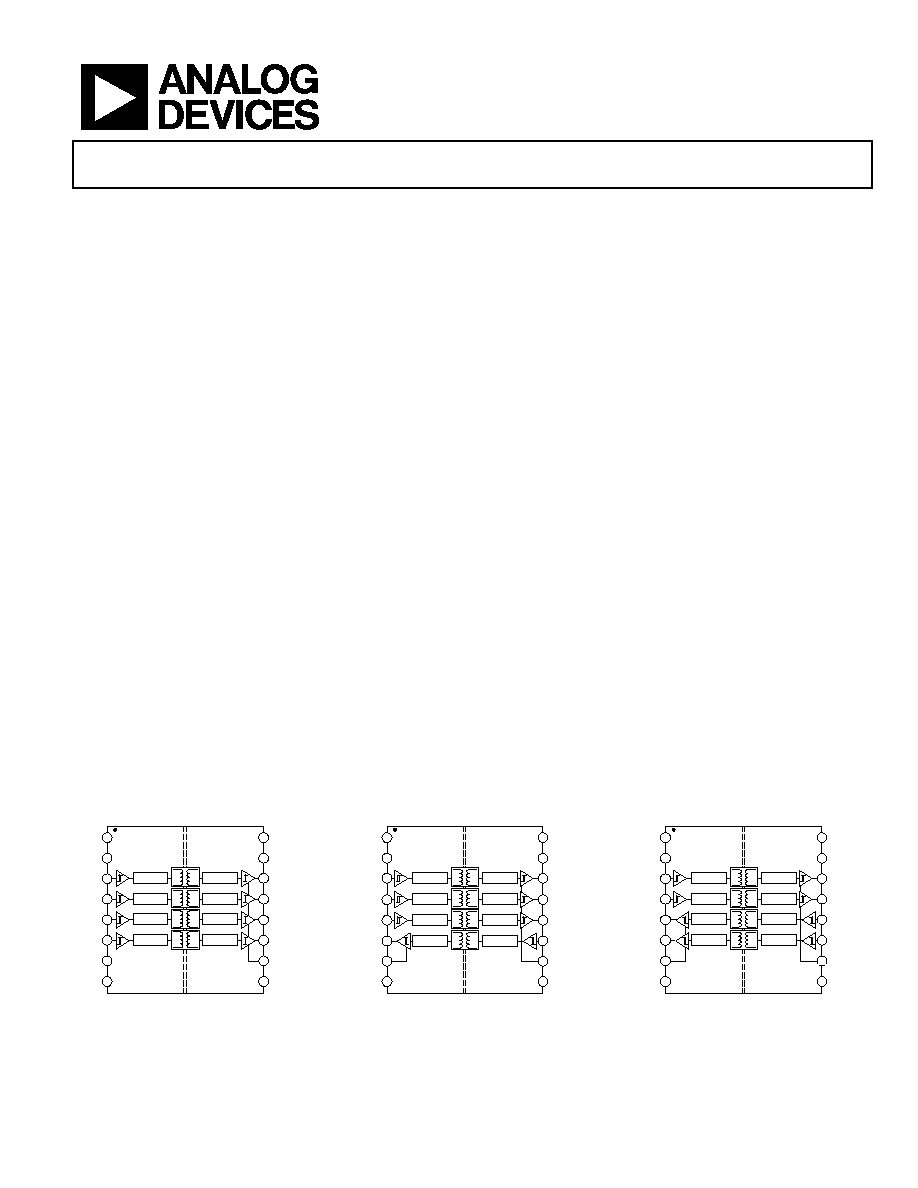
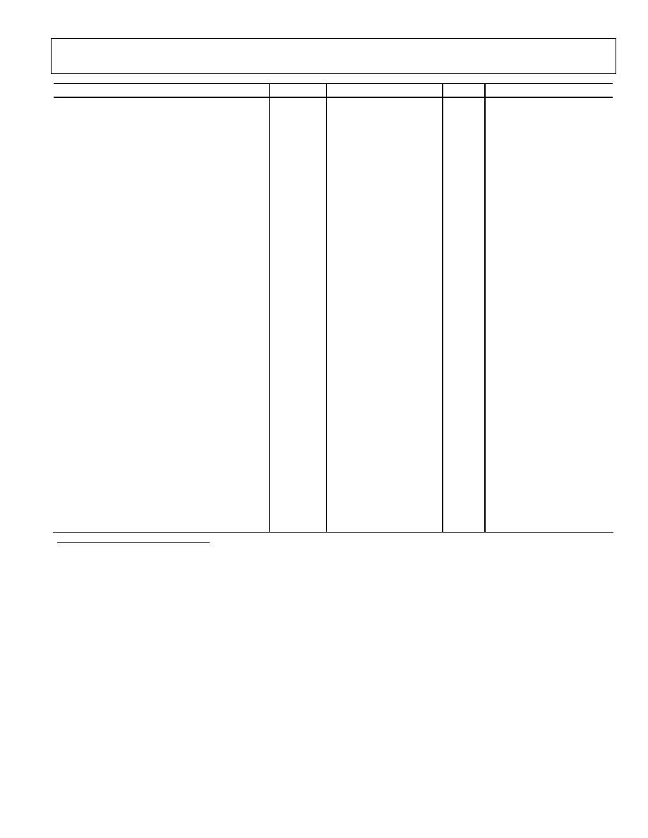
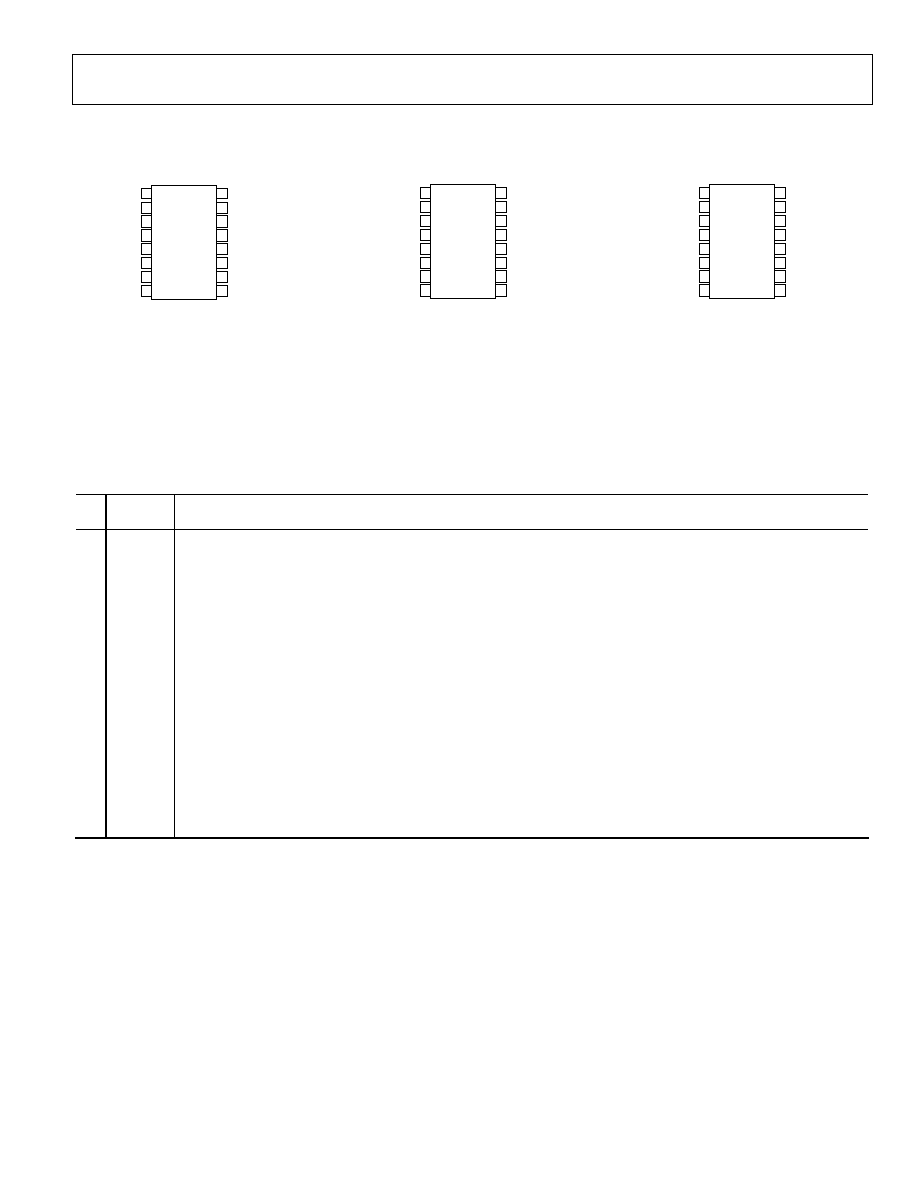
FUNCTIONAL BLOCK DIAGRAMS
ENCODE
DECODE
ENCODE
DECODE
ENCODE
DECODE
ENCODE
DECODE
V
DD1
GND
1
V
IA
V
IB
V
IC
V
ID
NC
GND
1
V
DD2
GND
2
V
OA
V
OB
V
OC
V
OD
V
E2
GND
2
1
2
3
4
5
6
7
8
16
15
14
13
12
11
10
9
03786-
0-
001
Figure 1. ADuM1400 Functional Block Diagram
DECODE
ENCODE
DECODE
ENCODE
ENCODE
DECODE
ENCODE
DECODE
V
DD1
GND
1
V
IA
V
IB
V
IC
V
OD
V
E1
GND
1
V
DD2
GND
2
V
OA
V
OB
V
OC
V
ID
V
E2
GND
2
1
2
3
4
5
6
7
8
16
15
14
13
12
11
10
9
03786-
0-
002
Figure 2. ADuM1401 Functional Block Diagram
DECODE
DECODE
ENCODE
ENCODE
ENCODE
DECODE
ENCODE
DECODE
V
DD1
GND
1
V
IA
V
IB
V
OC
V
OD
V
E1
GND
1
V
DD2
GND
2
V
OA
V
OB
V
IC
V
ID
V
E2
GND
2
1
2
3
4
5
6
7
8
16
15
14
13
12
11
10
9
03786-
0-
003
Figure 3. ADuM1402 Functional Block Diagram

ADuM1400/ADuM1401/ADuM1402
Rev. B | Page 2 of 24
TABLE OF CONTENTS
Specifications..................................................................................... 3
Electrical Characteristics--5 V Operation................................ 3
Electrical Characteristics--3 V Operation................................ 6
Electrical Characteristics--Mixed 5 V/3 V or 3 V/5 V
Operation....................................................................................... 8
Package Characteristics ............................................................. 12
Regulatory Information............................................................. 12
Insulation and Safety-Related Specifications.......................... 12
DIN EN 60747-5-2 (VDE 0884 Part 2) Insulation
Characteristics ............................................................................ 13
Recommended Operating Conditions .................................... 13
Absolute Maximum Ratings.......................................................... 14
ESD Caution................................................................................ 14
Pin Configurations and Pin Function Descriptions .................. 15
Typical Performance Characteristics ........................................... 17
Application Information................................................................ 19
PC Board Layout ........................................................................ 19
Propagation Delay-Related Parameters................................... 19
DC Correctness and Magnetic Field Immunity........................... 19
Power Consumption .................................................................. 20
Outline Dimensions ....................................................................... 21
Ordering Guide .......................................................................... 21
REVISION HISTORY
6/04--Data Sheet Changed from Rev. A to Rev. B.
Changes to Format .............................................................Universal
Changes to Features.......................................................................... 1
Changes to Electrical Characteristics--5 V Operation ............... 3
Changes to Electrical Characteristics--3 V Operation ............... 5
Changes to Electrical Characteristics--Mixed 5 V/3 V or
3 V/5 V Operation ............................................................................ 7
Changes to DIN EN 60747-5-2 (VDE 0884 Part 2)
Insulation Characteristics Title..................................................... 11
Changes to the Ordering Guide.................................................... 19
5/04--Data Sheet Changed from Rev. 0 to Rev. A.
Updated Format..................................................................Universal
Changes to the Features ................................................................... 1
Changes to Table 7 and Table 8..................................................... 14
Changes to Table 9.......................................................................... 15
Changes to the DC Correctness and Magnetic Field Immunity
Section.............................................................................................. 20
Changes to the Power Consumption Section ............................. 21
Changes to the Ordering Guide.................................................... 22
9/03--Revision 0: Initial Version.
ADuM1400/ADuM1401/ADuM1402
Rev. B | Page 3 of 24
SPECIFICATIONS
ELECTRICAL CHARACTERISTICS--5 V OPERATION
1
4.5 V V
DD1
5.5 V, 4.5 V V
DD2
5.5 V; all min/max specifications apply over the entire recommended operation range, unless other-
wise noted; all typical specifications are at T
A
= 25°C, V
DD1
= V
DD2
= 5 V.
Table 1.
Parameter Symbol
Min
Typ
Max
Unit
Test
Conditions
DC SPECIFICATIONS
Input Supply Current, per Channel, Quiescent
I
DDI (Q)
0.50
0.53
mA
Output Supply Current, per Channel, Quiescent
I
DDO (Q)
0.19
0.21
mA
ADuM1400, Total Supply Current, Four Channels
2
DC to 2 Mbps
V
DD1
Supply Current
I
DD1 (Q)
2.2
2.8
mA
DC to 1 MHz logic signal freq.
V
DD2
Supply Current
I
DD2 (Q)
0.9
1.4
mA
DC to 1 MHz logic signal freq.
10 Mbps (BRW and CRW Grades Only)
V
DD1
Supply Current
I
DD1 (10)
8.6
10.6 mA
5 MHz logic signal freq.
V
DD2
Supply Current
I
DD2 (10)
2.6
3.5
mA
5 MHz logic signal freq.
90 Mbps (CRW Grade Only)
V
DD1
Supply Current
I
DD1 (90)
76
100
mA
45 MHz logic signal freq.
V
DD2
Supply Current
I
DD2 (90)
21
25
mA
45 MHz logic signal freq.
ADuM1401, Total Supply Current, Four Channels
2
DC to 2 Mbps
V
DD1
Supply Current
I
DD1 (Q)
1.8
2.4
mA
DC to 1 MHz logic signal freq.
V
DD2
Supply Current
I
DD2 (Q)
1.2
1.8
mA
DC to 1 MHz logic signal freq.
10 Mbps (BRW and CRW Grades Only)
V
DD1
Supply Current
I
DD1 (10)
7.1
9.0
mA
5 MHz logic signal freq.
V
DD2
Supply Current
I
DD2 (10)
4.1
5.0
mA
5 MHz logic signal freq.
90 Mbps (CRW Grade Only)
V
DD1
Supply Current
I
DD1 (90)
62
82
mA
45 MHz logic signal freq.
V
DD2
Supply Current
I
DD2 (90)
35
43
mA
45 MHz logic signal freq.
ADuM1402, Total Supply Current, Four Channels
2
DC to 2 Mbps
V
DD1
or V
DD2
Supply Current
I
DD1 (Q)
, I
DD2 (Q)
1.5
2.1
mA
DC to 1 MHz logic signal freq.
10 Mbps (BRW and CRW Grades Only)
V
DD1
or V
DD2
Supply Current
I
DD1 (10)
, I
DD2 (10)
5.6
7.0
mA
5 MHz logic signal freq.
90 Mbps (CRW Grade Only)
V
DD1
or V
DD2
Supply Current
I
DD1 (90)
, I
DD2 (90)
49
62
mA
45 MHz logic signal freq.
For All Models
Input Currents
I
IA
, I
IB
, I
IC
,
I
ID
, I
E1
, I
E2
10 +0.01 +10
µA 0 V
IA
, V
IB
, V
IC
, V
ID
V
DD1
or V
DD2
,
0 V
E1
, V
E2
V
DD1
or V
DD2
Logic High Input Threshold
V
IH
, V
EH
2.0
V
Logic Low Input Threshold
V
IL
, V
EL
0.8
V
V
DD1
,
V
DD2
0.1
5.0
V
I
Ox
= 20 µA, V
Ix
= V
IxH
Logic High Output Voltages
V
OAH
, V
OBH
,
V
OCH
, V
ODH
V
DD1
,
V
DD2
0.4
4.8
V
I
Ox
= 4 mA, V
Ix
= V
IxH
0.0
0.1
V
I
Ox
= 20 µA, V
Ix
= V
IxL
0.04
0.1
V
I
Ox
= 400 µA, V
Ix
= V
IxL
Logic Low Output Voltages
V
OAL
, V
OBL
,
V
OCL
, V
ODL
0.2
0.4
V
I
Ox
= 4 mA, V
Ix
= V
IxL
ADuM1400/ADuM1401/ADuM1402
Rev. B | Page 4 of 24
Parameter Symbol
Min
Typ
Max
Unit
Test
Conditions
SWITCHING SPECIFICATIONS
ADuM140xARW
Minimum Pulse Width
3
PW
1000 ns
C
L
= 15 pF, CMOS signal levels
Maximum Data Rate
4
1
Mbps
C
L
= 15 pF, CMOS signal levels
Propagation Delay
5
t
PHL
, t
PLH
50 65
100
ns C
L
= 15 pF, CMOS signal levels
Pulse-Width Distortion, |t
PLH
t
PHL
|
5
PWD
40
ns
C
L
= 15 pF, CMOS signal levels
Propagation Delay Skew
6
t
PSK
50
ns
C
L
= 15 pF, CMOS signal levels
Channel-to-Channel Matching
7
t
PSKCD/OD
50
ns
C
L
= 15 pF, CMOS signal levels
ADuM140xBRW
Minimum Pulse Width
3
PW
100
ns
C
L
= 15 pF, CMOS signal levels
Maximum Data Rate
4
10
Mbps
C
L
= 15 pF, CMOS signal levels
Propagation Delay
5
t
PHL
, t
PLH
20 32
50
ns C
L
= 15 pF, CMOS signal levels
Pulse-Width Distortion, |t
PLH
t
PHL
|
5
PWD
3
ns
C
L
= 15 pF, CMOS signal levels
Change vs. Temperature
5
ps/°C
C
L
= 15 pF, CMOS signal levels
Propagation Delay Skew
6
t
PSK
15
ns
C
L
= 15 pF, CMOS signal levels
Channel-to-Channel Matching,
Codirectional Channels
7
t
PSKCD
3
ns
C
L
= 15 pF, CMOS signal levels
Channel-to-Channel Matching,
Opposing-Directional Channels
7
t
PSKOD
6
ns
C
L
= 15 pF, CMOS signal levels
ADuM140xCRW
Minimum Pulse Width
3
PW
8.3
11.1
ns
C
L
= 15 pF, CMOS signal levels
Maximum Data Rate
4
90
120
Mbps
C
L
= 15 pF, CMOS signal levels
Propagation Delay
5
t
PHL
, t
PLH
18 27
32
ns C
L
= 15 pF, CMOS signal levels
Pulse-Width Distortion, |t
PLH
t
PHL
|
5
PWD 0.5
2
ns
C
L
= 15 pF, CMOS signal levels
Change vs. Temperature
3
ps/°C
C
L
= 15 pF, CMOS signal levels
Propagation Delay Skew
6
t
PSK
10
ns
C
L
= 15 pF, CMOS signal levels
Channel-to-Channel Matching,
Codirectional Channels
7
t
PSKCD
2
ns
C
L
= 15 pF, CMOS signal levels
Channel-to-Channel Matching,
Opposing-Directional Channels
7
t
PSKOD
5
ns
C
L
= 15 pF, CMOS signal levels
For All Models
Output Disable Propagation Delay
(High/Low-to-High Impedance)
t
PHZ
, t
PLH
6
8
ns
C
L
= 15 pF, CMOS signal levels
Output Enable Propagation Delay
(High Impedance to High/Low)
t
PZH
, t
PZL
6
8
ns
C
L
= 15 pF, CMOS signal levels
Output Rise/Fall Time (10% to 90%)
t
R
/t
F
2.5
ns
C
L
= 15 pF, CMOS signal levels
Common-Mode Transient Immunity
at Logic High Output
8
|CM
H
| 25 35
kV/µs
V
Ix
= V
DD1
/V
DD2
, V
CM
= 1000 V,
transient magnitude = 800 V
Common-Mode Transient Immunity
at Logic Low Output
8
|CM
L
| 25 35
kV/µs
V
Ix
= 0 V, V
CM
= 1000 V,
transient magnitude = 800 V
Refresh Rate
f
r
1.2
Mbps
Input Dynamic Supply Current, per Channel
9
I
DDI (D)
0.19
mA/Mbps
Output Dynamic Supply Current, per Channel
9
I
DDO (D)
0.05
mA/Mbps
See Notes on next page.

ADuM1400/ADuM1401/ADuM1402
Rev. B | Page 5 of 24
1
All voltages are relative to their respective ground.
2
The supply current values for all four channels are combined when running at identical data rates. Output supply current values are specified with no output load
present. The supply current associated with an individual channel operating at a given data rate may be calculated as described in the Power Consumption section on
Page 20. See
through
for information on per-channel supply current as a function of data rate for unloaded and loaded conditions. See
through
for total I
Figure 8
Figure 8
Figure 10
Figure 10
Figure 11
Figure 14
DD1
and I
DD2
supply currents as a function of data rate for ADuM1400/ADuM1401/ADuM1402 channel configurations.
3
The minimum pulse width is the shortest pulse width at which the specified pulse-width distortion is guaranteed.
4
The maximum data rate is the fastest data rate at which the specified pulse-width distortion is guaranteed.
5
t
PHL
propagation delay is measured from the 50% level of the falling edge of the V
Ix
signal to the 50% level of the falling edge of the V
Ox
signal. t
PLH
propagation delay is
measured from the 50% level of the rising edge of the V
Ix
signal to the 50% level of the rising edge of the V
Ox
signal.
6
t
PSK
is the magnitude of the worst-case difference in t
PHL
or t
PLH
that is measured between units at the same operating temperature, supply voltages, and output load
within the recommended operating conditions.
7
Codirectional channel-to-channel matching is the absolute value of the difference in propagation delays between any two channels with inputs on the same side of
the isolation barrier. Opposing-directional channel-to-channel matching is the absolute value of the difference in propagation delays between any two channels with
inputs on opposing sides of the isolation barrier.
8
CM
H
is the maximum common-mode voltage slew rate that can be sustained while maintaining V
O
> 0.8 V
DD2
. CM
L
is the maximum common-mode voltage slew rate
that can be sustained while maintaining V
O
< 0.8 V. The common-mode voltage slew rates apply to both rising and falling common-mode voltage edges. The transient
magnitude is the range over which the common mode is slewed.
9
Dynamic supply current is the incremental amount of supply current required for a 1 Mbps increase in signal data rate. See
through
for information
on per-channel supply current for unloaded and loaded conditions. See the
section on Page 20 for guidance on calculating the per-channel sup-
ply current for a given data rate.
Power Consumption
ADuM1400/ADuM1401/ADuM1402
Rev. B | Page 6 of 24
ELECTRICAL CHARACTERISTICS--3 V OPERATION
1
2.7 V V
DD1
3.6 V, 2.7 V V
DD2
3.6 V; all min/max specifications apply over the entire recommended operation range, unless other-
wise noted; all typical specifications are at T
A
= 25°C, V
DD1
= V
DD2
= 3.0 V.
Table 2.
Parameter Symbol
Min
Typ
Max Unit
Test
Conditions
DC SPECIFICATIONS
Input Supply Current, per Channel, Quiescent
I
DDI (Q)
0.26
0.31
mA
Output Supply Current, per Channel, Quiescent
I
DDO (Q)
0.11
0.14
mA
ADuM1400, Total Supply Current, Four Channels
2
DC to 2 Mbps
V
DD1
Supply Current
I
DD1 (Q)
1.2
1.9
mA
DC to 1 MHz logic signal freq.
V
DD2
Supply Current
I
DD2 (Q)
0.5
0.9
mA
DC to 1 MHz logic signal freq.
10 Mbps (BRW and CRW Grades Only)
V
DD1
Supply Current
I
DD1 (10)
4.5
6.5
mA
5 MHz logic signal freq.
V
DD2
Supply Current
I
DD2 (10)
1.4
2.0
mA
5 MHz logic signal freq.
90 Mbps (CRW Grade Only)
V
DD1
Supply Current
I
DD1 (90)
42
65
mA
45 MHz logic signal freq.
V
DD2
Supply Current
I
DD2 (90)
11
15
mA
45 MHz logic signal freq.
ADuM1401, Total Supply Current, Four Channels
2
DC to 2 Mbps
V
DD1
Supply Current
I
DD1 (Q)
1.0
1.6
mA
DC to 1 MHz logic signal freq.
V
DD2
Supply Current
I
DD2 (Q)
0.7
1.2
mA
DC to 1 MHz logic signal freq.
10 Mbps (BRW and CRW Grades Only)
V
DD1
Supply Current
I
DD1 (10)
3.7
5.4
mA
5 MHz logic signal freq.
V
DD2
Supply Current
I
DD2 (10)
2.2
3.0
mA
5 MHz logic signal freq.
90 Mbps (CRW Grade Only)
V
DD1
Supply Current
I
DD1 (90)
34
52
mA
45 MHz logic signal freq.
V
DD2
Supply Current
I
DD2 (90)
19
27
mA
45 MHz logic signal freq.
ADuM1402, Total Supply Current, Four Channels
2
DC to 2 Mbps
V
DD1
or V
DD2
Supply Current
I
DD1 (Q)
, I
DD2 (Q)
0.9
1.5
mA
DC to 1 MHz logic signal freq.
10 Mbps (BRW and CRW Grades Only)
V
DD1
or V
DD2
Supply Current
I
DD1 (10)
, I
DD2 (10)
3.0
4.2
mA
5 MHz logic signal freq.
90 Mbps (CRW Grade Only)
V
DD1
or V
DD2
Supply Current
I
DD1 (90)
, I
DD2 (90)
27
39
mA
45 MHz logic signal freq.
For All Models
Input Currents
I
IA
, I
IB
, I
IC,
I
ID
, I
E1
, I
E2
10 +0.01 +10
µA
0 V
IA
, V
IB
, V
IC
, V
ID
V
DD1
or
V
DD2
, 0 V
E1
,V
E2
V
DD1
or V
DD2
Logic High Input Threshold
V
IH
, V
EH
1.6
V
Logic Low Input Threshold
V
IL
, V
EL
0.4
V
V
DD1
, V
DD2
0.1 3.0
V
I
Ox
= 20 µA, V
Ix
= V
IxH
Logic High Output Voltages
V
OAH
, V
OBH
,
V
OCH
, V
ODH
V
DD1
, V
DD2
0.4 2.8
V
I
Ox
= 4 mA, V
Ix
= V
IxH
0.0
0.1
V
I
Ox
= 20 µA, V
Ix
= V
IxL
0.04
0.1
V
I
Ox
= 400 µA, V
Ix
= V
IxL
Logic Low Output Voltages
V
OAL
, V
OBL
,
V
OCL
, V
ODL
0.2
0.4
V
I
Ox
= 4 mA, V
Ix
= V
IxL
SWITCHING SPECIFICATIONS
ADuM140xARW
Minimum Pulse Width
3
PW
1000 ns
C
L
= 15 pF, CMOS signal levels
Maximum Data Rate
4
1
Mbps
C
L
= 15 pF, CMOS signal levels
Propagation Delay
5
t
PHL
, t
PLH
50 75
100
ns
C
L
= 15 pF, CMOS signal levels
Pulse-Width Distortion, |t
PLH
t
PHL
|
5
PWD
40
ns C
L
= 15 pF, CMOS signal levels
Propagation Delay Skew
6
t
PSK
50
ns
C
L
= 15 pF, CMOS signal levels
Channel-to-Channel Matching
7
t
PSKCD/OD
50
ns
C
L
= 15 pF, CMOS signal levels
ADuM1400/ADuM1401/ADuM1402
Rev. B | Page 7 of 24
Parameter Symbol
Min
Typ
Max Unit
Test
Conditions
ADuM140xBRW
Minimum Pulse Width
3
PW
100
ns
C
L
= 15 pF, CMOS signal levels
Maximum Data Rate
4
10
Mbps
C
L
= 15 pF, CMOS signal levels
Propagation Delay
5
t
PHL
, t
PLH
20 38
50
ns
C
L
= 15 pF, CMOS signal levels
Pulse-Width Distortion, |t
PLH
t
PHL
|
5
PWD
3
ns C
L
= 15 pF, CMOS signal levels
Change vs. Temperature
5
ps/°C
C
L
= 15 pF, CMOS signal levels
Propagation Delay Skew
6
t
PSK
22
ns
C
L
= 15 pF, CMOS signal levels
Channel-to-Channel Matching,
Codirectional Channels
7
t
PSKCD
3
ns
C
L
= 15 pF, CMOS signal levels
Channel-to-Channel Matching,
Opposing-Directional Channels
7
t
PSKOD
6
ns
C
L
= 15 pF, CMOS signal levels
ADuM140xCRW
Minimum Pulse Width
3
PW
8.3
11.1
ns
C
L
= 15 pF, CMOS signal levels
Maximum Data Rate
4
90
120
Mbps
C
L
= 15 pF, CMOS signal levels
Propagation Delay
5
t
PHL
, t
PLH
20 34
45
ns
C
L
= 15 pF, CMOS signal levels
Pulse-Width Distortion, |t
PLH
t
PHL
|
5
PWD
0.5
2
ns C
L
= 15 pF, CMOS signal levels
Change vs. Temperature
3
ps/°C
C
L
= 15 pF, CMOS signal levels
Propagation Delay Skew
6
t
PSK
16
ns
C
L
= 15 pF, CMOS signal levels
Channel-to-Channel Matching,
Codirectional Channels
7
t
PSKCD
2
ns
C
L
= 15 pF, CMOS signal levels
Channel-to-Channel Matching,
Opposing-Directional Channels
7
t
PSKOD
5
ns
C
L
= 15 pF, CMOS signal levels
For All Models
Output Disable Propagation Delay
(High/Low-to-High Impedance)
t
PHZ
, t
PLH
6
8
ns
C
L
= 15 pF, CMOS signal levels
Output Enable Propagation Delay
(High Impedance to High/Low)
t
PZH
, t
PZL
6
8
ns
C
L
= 15 pF, CMOS signal levels
Output Rise/Fall Time (10% to 90%)
t
R
/t
F
3
ns
C
L
= 15 pF, CMOS signal levels
Common-Mode Transient Immunity
at Logic High Output
8
|CM
H
| 25
35
kV/µs
V
Ix
= V
DD1
/V
DD2
, V
CM
= 1000 V,
transient magnitude = 800 V
Common-Mode Transient Immunity
at Logic Low Output
8
|CM
L
| 25
35
kV/µs
V
Ix
= 0 V, V
CM
= 1000 V,
transient magnitude = 800 V
Refresh Rate
f
r
1.1
Mbps
Input Dynamic Supply Current, per Channel
9
I
DDI (D)
0.10
mA/Mbps
Output Dynamic Supply Current, per Channel
9
I
DDO (D)
0.03
mA/Mbps
1
All voltages are relative to their respective ground.
2
The supply current values for all four channels are combined when running at identical data rates. Output supply current values are specified with no output load
present. The supply current associated with an individual channel operating at a given data rate may be calculated as described in the Power Consumption section on
Page 20. See
through
for information on per-channel supply current as a function of data rate for unloaded and loaded conditions. See
through
for total I
Figure 8
Figure 8
Figure 10
Figure 10
Figure 11
Figure 14
DD1
and I
DD2
supply currents as a function of data rate for ADuM1400/ADuM1401/ADuM1402 channel configurations.
3
The minimum pulse width is the shortest pulse width at which the specified pulse-width distortion is guaranteed.
4
The maximum data rate is the fastest data rate at which the specified pulse-width distortion is guaranteed.
5
t
PHL
propagation delay is measured from the 50% level of the falling edge of the V
Ix
signal to the 50% level of the falling edge of the V
Ox
signal. t
PLH
propagation delay is
measured from the 50% level of the rising edge of the V
Ix
signal to the 50% level of the rising edge of the V
Ox
signal.
6
t
PSK
is the magnitude of the worst-case difference in t
PHL
or t
PLH
that is measured between units at the same operating temperature, supply voltages, and output load
within the recommended operating conditions.
7
Codirectional channel-to-channel matching is the absolute value of the difference in propagation delays between any two channels with inputs on the same side of
the isolation barrier. Opposing-directional channel-to-channel matching is the absolute value of the difference in propagation delays between any two channels with
inputs on opposing sides of the isolation barrier.
8
CM
H
is the maximum common-mode voltage slew rate that can be sustained while maintaining V
O
> 0.8 V
DD2
. CM
L
is the maximum common-mode voltage slew rate
that can be sustained while maintaining V
O
< 0.8 V. The common-mode voltage slew rates apply to both rising and falling common-mode voltage edges. The transient
magnitude is the range over which the common mode is slewed.
9
Dynamic supply current is the incremental amount of supply current required for a 1 Mbps increase in signal data rate. See
through
for information
on per-channel supply current for unloaded and loaded conditions. See the
section on Page 20 for guidance on calculating the per-channel sup-
ply current for a given data rate.
Power Consumption

ADuM1400/ADuM1401/ADuM1402
Rev. B | Page 8 of 24
ELECTRICAL CHARACTERISTICS--MIXED 5 V/3 V OR 3 V/5 V OPERATION
1
5 V/3 V operation: 4.5 V V
DD1
5.5 V, 2.7 V V
DD2
3.6 V; 3 V/5 V operation: 2.7 V V
DD1
3.6 V, 4.5 V V
DD2
5.5 V; all min/max
specifications apply over the entire recommended operation range, unless otherwise noted; all typical specifications are at
T
A
= 25°C; V
DD1
= 3.0 V, V
DD2
= 5 V; or V
DD1
= 5 V, V
DD2
= 3.0 V.
Table 3.
Parameter Symbol
Min
Typ
Max Unit
Test
Conditions
DC SPECIFICATIONS
Input Supply Current, per Channel, Quiescent I
DDI (Q)
5 V/3 V Operation
0.50
0.53 mA
3 V/5 V Operation
0.26
0.31 mA
Output Supply Current, per Channel, Quiescent
I
DDO (Q)
5 V/3 V Operation
0.11
0.14 mA
3 V/5 V Operation
0.19
0.21 mA
ADuM1400, Total Supply Current, Four Channels
2
DC to 2 Mbps
V
DD1
Supply Current
I
DD1 (Q)
5 V/3 V Operation
2.2
2.8
mA
DC to 1 MHz logic signal freq.
3 V/5 V Operation
1.2
1.9
mA
DC to 1 MHz logic signal freq.
V
DD2
Supply Current
I
DD2 (Q)
5 V/3 V Operation
0.5
0.9
mA
DC to 1 MHz logic signal freq.
3 V/5 V Operation
0.9
1.4
mA
DC to 1 MHz logic signal freq.
10 Mbps (BRW and CRW Grades Only)
V
DD1
Supply Current
I
DD1 (10)
5 V/3 V Operation
8.6
10.6 mA
5 MHz logic signal freq.
3 V/5 V Operation
4.5
6.5
mA
5 MHz logic signal freq.
V
DD2
Supply Current
I
DD2 (10)
5 V/3 V Operation
1.4
2.0
mA
5 MHz logic signal freq.
3 V/5 V Operation
2.6
3.5
mA
5 MHz logic signal freq.
90 Mbps (CRW Grade Only)
V
DD1
Supply Current
I
DD1 (90)
5 V/3 V Operation
76
100
mA
45 MHz logic signal freq.
3 V/5 V Operation
42
65
mA
45 MHz logic signal freq.
V
DD2
Supply Current
I
DD2 (90)
5 V/3 V Operation
11
15
mA
45 MHz logic signal freq.
3 V/5 V Operation
21
25
mA
45 MHz logic signal freq.
ADuM1401, Total Supply Current, Four Channels
2
DC to 2 Mbps
V
DD1
Supply Current
I
DD1 (Q)
5 V/3 V Operation
1.8
2.4
mA
DC to 1 MHz logic signal freq.
3 V/5 V Operation
1.0
1.6
mA
DC to 1 MHz logic signal freq.
V
DD2
Supply Current
I
DD2 (Q)
5 V/3 V Operation
0.7
1.2
mA
DC to 1 MHz logic signal freq.
3 V/5 V Operation
1.2
1.8
mA
DC to 1 MHz logic signal freq.
10 Mbps (BRW and CRW Grades Only)
V
DD1
Supply Current
I
DD1 (10)
5 V/3 V Operation
7.1
9.0
mA
5 MHz logic signal freq.
3 V/5 V Operation
3.7
5.4
mA
5 MHz logic signal freq.
V
DD2
Supply Current
I
DD2 (10)
5 V/3 V Operation
2.2
3.0
mA
5 MHz logic signal freq.
3 V/5 V Operation
4.1
5.0
mA
5 MHz logic signal freq.
ADuM1400/ADuM1401/ADuM1402
Rev. B | Page 9 of 24
Parameter Symbol
Min
Typ
Max Unit
Test
Conditions
90 Mbps (CRW Grade Only)
V
DD1
Supply Current
I
DD1 (90)
5 V/3 V Operation
62
82
mA
45 MHz logic signal freq.
3 V/5 V Operation
34
52
mA
45 MHz logic signal freq.
V
DD2
Supply Current
I
DD2 (90)
5 V/3 V Operation
19
27
mA
45 MHz logic signal freq.
3 V/5 V Operation
35
43
mA
45 MHz logic signal freq.
ADuM1402, Total Supply Current, Four Channels
2
DC to 2 Mbps
V
DD1
Supply Current
I
DD1 (Q)
5 V/3 V Operation
1.5
2.1
mA
DC to 1 MHz logic signal freq.
3 V/5 V Operation
0.9
1.5
mA
DC to 1 MHz logic signal freq.
V
DD2
Supply Current
I
DD2 (Q)
5 V/3 V Operation
0.9
1.5
mA
DC to 1 MHz logic signal freq.
3 V/5 V Operation
1.5
2.1
mA
DC to 1 MHz logic signal freq.
10 Mbps (BRW and CRW Grades Only)
V
DD1
Supply Current
I
DD1 (10)
5 V/3 V Operation
5.6
7.0
mA
5 MHz logic signal freq.
3 V/5 V Operation
3.0
4.2
mA
5 MHz logic signal freq.
V
DD2
Supply Current
I
DD2 (10)
5 V/3 V Operation
3.0
4.2
mA
5 MHz logic signal freq.
3 V/5 V Operation
5.6
7.0
mA
5 MHz logic signal freq.
90 Mbps (CRW Grade Only)
V
DD1
Supply Current
I
DD1 (90)
5 V/3 V Operation
49
62
mA
45 MHz logic signal freq.
3 V/5 V Operation
27
39
mA
45 MHz logic signal freq.
V
DD2
Supply Current
I
DD2 (90)
5 V/3 V Operation
27
39
mA
45 MHz logic signal freq.
3 V/5 V Operation
49
62
mA
45 MHz logic signal freq.
For All Models
Input Currents
I
IA
, I
IB
, I
IC
,
I
ID
, I
E1
, I
E2
10 +0.01
+10
µA
0 V
IA
,V
IB
, V
IC
,V
ID
V
DD1
or
V
DD2
, 0 V
E1
,V
E2
V
DD1
or V
DD2
Logic High Input Threshold
V
IH
, V
EH
5 V/3 V Operation
2.0
V
3 V/5 V Operation
1.6
V
Logic Low Input Threshold
V
IL
, V
EL
5 V/3 V Operation
0.8
V
3 V/5 V Operation
0.4
V
V
DD1
/
V
DD2
0.1
V
DD1/
V
DD2
V
I
Ox
= 20 µA, V
Ix
= V
IxH
Logic High Output Voltages
V
OAH
, V
OBH
,
V
OCH
, V
ODH
V
DD1
/
V
DD2
0.4
V
DD1
/
V
DD2
0.2
V
I
Ox
= 4 mA, V
Ix
= V
IxH
0.0
0.1
V
I
Ox
= 20 µA, V
Ix
= V
IxL
0.04
0.1
V
I
Ox
= 400 µA, V
Ix
= V
IxL
Logic Low Output Voltages
V
OAL,
V
OBL,
V
OCL
, V
ODL
0.2
0.4
V
I
Ox
= 4 mA, V
Ix
= V
IxL
SWITCHING SPECIFICATIONS
ADuM140xARW
Minimum Pulse Width
3
PW
1000 ns
C
L
= 15 pF, CMOS signal levels
Maximum Data Rate
4
1
Mbps
C
L
= 15 pF, CMOS signal levels
Propagation Delay
5
t
PHL
, t
PLH
50 70 100
ns
C
L
= 15 pF, CMOS signal levels
Pulse-Width Distortion, |t
PLH
t
PHL
|
5
PWD
40
ns
C
L
= 15 pF, CMOS signal levels
Propagation Delay Skew
6
t
PSK
50
ns
C
L
= 15 pF, CMOS signal levels
Channel-to-Channel Matching
7
t
PSKCD/OD
50
ns
C
L
= 15 pF, CMOS signal levels

ADuM1400/ADuM1401/ADuM1402
Rev. B | Page 10 of 24
Parameter Symbol
Min
Typ
Max Unit
Test
Conditions
ADuM140xBRW
Minimum Pulse Width
3
PW
100
ns
C
L
= 15 pF,CMOS signal levels
Maximum Data Rate
4
10
Mbps
C
L
= 15 pF, CMOS signal levels
Propagation Delay
5
t
PHL
, t
PLH
15 35 50
ns
C
L
= 15 pF, CMOS signal levels
Pulse-Width Distortion, |t
PLH
t
PHL
|
5
PWD
3
ns
C
L
= 15 pF, CMOS signal levels
Change vs. Temperature
5
ps/°C
C
L
= 15 pF, CMOS signal levels
Propagation Delay Skew
6
t
PSK
22
ns
C
L
= 15 pF, CMOS signal levels
Channel-to-Channel Matching,
Codirectional Channels
7
t
PSKCD
3
ns
C
L
= 15 pF, CMOS signal levels
Channel-to-Channel Matching,
Opposing-Directional Channels
7
t
PSKOD
6
ns
C
L
= 15 pF, CMOS signal levels
ADuM140xCRW
Minimum Pulse Width
3
PW
8.3
11.1
ns
Maximum Data Rate
4
90
120
Mbps
C
L
= 15 pF, CMOS signal levels
C
L
= 15 pF, CMOS signal levels
Propagation Delay
5
t
PHL
, t
PLH
20 30 40
ns
C
L
= 15 pF, CMOS signal levels
Pulse-Width Distortion, |t
PLH
t
PHL
|
5
PWD
0.5 2
ns
C
L
= 15 pF, CMOS signal levels
Change vs. Temperature
3
ps/°C
C
L
= 15 pF, CMOS signal levels
Propagation Delay Skew
6
t
PSK
14
ns
C
L
= 15 pF, CMOS signal levels
Channel-to-Channel Matching,
Codirectional Channels
7
t
PSKCD
2
ns
C
L
= 15 pF, CMOS signal levels
Channel-to-Channel Matching,
Opposing-Directional Channels
7
t
PSKOD
5
ns
C
L
= 15 pF, CMOS signal levels
For All Models
Output Disable Propagation Delay
(High/Low to High Impedance)
t
PHZ
, t
PLH
6 8
ns
C
L
= 15 pF, CMOS signal levels
Output Enable Propagation Delay
(High Impedance to High/Low)
t
PZH
, t
PZL
6 8
ns
C
L
= 15 pF, CMOS signal levels
Output Rise/Fall Time (10% to 90%)
t
R
/t
f
C
L
= 15 pF, CMOS signal levels
5 V/3 V Operation
3.0
ns
3 V/5 V Operation
2.5
ns
Common-Mode Transient Immunity
at Logic High Output
8
|CM
H
| 25 35
kV/µs
V
Ix
= V
DD1
/V
DD2
, V
CM
= 1000 V,
transient magnitude = 800 V
Common-Mode Transient Immunity
at Logic Low Output
8
|CM
L
| 25 35
kV/µs
V
Ix
= 0 V, V
CM
= 1000 V,
transient magnitude = 800 V
Refresh Rate
f
r
5 V/3 V Operation
1.2
Mbps
3 V/5 V Operation
1.1
Mbps
Input Dynamic Supply Current, per Channel
9
I
DDI (D)
5 V/3 V Operation
0.19
mA/Mbps
3 V/5 V Operation
0.10
mA/Mbps
Output Dynamic Supply Current, per Channel
9
I
DDI (D)
5 V/3 V Operation
0.03
mA/Mbps
3 V/5 V Operation
0.05
mA/Mbps
See Notes on next page.

ADuM1400/ADuM1401/ADuM1402
Rev. B | Page 11 of 24
1
All voltages are relative to their respective ground.
2
The supply current values for all four channels are combined when running at identical data rates. Output supply current values are specified with no output load present. The
supply current associated with an individual channel operating at a given data rate may be calculated as described in the Power Consumption section on Page 20. See Figure 8
through Figure 10 for information on per-channel supply current as a function of data rate for unloaded and loaded conditions. See Figure 11 through Figure 14 for total I
DD1
and
I
DD2
supply currents as a function of data rate for ADuM1400/ADuM1401/ADuM1402 channel configurations.
3
The minimum pulse width is the shortest pulse width at which the specified pulse-width distortion is guaranteed.
4
The maximum data rate is the fastest data rate at which the specified pulse-width distortion is guaranteed.
5
t
PHL
propagation delay is measured from the 50% level of the falling edge of the V
Ix
signal to the 50% level of the falling edge of the V
Ox
signal. t
PLH
propagation delay is measured
from the 50% level of the rising edge of the V
Ix
signal to the 50% level of the rising edge of the V
Ox
signal.
6
t
PSK
is the magnitude of the worst-case difference in t
PHL
or t
PLH
that is measured between units at the same operating temperature, supply voltages, and output load within the
recommended operating conditions.
7
Codirectional channel-to-channel matching is the absolute value of the difference in propagation delays between any two channels with inputs on the same side of the isolation
barrier. Opposing-directional channel-to-channel matching is the absolute value of the difference in propagation delays between any two channels with inputs on opposing sides
of the isolation barrier.
8
CM
H
is the maximum common-mode voltage slew rate that can be sustained while maintaining V
O
> 0.8 V
DD2
. CM
L
is the maximum common-mode voltage slew rate that can be
sustained while maintaining V
O
< 0.8 V. The common-mode voltage slew rates apply to both rising and falling common-mode voltage edges. The transient magnitude is the range
over which the common mode is slewed.
9
Dynamic supply current is the incremental amount of supply current required for a 1 Mbps increase in signal data rate. See Figure 8 through Figure 10 for information on per-
channel supply current for unloaded and loaded conditions. See the Power Consumption section on Page 20 for guidance on calculating the per-channel supply current for a
given data rate.

ADuM1400/ADuM1401/ADuM1402
Rev. B | Page 12 of 24
PACKAGE CHARACTERISTICS
Table 4.
Parameter Symbol
Min
Typ
Max
Unit
Test
Conditions
Resistance (Input-Output)
1
R
I-O
10
12
Capacitance (Input-Output)
1
C
I-O
2.2
pF
f = 1 MHz
Input Capacitance
2
C
I
4.0
pF
IC Junction-to-Case Thermal Resistance, Side 1
JCI
33
°C/W
IC Junction-to-Case Thermal Resistance, Side 2
JCO
28
°C/W
Thermocouple located
at center of package
underside
1
Device considered a 2-terminal device; Pins 1, 2, 3, 4, 5, 6, 7, and 8 shorted together and Pins 9, 10, 11, 12, 13, 14, 15, and 16 shorted together.
2
Input capacitance is from any input data pin to ground.
REGULATORY INFORMATION
The ADuM140x have been approved by the organizations listed in Table 5.
Table 5.
UL
1
CSA VDE
2
Recognized under 1577
component recognition program
1
Double insulation, 2500 V rms
isolation voltage
File E214100
Approved under CSA Component
Acceptance Notice #5A
Reinforced insulation per
CSA 60950-1-03 and IEC 60950-1,
400 V rms maximum working voltage
File 205078
Certified according to DIN EN 60747-5-2
(VDE 0884 Part 2): 2003-01
2
Basic insulation, 560 V peak
Complies with DIN EN 60747-5-2 (VDE 0884 Part 2): 2003-
01, DIN EN 60950 (VDE 0805): 2001-12; EN 60950:2000
Reinforced insulation, 560 V peak
File 2471900-4880-0001
1
In accordance with UL1577, each ADuM140x is proof tested by applying an insulation test voltage 3000 V rms for 1 second (current leakage detection limit = 5 µA).
2
In accordance with DIN EN 60747-5-2, each ADuM140x is proof tested by applying an insulation test voltage 1050 V peak for 1 second (partial discharge detection
limit = 5 pC). A "*" mark branded on the component designates DIN EN 60747-5-2 approval.
INSULATION AND SAFETY-RELATED SPECIFICATIONS
Table 6.
Parameter Symbol
Value
Unit
Conditions
Rated Dielectric Insulation Voltage
2500
V rms
1 minute duration
Minimum External Air Gap (Clearance)
L(I01)
8.40 min
mm
Measured from input terminals to output terminals,
shortest distance through air
Minimum External Tracking (Creepage)
L(I02)
8.10 min
mm
Measured from input terminals to output terminals,
shortest distance path along body
Minimum Internal Gap (Internal Clearance)
0.017 min mm
Insulation distance through insulation
Tracking Resistance (Comparative Tracking Index) CTI
>175
V
DIN IEC 112/VDE 0303 Part 1
Isolation Group
IIIa
Material Group (DIN VDE 0110, 1/89, Table 1)
ADuM1400/ADuM1401/ADuM1402
Rev. B | Page 13 of 24
DIN EN 60747-5-2 (VDE 0884 PART 2) INSULATION CHARACTERISTICS
Table 7.
Description Symbol
Characteristic
Unit
Installation Classification per DIN VDE 0110
For Rated Mains Voltage 150 V rms
For Rated Mains Voltage 300 V rms
For Rated Mains Voltage 400 V rms
IIV
IIII
III
Climatic Classification
40/105/21
Pollution Degree (DIN VDE 0110, Table 1)
2
Maximum Working Insulation Voltage
V
IORM
560 V
peak
Input to Output Test Voltage, Method b1
V
IORM
× 1.875 = V
PR
, 100% Production Test, t
m
= 1 sec, Partial Discharge < 5 pC
V
PR
1050 V
peak
Input to Output Test Voltage, Method a
After Environmental Tests Subgroup 1
V
IORM
× 1.6 = V
PR
, t
m
= 60 sec, Partial Discharge < 5 pC
After Input and/or Safety Test Subgroup 2/3
V
IORM
× 1.2 = V
PR
, t
m
= 60 sec, Partial Discharge < 5 pC
V
PR
896
672
V peak
V peak
Highest Allowable Overvoltage (Transient Overvoltage, t
TR
= 10 sec)
V
TR
4000 V
peak
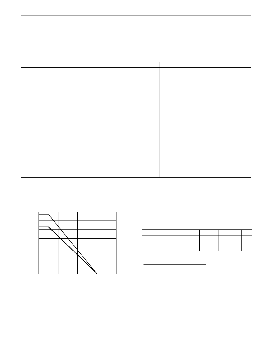
Safety-Limiting Values (Maximum value allowed in the event of a failure; also see
Thermal Derating Curve, Figure 4)
Case Temperature
Side 1 Current
Side 2 Current
T
S
I
S1
I
S2
150
265
335
°C
mA
mA
Insulation Resistance at T
S
, V
IO
= 500 V
R
S
>10
9
This isolator is suitable for basic electrical isolation only within the safety limit data. Maintenance of the safety data is ensured by protec-
tive circuits.
The * marking on packages denotes DIN EN 60747-5-2 approval for 560 V peak working voltage.
CASE TEMPERATURE (°C)
S
A
FE
TY
-LIMITING CURRE
NT (mA)
0
0
350
300
250
200
150
100
50
50
100
150
200
SIDE #1
SIDE #2
03787-0-003
Figure 4. Thermal Derating Curve, Dependence of Safety Limiting Values
with Case Temperature per DIN EN 60747-5-2
RECOMMENDED OPERATING CONDITIONS
Table 8.
Parameter Symbol
Min
Max
Unit
Operating Temperature
T
A
40 +105 °C
Supply Voltages
1
V
DD1
, V
DD 2
2.7 5.5 V
Input Signal Rise and Fall Times
1.0
ms
1
All voltages are relative to their respective ground.
See the DC Correctness and Magnetic Field Immunity section on Page 19 for
information on immunity to external magnetic fields.
ADuM1400/ADuM1401/ADuM1402
Rev. B | Page 14 of 24
ABSOLUTE MAXIMUM RATINGS
Ambient temperature = 25°C, unless otherwise noted.
Table 9.
Parameter Symbol
Min
Max
Unit
Storage Temperature
T
ST
65 +150
°C
Ambient Operating Temperature
T
A
40 +105
°C
Supply Voltages
1
V
DD1
, V
DD2
0.5 +7.0
V
Input Voltage
1, 2
V
IA
, V
IB
, V
IC
, V
ID
, V
E1
,V
E2
0.5 V
DDI
+ 0.5
V
Output Voltage
1, 2
V
OA
, V
OB
, V
OC
, V
OD
0.5 V
DDO
+ 0.5
V
Average Output Current, Per Pin
3
Side 1
I
O1
18 +18
mA
Side 2
I
O2
22 +22
mA
Common-Mode Transients
4
100
+100
kV/µs
1
All voltages are relative to their respective ground.
2
V
DDI
and V
DDO
refer to the supply voltages on the input and output sides of a given channel, respectively. See the
section.
PC Board Layout
3
See
for maximum rated current values for various temperatures.
Figure 4
4
Refers to common-mode transients across the insulation barrier. Common-mode transients exceeding the Absolute Maximum Rating may cause latch-up or perma-
nent damage.
Stresses above those listed under Absolute Maximum Ratings may cause permanent damage to the device. This is a stress rating only;
functional operation of the device at these or any other conditions above those listed in the operational sections of this specification is not
implied. Exposure to absolute maximum rating conditions may affect device reliability.
ESD CAUTION
ESD (electrostatic discharge) sensitive device. Electrostatic charges as high as 4000 V readily accumulate on the
human body and test equipment and can discharge without detection. Although this product features
proprietary ESD protection circuitry, permanent damage may occur on devices subjected to high energy
electrostatic discharges. Therefore, proper ESD precautions are recommended to avoid performance
degradation or loss of functionality.
Table 10. Truth Table (Positive Logic)
V
IX
Input
1
V
EX
Input
2
V
DDI
State
1
V
DDO
State
1
V
OX
Output
1
Notes
H
H or NC
Powered
Powered
H
L
H or NC
Powered
Powered
L
X
L
Powered Powered Z
X
H or NC
Unpowered Powered
H
Outputs return to the input state within 1 µs of V
DDI
power
restoration.
X L Unpowered
Powered
Z
X X Powered
Unpowered
Indeterminate Outputs return to the input state within 1 µs of V
DDO
power
restoration if V
EX
state is H or NC. Outputs returns to high impedance
state within 8 ns of V
DDO
power restoration if V
EX
state is L.
1
V
IX
and V
OX
refer to the input and output signals of a given channel (A, B, C, or D). V
EX
refers to the output enable signal on the same side as the V
OX
outputs. V
DDI
and
V
DDO
refer to the supply voltages on the input and output sides of the given channel, respectively.
2
In noisy environments, connecting V
EX
to an external logic high or low is recommended.
ADuM1400/ADuM1401/ADuM1402
Rev. B | Page 15 of 24
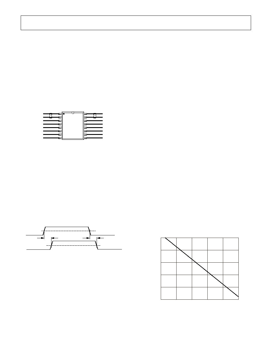
PIN CONFIGURATIONS AND PIN FUNCTION DESCRIPTIONS
1
16
2
15
3
14
4
13
5
12
6
11
7
10
8
9
NC = NO CONNECT
ADuM1400
TOP VIEW
(Not to Scale)
03786-0-005
V
DD1
*GND
1
V
IA
V
IB
V
IC
V
ID
NC
*GND
1
V
DD2
GND
2
*
V
OA
V
OB
V
OC
V
OD
V
E2
GND
2
*
Figure 5. ADuM1400 Pin Configuration
1
16
2
15
3
14
4
13
5
12
6
11
7
10
8
9
ADuM1401
TOP VIEW
(Not to Scale)
03786-0-006
V
DD1
*GND
1
V
IA
V
IB
V
IC
V
OD
V
E1
*GND
1
V
DD2
GND
2
*
V
OA
V
OB
V
OC
V
ID
V
E2
GND
2
*
Figure 6. ADuM1401 Pin Configuration
1
16
2
15
3
14
4
13
5
12
6
11
7
10
8
9
ADuM1402
TOP VIEW
(Not to Scale)
03786-0-007
V
DD1
*GND
1
V
IA
V
IB
V
OC
V
OD
V
E1
*GND
1
V
DD2
GND
2
*
V
OA
V
OB
V
IC
V
ID
V
E2
GND
2
*
Figure 7. ADuM1402 Pin Configuration
* Pins 2 and 8 are internally connected. Connecting both to GND
1
is recommended. Pins 9 and 15 are internally connected. Connecting both to GND
2
is recommended.
Output enable Pin 10 on the ADuM1400 may be left disconnected if outputs are to be always enabled. Output enable Pins 7 and 10 on the ADuM1401/ADuM1402
may be left disconnected if outputs are to be always enabled. In noisy environments, connecting Pin 7 (for ADuM1401 and ADuM1402) and Pin 10 (for all models) to
an external logic high or low is recommended.
Table 11. ADuM1400 Pin Function Descriptions
Pin
No. Mnemonic Function
1 V
DD1
Supply Voltage for Isolator Side 1, 2.7 V to 5.5 V.
2 GND
1
Ground 1. Ground reference for isolator Side 1.
3 V
IA
Logic Input A.
4 V
IB
Logic Input B.
5 V
IC
Logic Input C.
6 V
ID
Logic Input D.
7 NC
No
Connect.
8 GND
1
Ground 1. Ground reference for isolator Side 1.
9 GND
2
Ground 2. Ground reference for isolator Side 2.
10 V
E2
Output Enable 2. Active high logic input. V
OA
, V
OB
, V
OC
, and V
OD
outputs are enabled when V
E2
is high or disconnected. V
OA
, V
OB
, V
OC
, and
V
OD
outputs are disabled when V
E2
is low. In noisy environments, connecting V
E2
to an external logic high or low is recommended.
11 V
OD
Logic Output D.
12 V
OC
Logic Output C.
13 V
OB
Logic Output B.
14 V
OA
Logic Output A.
15 GND
2
Ground 2. Ground reference for isolator Side 2.
16 V
DD2
Supply Voltage for Isolator Side 2, 2.7 V to 5.5 V.

ADuM1400/ADuM1401/ADuM1402
Rev. B | Page 16 of 24
Table 12. ADuM1401 Pin Function Descriptions
Pin
No. Mnemonic Function
1 V
DD1
Supply Voltage for Isolator Side 1, 2.7 V to 5.5 V.
2 GND
1
Ground 1. Ground reference for isolator Side 1.
3 V
IA
Logic Input A.
4 V
IB
Logic Input B.
5 V
IC
Logic Input C.
6 V
OD
Logic Output D.
7 V
E1
Output Enable 1. Active high logic input. V
OD
output is enabled when V
E1
is
high or disconnected. V
OD
is disabled when V
E1
is low. In
noisy environments, connecting V
E1
to an external logic high or low is recommended.
8 GND
1
Ground 1. Ground reference for isolator Side 1.
9 GND
2
Ground 2. Ground reference for isolator Side 2.
10 V
E2
Output Enable 2. Active high logic input. V
OA
, V
OB
, and V
OC
outputs are enabled when V
E2
is
high or disconnected. V
OA
, V
OB
, and V
OC
outputs are disabled when V
E2
is low. In noisy environments, connecting V
E2
to an external logic high or low is recommended.
11 V
ID
Logic Input D.
12 V
OC
Logic Output C.
13 V
OB
Logic Output B.
14 V
OA
Logic Output A.
15 GND
2
Ground 2. Ground reference for isolator Side 2.
16 V
DD2
Supply Voltage for Isolator Side 1, 2.7 V to 5.5 V.
Table 13. ADuM1402 Pin Function Descriptions
Pin
No. Mnemonic Function
1 V
DD1
Supply Voltage for Isolator Side 1, 2.7 V to 5.5 V.
2 GND
1
Ground 1. Ground reference for isolator Side 1.
3 V
IA
Logic Input A.
4 V
IB
Logic Input B.
5 V
OC
Logic Output C.
6 V
OD
Logic Output D.
7 V
E1
Output Enable 1. Active high logic input. V
OC
and V
OD
outputs are enabled when V
E1
is
high or disconnected. V
OC
and V
OD
outputs are
disabled when V
E1
is low. In noisy environments, connecting V
E1
to an external logic high or low is recommended.
8 GND
1
Ground 1. Ground reference for isolator Side 1.
9 GND
2
Ground 2. Ground reference for isolator Side 2.
10 V
E2
Output Enable 2. Active high logic input. V
OA
and V
OB
outputs are enabled when V
E2
is
high or disconnected. V
OA
and V
OB
outputs are
disabled when V
E2
is low. In noisy environments, connecting V
E2
to an external logic high or low is recommended.
11 V
ID
Logic Input D.
12 V
IC
Logic Input C.
13 V
OB
Logic Output B.
14 V
OA
Logic Output A.
15 GND
2
Ground 2. Ground Reference for Isolator Side 2.
16 V
DD2
Supply Voltage for Isolator Side 2, 2.7 V to 5.5 V.
ADuM1400/ADuM1401/ADuM1402
Rev. B | Page 17 of 24
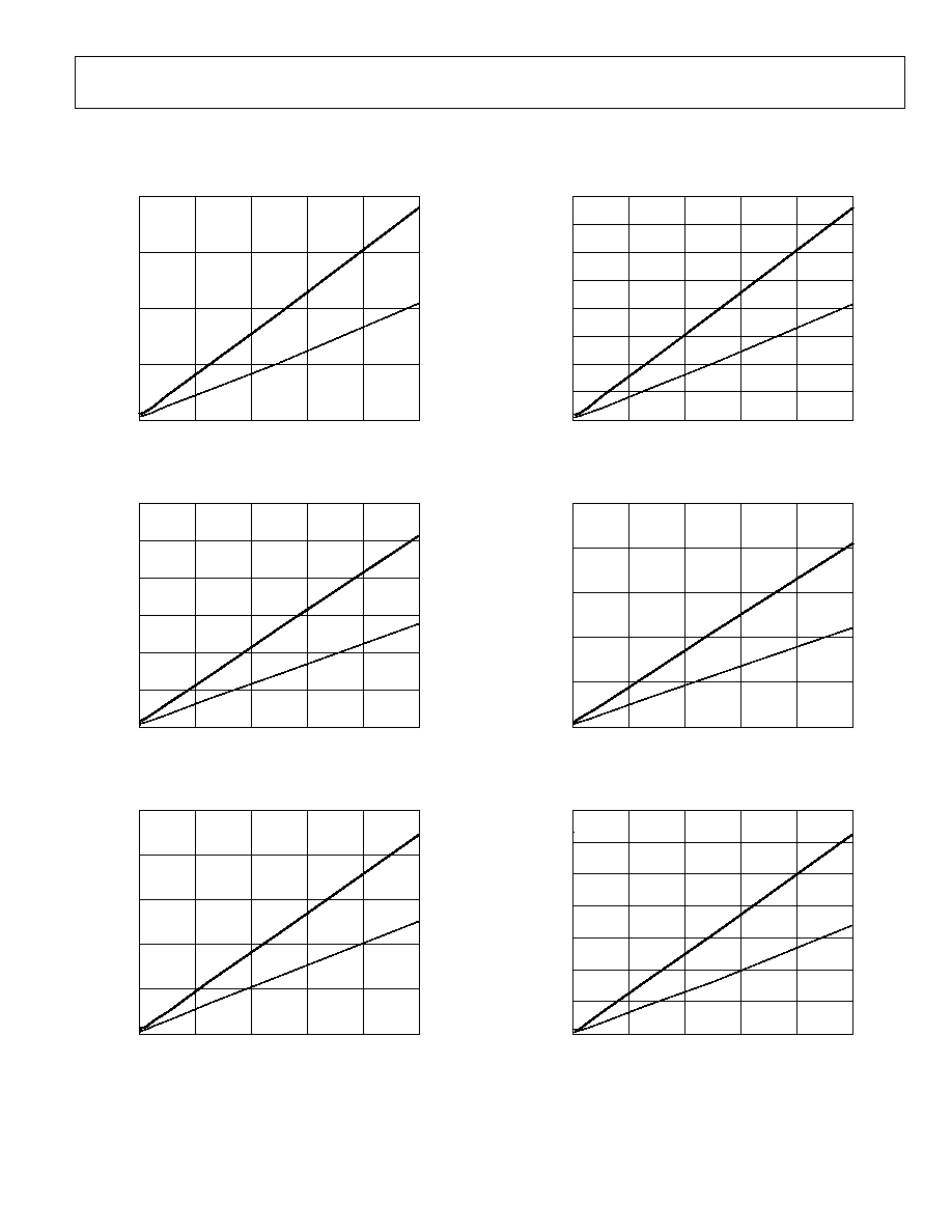
TYPICAL PERFORMANCE CHARACTERISTICS
04407-0-011
DATA RATE (Mbps)
CURRE
NT/CHANNE
L (mA)
0
0
10
5
15
20
20
60
80
40
100
5V
3V
Figure 8. Typical Input Supply Current per Channel vs. Data Rate
for 5 V and 3 V Operation
04407-0-012
DATA RATE (Mbps)
CURRE
NT/CHANNE
L (mA)
0
0
3
2
1
4
5
6
20
60
80
40
100
5V
3V
Figure 9. Typical Output Supply Current per Channel vs. Data Rate
for 5 V and 3 V Operation (No Output Load)
04407-0-013
DATA RATE (Mbps)
CURRE
NT/CHANNE
L (mA)
0
0
6
4
2
8
10
20
60
80
40
100
5V
3V
Figure 10. Typical Output Supply Current per Channel vs. Data Rate
for 5 V and 3 V Operation (15 pF Output Load)
04407-0-014
DATA RATE (Mbps)
CURRE
NT (mA)
0
0
40
50
20
10
30
60
70
80
20
60
80
40
100
5V
3V
Figure 11. Typical ADuM1400 V
DD1
Supply Current vs. Data Rate
for 5 V and 3 V Operation
04407-0-015
DATA RATE (Mbps)
CURRE
NT (mA)
0
0
10
10
5
15
20
20
60
80
40
100
5V
3V
Figure 12. Typical ADuM1400 V
DD2
Supply Current vs. Data Rate
for 5 V and 3 V Operation
04407-0-016
DATA RATE (Mbps)
CURRE
NT (mA)
0
0
25
20
15
10
5
30
50
20
60
80
40
100
5V
3V
Figure 13. Typical ADuM1401 V
DD1
Supply Current vs. Data Rate
for 5 V and 3 V Operation
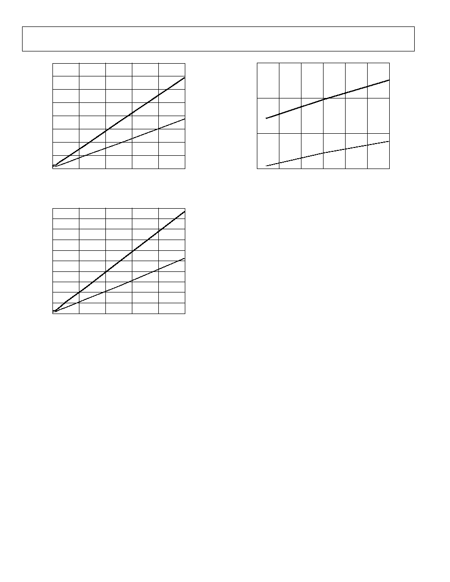
ADuM1400/ADuM1401/ADuM1402
Rev. B | Page 18 of 24
04407-0-017
DATA RATE (Mbps)
CURRE
NT (mA)
0
0
20
15
10
5
30
25
35
40
20
60
80
40
100
5V
3V
Figure 14. Typical ADuM1401 V
DD2
Supply Current vs. Data Rate
for 5 V and 3 V Operation
04407-0-018
DATA RATE (Mbps)
CURRE
NT (mA)
0
0
25
20
15
10
5
45
40
35
30
50
20
60
80
40
100
5V
3V
Figure 15. Typical ADuM1402 V
DD1
or V
DD2
Supply Current vs.
Data Rate for 5 V and 3 V Operation
TEMPERATURE (°C)
P
R
OP
AGATION DE
LAY
(ns
)
50
25
25
30
35
40
0
50
75
25
100
03786-0-023
3V
5V
Figure 16. Propagation Delay vs. Temperature, C Grade
ADuM1400/ADuM1401/ADuM1402
Rev. B | Page 19 of 24
APPLICATION INFORMATION
PC BOARD LAYOUT
The ADuM140x digital isolator requires no external interface
circuitry for the logic interfaces. Power supply bypassing is
strongly recommended at the input and output supply pins
(Figure 17). Bypass capacitors are most conveniently connected
between Pins 1 and 2 for V
DD1
and between Pins 15 and 16 for
V
DD2
. The capacitor value should be between 0.01 µF and 0.1 µF.
The total lead length between both ends of the capacitor and
the input power supply pin should not exceed 20 mm. Bypass-
ing between Pins 1 and 8 and between Pins 9 and 16 should also
be considered unless the ground pair on each package side is
connected close to the package.
V
DD1
GND
1
V
IA
V
IB
V
IC/OC
V
ID/OD
V
E1
GND
1
V
DD2
GND
2
V
OA
V
OB
V
OC/IC
V
OD/ID
V
E2
GND
2
03786-0-019
Figure 17. Recommended Printed Circuit Board Layout
In applications involving high common-mode transients, care
should be taken to ensure that board coupling across the isola-
tion barrier is minimized. Furthermore, the board layout should
be designed such that any coupling that does occur equally
affects all pins on a given component side. Failure to ensure this
could cause voltage differentials between pins exceeding the
device's Absolute Maximum Ratings, thereby leading to latch-up
or permanent damage.
PROPAGATION DELAY-RELATED PARAMETERS
Propagation delay is a parameter that describes the time it takes
a logic signal to propagate through a component. The propaga-
tion delay to a logic low output may differ from the propagation
delay to a logic high.
INPUT (V
IX
)
OUTPUT (V
OX
)
t
PLH
t
PHL
50%
50%
03786-0-020
Figure 18. Propagation Delay Parameters
Pulse-width distortion is the maximum difference between
these two propagation delay values and is an indication of how
accurately the input signal's timing is preserved.
Channel-to-channel matching refers to the maximum that
amount the propagation delay differs between channels within a
single ADuM140x component.
Propagation delay skew refers to the maximum that amount the
propagation delay differs between multiple ADuM140x compo-
nents operating under the same conditions.
DC CORRECTNESS AND MAGNETIC FIELD IMMUNITY
Positive and negative logic transitions at the isolator input
cause narrow (~1 ns) pulses to be sent to the decoder via the
transformer. The decoder is bistable and is, therefore, either set
or reset by the pulses, indicating input logic transitions. In the
absence of logic transitions at the input for more than 2 µs, a
periodic set of refresh pulses indicative of the correct input state
are sent to ensure dc correctness at the output. If the decoder
receives no internal pulses of more than about 5 µs, the input
side is assumed to be unpowered or nonfunctional, in which
case the isolator output is forced to a default state (see Table 10)
by the watchdog timer circuit.
The limitation on the ADuM140x's magnetic field immunity is
set by the condition in which induced voltage in the transformer's
receiving coil is sufficiently large to either falsely set or reset the
decoder. The following analysis defines the conditions under
which this may occur. The 3 V operating condition of the
ADuM140x is examined because it represents the most
susceptible mode of operation.
The pulses at the transformer output have an amplitude greater than
1.0 V. The decoder has a sensing threshold at about 0.5 V, therefore
establishing a 0.5 V margin in which induced voltages can be toler-
ated. The voltage induced across the receiving coil is given by
V = (d/dt)
r
n
2
;
n = 1, 2,..., N
where:
is magnetic flux density (gauss).
N is the number of turns in the receiving coil.
r
n
is the radius of the n
th
turn in the receiving coil (cm).
Given the geometry of the receiving coil in the ADuM140x and
an imposed requirement that the induced voltage be at most
50% of the 0.5 V margin at the decoder, a maximum allowable
magnetic field is calculated as shown in Figure 19.
MAGNETIC FIELD FREQUENCY (Hz)
100.000
MAX
I
MUM ALLO
WABLE
MAG
N
E
T
IC FLUX
DE
NS
ITY
(k
ga
us
s
)
0.001
1M
10.000
0.010
1k
10k
10M
0.100
1.000
100M
100k
03786-0-021
Figure 19. Maximum Allowable External Magnetic Flux Density
ADuM1400/ADuM1401/ADuM1402
Rev. B | Page 20 of 24
For example, at a magnetic field frequency of 1 MHz, the
maximum allowable magnetic field of 0.2 kgauss induces a
voltage of 0.25 V at the receiving coil. This is about 50% of the
sensing threshold and does not cause a faulty output transition.
Similarly, if such an event were to occur during a transmitted
pulse (and was of the worst-case polarity), it would reduce the
received pulse from > 1.0 V to 0.75 V--still well above the 0.5 V
sensing threshold of the decoder.
The preceding magnetic flux density values correspond to specific
current magnitudes at given distances from the ADuM140x trans-
formers.
Figure 20
expresses these allowable current magnitudes as
a function of frequency for selected distances. As seen, the
ADuM140x is extremely immune and can be affected only by ex-
tremely large currents operated at high frequency, very close to the
component. For the 1 MHz example noted, one would have to place
a 0.5 kA current 5 mm away from the ADuM140x to affect the
component's operation.
MAGNETIC FIELD FREQUENCY (Hz)
MAX
I
MUM ALLOWABLE
CURRE
NT (k
A)
1000.00
100.00
10.00
1.00
0.10
0.01
1k
10k
100M
100k
1M
10M
DISTANCE = 5mm
DISTANCE = 1m
DISTANCE = 100mm
03786-0-022
Figure 20. Maximum Allowable Current
for Various Current-to-ADuM140x Spacings
Note that at combinations of strong magnetic field and high
frequency, any loops formed by printed circuit board traces
could induce sufficiently large error voltages to trigger the
thresholds of succeeding circuitry. Care should be taken in the
layout of such traces to avoid this possibility.
POWER CONSUMPTION
The supply current at a given channel of the ADuM140x isola-
tor is a function of the supply voltage, the channel's data rate,
and the channel's output load.
For each input channel, the supply current is given by
I
DDI
= I
DDI (Q)
f 0.5f
r
I
DDI
= I
DDI (D)
× (2f f
r
) + I
DDI (Q)
f > 0.5f
r
For each output channel, the supply current is given by
I
DDO
= I
DDO (Q)
f 0.5f
r
I
DDO
= (I
DDO (D)
+ (0.5 × 10
-3
) × C
L
V
DDO
) × (2f f
r
) + I
DDO (Q)
f > 0.5f
r
where:
I
DDI (D)
, I
DDO (D)
are the input and output dynamic supply currents
per channel (mA/Mbps).
C
L
is output load capacitance (pF).
V
DDO
is the output supply voltage (V).
f is the input logic signal frequency (MHz, half of the input data
rate, NRZ signaling).
f
r
is the input stage refresh rate (Mbps).
I
DDI (Q)
, I
DDO (Q)
are the specified input and output quiescent sup-
ply currents (mA).
To calculate the total I
DD1
and I
DD2
supply current, the supply
currents for each input and output channel corresponding to
I
DD1
and I
DD2
are calculated and totaled. Figure 8 and Figure 9
provide per-channel supply currents as a function of data rate
for an unloaded output condition. Figure 10 provides per-
channel supply current as a function of data rate for a 15 pF
output condition. Figure 11 through Figure 14 provide total
I
DD1
and I
DD2
supply current as a function of data rate for
ADuM1400/ADuM1401/ADuM1402 channel configurations.
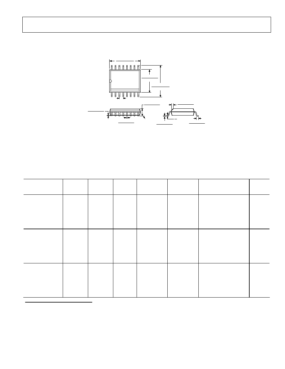
ADuM1400/ADuM1401/ADuM1402
Rev. B | Page 21 of 24
OUTLINE DIMENSIONS
CONTROLLING DIMENSIONS ARE IN MILLIMETERS; INCH DIMENSIONS
(IN PARENTHESES) ARE ROUNDED-OFF MILLIMETER EQUIVALENTS FOR
REFERENCE ONLY AND ARE NOT APPROPRIATE FOR USE IN DESIGN
COMPLIANT TO JEDEC STANDARDS MS-013AA
SEATING
PLANE
0.30 (0.0118)
0.10 (0.0039)
0.51 (0.0201)
0.31 (0.0122)
2.65 (0.1043)
2.35 (0.0925)
1.27 (0.0500)
BSC
16
9
8
1
10.65 (0.4193)
10.00 (0.3937)
7.60 (0.2992)
7.40 (0.2913)
10.50 (0.4134)
10.10 (0.3976)
8°
0°
0.75 (0.0295)
0.25 (0.0098)
×
45°
1.27 (0.0500)
0.40 (0.0157)
0.33 (0.0130)
0.20 (0.0079)
COPLANARITY
0.10
Figure 21. 16-Lead Standard Small Outline Package [SOIC]
Wide Body (RW-16)
Dimension shown in millimeters (inches)
ORDERING GUIDE
Model
Number of
Inputs,
V
DD1
Side
Number of
Inputs,
V
DD2
Side
Maximum
Data Rate
(Mbps)
Maximum
Propagation
Delay, 5 V (ns)
Maximum
Pulse-Width
Distortion (ns) Temperature Range (°C)
Package
Option
1
ADuM1400ARW
2
4
0
1
100
40
40 to +105
RW-16
ADuM1400BRW
2
4
0
10
50
3
40 to +105
RW-16
ADuM1400CRW
2
4
0
90
32
2
40 to +105
RW-16
ADuM1400ARWZ
2, 3
4
0
1
100
40
40 to +105
RW-16
ADuM1400BRWZ
2, 3
4
0
10
50
3
40 to +105
RW-16
ADuM1400CRWZ
2, 3
4
0
90
32
2
40 to +105
RW-16
ADuM1401ARW
2
3
1
1
100
40
40 to +105
RW-16
ADuM1401BRW
2
3
1
10
50
3
40 to +105
RW-16
ADuM1401CRW
2
3
1
90
32
2
40 to +105
RW-16
ADuM1401ARWZ
2, 3
3
1
1
100
40
40 to +105
RW-16
ADuM1401BRWZ
2, 3
3
1
10
50
3
40 to +105
RW-16
ADuM1401CRWZ
2, 3
3
1
90
32
2
40 to +105
RW-16
ADuM1402ARW
2
2
2
1
100
40
40 to +105
RW-16
ADuM1402BRW
2
2
2
10
50
3
40 to +105
RW-16
ADuM1402CRW
2
2
2
90
32
2
40 to +105
RW-16
ADuM1402ARWZ
2, 3
2
2
1
100
40
40 to +105
RW-16
ADuM1402BRWZ
2, 3
2
2
10
50
3
40 to +105
RW-16
ADuM1402CRWZ
2, 3
2
2
90
32
2
40 to +105
RW-16
1
RW-16 = 16-lead wide body SOIC.
2
Tape and reel are available. The addition of an "-RL" suffix designates a 13" (1,000 units) tape and reel option.
3
Z = Pb-free part.

ADuM1400/ADuM1401/ADuM1402
Rev. B | Page 22 of 24
NOTES

ADuM1400/ADuM1401/ADuM1402
Rev. B | Page 23 of 24
NOTES

ADuM1400/ADuM1401/ADuM1402
Rev. B | Page 24 of 24
NOTES
© 2004 Analog Devices, Inc. All rights reserved. Trademarks and
regis-
tered trademarks are the property of their respective owners.
C0378606/04(B)
Document Outline
- FEATURES
- APPLICATIONS
- GENERAL DESCRIPTION
- FUNCTIONAL BLOCK DIAGRAMS
- TABLE OF CONTENTS
- þÿ
- þÿ
- þÿ
- þÿ
- þÿ
- þÿ