ADuM1230 Isolated Half-Bridge Driver, 0.1 A Amp Output Data Sheet (Rev. A)
Isolated Half-Bridge Driver,
0.1 A Amp Output
ADuM1230
Rev. A
Information furnished by Analog Devices is believed to be accurate and reliable. However, no
responsibility is assumed by Analog Devices for its use, nor for any infringements of patents or other
rights of third parties that may result from its use. Specifications subject to change without notice. No
license is granted by implication or otherwise under any patent or patent rights of Analog Devices.
Trademarks and registered trademarks are the property of their respective owners.
One Technology Way, P.O. Box 9106, Norwood, MA 02062-9106, U.S.A.
Tel: 781.329.4700
www.analog.com
Fax: 781.461.3113
© 2005 Analog Devices, Inc. All rights reserved.
FEATURES
Isolated high-side and low-side outputs
High-side or low-side relative to input: ±700 V
PEAK
High-side/low-side differential: 700 V
PEAK
0.1 A peak output current
High frequency operation: 5 MHz max
High common-mode transient immunity: >50 kV/s
High temperature operation: 105°C
Wide body, 16-lead SOIC
UL1577 2500 V rms input-to-output withstand voltage
APPLICATIONS
Isolated IGBT/MOSFET gate drives
Plasma displays
Industrial inverters
Switching power supplies
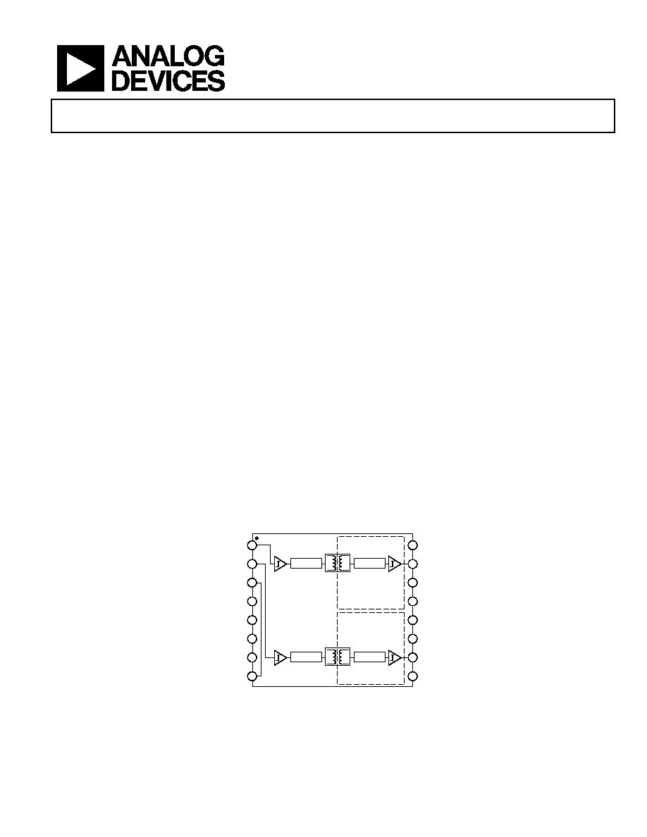
GENERAL DESCRIPTION
The ADuM1230
1
is an isolated half-bridge gate driver that
employs Analog Devices' iCoupler® technology to provide
independent and isolated high-side and low-side outputs.
Combining high speed CMOS and monolithic transformer
technology, this isolation component provides outstanding
performance characteristics superior to optocoupler-based
solutions.
By avoiding the use of LEDs and photodiodes, this iCoupler
gate drive device is able to provide precision timing characteristics
not possible with optocouplers. Furthermore, the reliability and
performance stability problems associated with optocoupler
LEDs are avoided.
In comparison to gate drivers employing high voltage level
translation methodologies, the ADuM1230 offers the benefit of
true, galvanic isolation between the input and each output. Each
output may be operated up to ±700 V
P
relative to the input,
thereby supporting low-side switching to negative voltages. The
differential voltage between the high-side and low-side can be
as high as 700 V
P
.
As a result, the ADuM1230 provides reliable control over the
switching characteristics of IGBT/MOSFET configurations over
a wide range of positive or negative switching voltages.
1
Protected by U.S. Patents 5,952,849 6,873,065, and other pending patents.
FUNCTIONAL BLOCK DIAGRAM
ENCODE
DECODE
ENCODE
DECODE
DISABLE
NC
NC
V
DD1
NC
V
DDB
V
OB
GND
B
5
6
7
8
12
11
GND
1
NC
4
13
V
DD1
GND
A
3
14
V
IB
V
OA
2
15
V
IA
V
DDA
1
16
10
9
05
460
-
00
1
Figure 1.

ADuM1230
Rev. A | Page 2 of 12
TABLE OF CONTENTS
Features .............................................................................................. 1
Applications....................................................................................... 1
General Description ......................................................................... 1
Functional Block Diagram .............................................................. 1
Revision History ............................................................................... 2
Specifications..................................................................................... 3
Electrical Characteristics............................................................. 3
Package Characteristics ............................................................... 4
Regulatory Information............................................................... 4
Insulation and Safety-Related Specifications............................ 4
Recommended Operating Conditions ...................................... 4
Absolute Maximum Ratings ............................................................5
ESD Caution...................................................................................5
Pin Configuration and Function Descriptions..............................6
Typical Performance Characteristics ..............................................7
Application Notes ..............................................................................8
Common-Mode Transient Immunity ........................................8
Typical Application Usage............................................................9
Outline Dimensions ....................................................................... 10
Ordering Guide .......................................................................... 10
REVISION HISTORY
12/05--Rev. Sp0 to Rev. A
Changes to Figure 1 and Note 1...................................................... 1
Added Typical Application Usage Section .................................... 9
Inserted Figure 14............................................................................. 9
5/05--Revision Sp0: Initial Version

ADuM1230
Rev. A | Page 3 of 12
SPECIFICATIONS
ELECTRICAL CHARACTERISTICS
All voltages are relative to their respective ground. 4.5 V V
DD1
5.5 V, 12 V V
DDA
18 V, 12 V V
DDB
18 V. All min/max
specifications apply over the entire recommended operating range, unless otherwise noted. All typical specifications are at T
A
= 25°C,
V
DD1
= 5 V, V
DDA
= 15 V, V
DDB
= 15 V.
Table 1.
Parameter
Symbol
Min
Typ
Max
Unit
Test Conditions
DC SPECIFICATIONS
Input Supply Current, Quiescent
I
DDI (Q)
4.0
mA
Output Supply Current, A or B, Quiescent
I
DDA (Q)
,
I
DDB (Q)
1.2
mA
Input Supply Current, 10 Mbps
I
DDI (10)
8.0
mA
Output Supply Current, A or B, 10 Mbps
I
DDA (10)
,
I
DDB (10)
22
mA
C
L
= 200 pF
Input Currents
I
IA
, I
IB
, I
DISABLE
-10
+0.01
+10
A
0 V
IA
, V
IB
, V
DISABLE
V
DD1
Logic High Input Threshold
V
IH
2.0
V
Logic Low Input Threshold
V
IL
0.8
V
Logic High Output Voltages
V
OAH
, V
OBH
V
DDA
- 0.1,
V
DDB
- 0.1
V
DDA
, V
DDB
V
I
OA
, I
OB
= -1 mA
Logic Low Output Voltages
V
OAL
, V
OBL
0.1
V
I
OA
, I
OB
= 1 mA
Output Short-Circuit Pulsed Current
1
I
OA (SC)
, I
OB (SC)
100
mA
SWITCHING SPECIFICATIONS
Minimum Pulse Width
2
PW
100
ns
C
L
= 200 pF
Maximum Switching Frequency
3
10
Mbps
C
L
= 200 pF
Propagation Delay
4
t
PHL
, t
PLH
97
124
160
ns
C
L
= 200 pF
Change vs. Temperature
100
ps/°C
Pulse Width Distortion, |t
PLH
- t
PHL
|
PWD
8
ns
C
L
= 200 pF
Channel-to-Channel Matching,
Rising or Falling Edges
5
5
ns
C
L
= 200 pF
Channel-to-Channel Matching,
Rising vs. Falling Edges
6
13
ns
C
L
= 200 pF
Part-to-Part Matching, Rising or Falling Edges
7
55
ns
C
L
= 200 pF
Part-to-Part Matching, Rising vs. Falling Edges
8
63
ns
C
L
= 200 pF
Output Rise/Fall Time (10% to 90%)
t
R
/t
F
20
ns
C
L
= 200 pF
1
Short-circuit duration less than 1 second. Average power must conform to the limit shown under the Absolute Maximum Ratings.
2
The minimum pulse width is the shortest pulse width at which the specified timing parameters are guaranteed.
3
The maximum switching frequency is the maximum signal frequency at which the specified timing parameters are guaranteed.
4
t
PHL
propagation delay is measured from the 50% level of the falling edge of the V
Ix
signal to the 50% level of the falling edge of the V
Ox
signal. t
PLH
propagation delay is
measured from the 50% level of the rising edge of the V
Ix
signal to the 50% level of the rising edge of the V
Ox
signal.
5
Channel-to-channel matching, rising vs. falling edges is the magnitude of the propagation delay difference between two channels of the same part when the inputs
are either both rising edges or falling edges. The supply voltages and the loads on each channel are equal.
6
Channel-to-channel matching, rising or falling edges is the magnitude of the propagation delay difference between two channels of the same part when one input is
a rising edge and the other input is a falling edge. The supply voltages and loads on each channel are equal.
7
Part-to-part matching, rising or falling edges is the magnitude of the propagation delay difference between the same channels of two different parts when the inputs
are either both rising or falling edges. The supply voltages, temperatures, and loads of each part are equal.
8
Part-to-part matching, rising vs. falling edges is the magnitude of the propagation delay difference between the same channels of two different parts when one input
is a rising edge and the other input is a falling edge. The supply voltages, temperatures, and loads of each part are equal.

ADuM1230
Rev. A | Page 4 of 12
PACKAGE CHARACTERISTICS
Table 2.
Parameter
Symbol
Min
Typ
Max
Unit
Test Conditions
Resistance (Input-to-Output)
1
R
I-O
10
12
Capacitance (Input-to-Output)
1
C
I-O
2.0
pF
f = 1 MHz
Input Capacitance
C
I
4.0
pF
IC Junction-to-Ambient Thermal Resistance
JCa
76
°C/W
1
The device is considered a 2-terminal device: Pins 1 through 8 are shorted together, and Pins 9 through 16 are shorted together.
REGULATORY INFORMATION
The ADuM1230 is approved, as shown in Table 3.
Table 3.
UL
1
Recognized under 1577 component recognition program
1
In accordance with UL1577, each ADuM1230 is proof tested by applying an insulation test voltage 3000 V rms for 1 second (current leakage detection limit = 5 A).
INSULATION AND SAFETY-RELATED SPECIFICATIONS
Table 4.
Parameter
Symbol
Value
Unit
Conditions
Rated Dielectric Insulation Voltage
2500
V rms
1 minute duration
Minimum External Air Gap (Clearance)
L(I01)
7.7 min
mm
Measured from input terminals to output terminals,
shortest distance through air
Minimum External Tracking (Creepage)
L(I02)
8.1 min
mm
Measured from input terminals to output terminals,
shortest distance path along body
Minimum Internal Gap (Internal Clearance)
0.017 min
mm
Insulation distance through insulation
Tracking Resistance (Comparative Tracking Index)
CTI
>175
V
DIN IEC 112/VDE 0303 Part 1
Isolation Group
IIIa
Material Group (DIN VDE 0110, 1/89, Table 1)
RECOMMENDED OPERATING CONDITIONS
Table 5.
Parameter
Symbol
Min
Max
Unit
Operating Temperature
T
A
-40
+105
°C
Input Supply Voltage
1
V
DD1
4.5
5.5
V
Output Supply Voltages
1
V
DDA
, V
DDB
12 18 V
Input Signal Rise and Fall Times
1
ms
Common-Mode Transient Immunity, Input-to-Output
2
-50
+50
kV/s
Common-Mode Transient Immunity, Between Outputs
2
-50
+50
kV/s
Transient Immunity, Supply Voltages
2
-50
+50
kV/s
1
All voltages are relative to their respective ground.
2
See the Common-Mode Transient Immunity section for transient diagrams and additional information.
ADuM1230
Rev. A | Page 5 of 12
ABSOLUTE MAXIMUM RATINGS
Table 6.
Parameter
Symbol
Min
Max
Unit
Storage Temperature
T
ST
-55
+150
°C
Ambient Operating
Temperature
T
A
-40
+105
°C
Input Supply Voltage
1
V
DD1
-0.5
+7.0
V
Output Supply Voltage
1
V
DDA
, V
DDB
-0.5 +27
V
Input Voltage
1
V
IA
, V
IB
-0.5
V
DDI
+ 0.5
V
Output Voltage
1
V
OA
, V
OB
-0.5
V
DDA
+ 0.5,
V
DDB
+ 0.5
V
Input-Output Voltage
2
-700
+700
V
PEAK
Output Differential
Voltage
3
700
V
PEAK
Output DC Current
I
OA
, I
OB
-20 +20
mA
Common-Mode
Transients
4
-100
+100
kV/s
1
All voltages are relative to their respective ground.
2
Input-to-output voltage is defined as GND
A
- GND
1
or GND
B
- GND
1
.
3
Output differential voltage is defined as GND
A
- GND
B
.
4
Refers to common-mode transients across any insulation barrier. Common-
mode transients exceeding the Absolute Maximum Ratings can cause latch-
up or permanent damage.
Stresses above those listed under Absolute Maximum Ratings
may cause permanent damage to the device. This is a stress
rating only; functional operation of the device at these or any
other conditions above those listed in the operational sections
of this specification is not implied. Exposure to absolute
maximum rating conditions for extended periods may affect
device reliability.
Ambient temperature = 25°C, unless otherwise noted.
Table 7. ADuM1230 Truth Table (Positive Logic)
V
IA
/V
IB
Input
V
DD1
State
DISABLE
V
OA
/V
OB
Output
Notes
H
Powered
L
H
L
Powered
L
L
X
Unpowered
X
L
Output returns to input state within 1 s of V
DDI
power restoration.
X Powered
H
L
ESD CAUTION
ESD (electrostatic discharge) sensitive device. Electrostatic charges as high as 4000 V readily accumulate on
the human body and test equipment and can discharge without detection. Although this product features
proprietary ESD protection circuitry, permanent damage may occur on devices subjected to high energy
electrostatic discharges. Therefore, proper ESD precautions are recommended to avoid performance
degradation or loss of functionality.
ADuM1230
Rev. A | Page 6 of 12
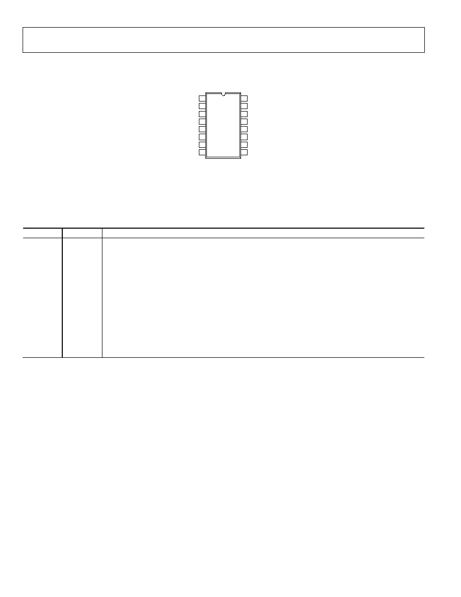
PIN CONFIGURATION AND FUNCTION DESCRIPTIONS
05
46
0
-0
0
2
V
IA 1
V
IB 2
V
DD1
3
GND
1
4
V
DDA
16
V
OA
15
GND
A
14
NC
13
DISABLE
5
NC
12
NC
6
V
DDB
11
NC
7
V
OB
10
V
DD1
8
GND
B
9
NC = NO CONNECT
ADuM1230
TOP VIEW
(Not to Scale)
Figure 2. Pin Configuration
Note that Pin 3 and Pin 8 are internally connected. Connecting both to V
DD1
is recommended. Pin 12 and Pin 13 are floating and
should be left unconnected.
Table 8. Pin Function Descriptions
Pin No.
Mnemonic
Function
1 V
IA
Logic Input A.
2 V
IB
Logic Input B.
3 V
DD1
Input Supply Voltage, 4.5 V to 5.5 V.
4 GND
1
Ground Reference for Input Logic Signals.
5
DISABLE
Input Disable. Disables the isolator inputs and refresh circuits. Outputs take on default low state.
6, 7, 12, 13
NC
No Connect.
8 V
DD1
Input Supply Voltage, 4.5 V to 5.5 V.
9 GND
B
Ground Reference for Output B.
10 V
OB
Output B.
11 V
DDB
Output B Supply Voltage, 12 V to 18 V.
14 GND
A
Ground Reference for Output A.
15 V
OA
Output A.
16 V
DDA
Output A Supply Voltage, 12 V to 18 V.
ADuM1230
Rev. A | Page 7 of 12
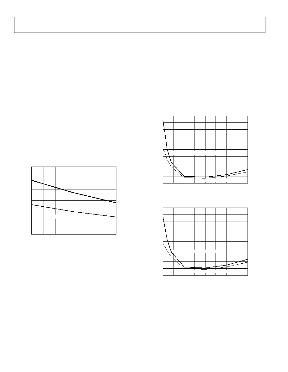
TYPICAL PERFORMANCE CHARACTERISTICS
05
46
0-
00
3
DATA RATE (Mbps)
10
0
4
CU
RRE
NT
(
m
A)
6
5
4
3
2
1
0
Figure 3. Typical Input Supply Current Variation with Data Rate
05
46
0-
00
4
DATA RATE (Mbps)
10
0
4
CU
RRE
NT
(
m
A)
18
16
14
12
8
4
10
6
2
0
Figure 4. Typical Output Supply Current Variation with Data Rate
05
46
0-
0
05
TEMPERATURE (°C)
120
40
40
60
80
100
20
0
20
PR
O
P
A
G
A
TI
ON
D
E
L
A
Y (
n
s)
135
130
125
120
115
Figure 5. Typical Propagation Delay Variation with Temperature
05
46
0-
00
6
OUTPUT SUPPLY VOLTAGE (V)
18
12
15
PR
O
P
A
G
A
TI
O
N
D
E
L
A
Y (
n
s)
129
128
127
126
125
124
123
CH. B, FALLING EDGE
CH. A, FALLING EDGE
CH. A, RISING EDGE
CH. B, RISING EDGE
Figure 6. Typical Propagation Delay Variation with
Output Supply Voltage (Input Supply Voltage = 5.0 V)
05
46
0-
0
07
OUTPUT SUPPLY VOLTAGE (V)
5.5
4.5
5.0
PR
O
P
A
G
A
TI
ON
D
E
L
A
Y (
n
s)
129
128
127
126
125
124
123
CH. B, FALLING EDGE
CH. A, FALLING EDGE
CH. A, RISING EDGE
CH. B, RISING EDGE
Figure 7. Typical Propagation Delay Variation with Input Supply Voltage
(Output Supply Voltage = 15.0 V)
ADuM1230
Rev. A | Page 8 of 12
APPLICATION NOTES
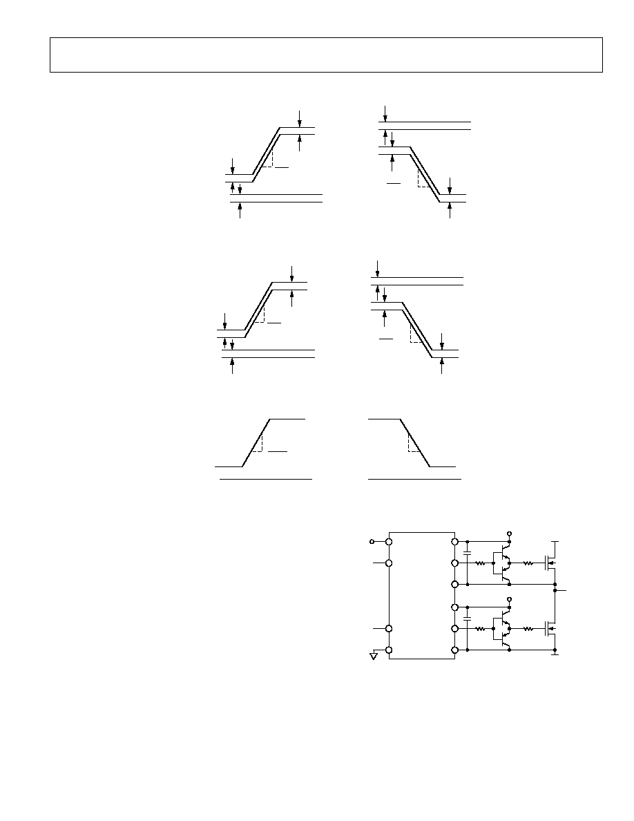
COMMON-MODE TRANSIENT IMMUNITY
In general, common-mode transients consist of linear and
sinusoidal components. The linear component of a common-
mode transient is given by
V
CM, linear
= (V/t) t
where V/t is the slope of the transient shown in Figure 11
and Figure 12.
The transient of the linear component is given by
dV
CM
/dt = V/t
The ADuM1230's ability to operate correctly in the presence of
linear transients is characterized by the data in Figure 8. The
data is based on design simulation and is the maximum linear
transient magnitude that the ADuM1230 can tolerate without
an operational error. This data shows a higher level of robustness
than what is shown in Table 5 because the transient immunity
values obtained in Table 5 use measured data and apply
allowances for measurement error and margin.
05
46
0-
0
1
1
TEMPERATURE (°C)
100
40
0
40
80
20
20
60
T
RANS
I
E
NT
I
M
M
U
NI
T
Y
(
k
V
/
µ
s
)
300
250
200
150
100
50
0
WORST-CASE PROCESS VARIATION
BEST-CASE PROCESS VARIATION
Figure 8. Transient Immunity (Linear Transients) vs. Temperature
The sinusoidal component (at a given frequency) is given by
V
CM, sinusoidal
= V
0
sin(2ft)
where:
V
0
is the magnitude of the sinusoidal.
f is the frequency of the sinusoidal.
The transient magnitude of the sinusoidal component is given by
dV
CM
/dt = 2f V
0
The ADuM1230's ability to operate correctly in the presence
of sinusoidal transients is characterized by the data in Figure 9
and Figure 10. The data is based on design simulation and is
the maximum sinusoidal transient magnitude (2f V
0
) that the
ADuM1230 can tolerate without an operational error. Values
for immunity against sinusoidal transients are not included in
Table 5 because measurements to obtain such values have not
been possible.
05
46
0-
01
2
FREQUENCY (MHz)
2000
0
500
1000
1500
1750
250
750
1250
T
RANS
I
E
NT
I
M
M
U
NI
T
Y
(
k
V
/
µ
s
)
200
160
180
120
80
40
140
100
60
20
0
WORST-CASE PROCESS VARIATION
BEST-CASE PROCESS VARIATION
Figure 9. Transient Immunity (Sinusoidal Transients),
27°C Ambient Temperature
05
46
0-
01
3
FREQUENCY (MHz)
2000
0
500
1000
1500
1750
250
750
1250
T
RANS
I
E
NT
I
M
M
U
NI
T
Y
(
k
V
/
µ
s
)
200
140
100
60
20
160
180
120
80
40
0
WORST-CASE PROCESS VARIATION
BEST-CASE PROCESS VARIATION
Figure 10. Transient Immunity (Sinusoidal Transients),
100°C Ambient Temperature
ADuM1230
Rev. A | Page 9 of 12
GND
1
V
DD1
V
t
V
t
5V
GND
1
V
DD1
15V
15V
GND
A
AND GND
B
V
DDA
AND V
DDB
5V
GND
A
AND GND
B
V
DDA
AND V
DDB
15V
15V
05
46
0-
00
8
Figure 11. Common-Mode Transient Immunity Waveforms--Input to Output
GND
B
/GND
B
V
DDA
/V
DDB
V
t
V
t
15V
GND
B
/GND
B
V
DDA
/V
DDB
15V
15V
GND
A
/GND
B
V
DDA
/V
DDB
15V
GND
A
/GND
B
V
DDA
/V
DDB
15V
15V
0
546
0-
0
09
Figure 12. Common-Mode Transient Immunity Waveforms--Between Outputs
GND
A
/GND
B
V
DDA
/V
DDB
V
DDA
/V
DDB
GND
A
/GND
B
05
46
0-
0
10
V
DD
t
Figure 13. Transient Immunity Waveforms--Output Supplies
TYPICAL APPLICATION USAGE
The ADuM1230 is intended for driving low gate capacitance
transistors (200 pF typically). Most high voltage applications
involve larger transistors than this. To accommodate these
situations, users can choose either a gate driver with a stronger
output stage or the buffer configuration with the ADuM1230, as
shown in Figure 14. In many cases, the buffer configuration is
the less expensive of the two options and provides the greatest
amount of design flexibility. The precise buffer/high voltage
transistor combination can be selected to fit the application's
needs.
FLOATING
V
DDB
FLOATING
V
DDA
V
DDA
V
OA
GND
A
GND
1
V
DDB
V
OB
V
DD1
V
IA
V
IB
GND
B
ADuM1230
+HV
HV
05
46
0-
01
4
Figure 14.

ADuM1230
Rev. A | Page 10 of 12
OUTLINE DIMENSIONS
CONTROLLING DIMENSIONS ARE IN MILLIMETERS; INCH DIMENSIONS
(IN PARENTHESES) ARE ROUNDED-OFF MILLIMETER EQUIVALENTS FOR
REFERENCE ONLY AND ARE NOT APPROPRIATE FOR USE IN DESIGN
COMPLIANT TO JEDEC STANDARDS MS-013-AA
SEATING
PLANE
0.30 (0.0118)
0.10 (0.0039)
0.51 (0.0201)
0.31 (0.0122)
2.65 (0.1043)
2.35 (0.0925)
1.27 (0.0500)
BSC
16
9
8
1
10.65 (0.4193)
10.00 (0.3937)
7.60 (0.2992)
7.40 (0.2913)
10.50 (0.4134)
10.10 (0.3976)
8°
0°
0.75 (0.0295)
0.25 (0.0098)
×
45°
1.27 (0.0500)
0.40 (0.0157)
0.33 (0.0130)
0.20 (0.0079)
COPLANARITY
0.10
Figure 15. 16-Lead Standard Small Outline Package [SOIC_W]
Wide Body (RW-16)
Dimensions shown in millimeters and (inches)
ORDERING GUIDE
Model
No. of
Channels
Output Peak
Current (A)
Output
Voltage (V)
Temperature Range
Package Description
Package
Option
ADuM1230BRWZ
1
2
0.1
15
-40°C to +105°C
16-Lead SOIC_W
RW-16
ADuM1230BRWZ-RL
1
2
0.1
15
-40°C to +105°C
16-Lead SOIC_W,
13-inch Tape and Reel Option
(1, 000 Units)
RW-16
1
Z = Pb-free part.

ADuM1230
Rev. A | Page 11 of 12
NOTES

ADuM1230
Rev. A | Page 12 of 12
T
NOTES
© 2005 Analog Devices, Inc. All rights reserved. Trademarks and
registered trademarks are the property of their respective owners.
D05460-0-12/05(A)
TTT
Document Outline
- þÿ
- þÿ
- GENERAL DESCRIPTION
- þÿ
- þÿ
- þÿ
- þÿ
- þÿ
- PACKAGE CHARACTERISTICS
- þÿ
- þÿ
- þÿ
- þÿ
- þÿ
- þÿ
- þÿ
- þÿ