ADuC7024 Precision Analog Microcontroller 12-bit Analog I/O and PWM, ARM7TDMI® MCU Preliminary Data Sheet (REV. PrC)
Precision Analog Microcontroller
12-bit Analog I/O and PWM, ARM7TDMI® MCU
Preliminary Technical Data
ADuC7024
FEATURES
Analog I/O
10-Channel, 12-bit, 1MSPS ADC
Fully differential and single-ended modes
0 to V
REF
Analog Input Range
Dual 12-bit Voltage Output DACs
On-Chip 20ppm/°C Voltage Reference
On-Chip Temperature Sensor (±3°C)
Uncommitted Voltage Comparator
Microcontroller
ARM7TDMI Core, 16/32-bit RISC architecture
JTAG Port supports code download and debug
Clocking options: - Trimmed On-Chip Oscillator (± 3%)
- External Watch crystal
- External clock source
45MHz PLL with Programmable Divider
Memory
62k Bytes Flash/EE Memory, 8k Bytes SRAM
In-Circuit Download, JTAG based Debug
Software triggered in-circuit re-programmability
On-Chip Peripherals
UART, 2 I
2
C and SPI Serial I/O
30-Pin GPIO Port
2 X General Purpose Timers
Wake-up and Watchdog Timers
Power Supply Monitor
Three-phase 16-bit PWM generator
PLA Programmable Logic (Array)
Power
Specified for 3V operation
Active Mode: 6mW (@1MHz)
300mW (@45MHz)
Packages and Temperature Range
64 Pin LFCSP 9x9mm body package
64 Pin LQFP 12x12mm body package
Fully specified for 40°C to 85°C operation
Tools
Low-Cost QuickStart Development System
Full Third-Party Support
APPLICATIONS
Industrial Control and Automation Systems
Smart Sensors, Precision Instrumentation
Base Station Systems, Optical Networking
(See general description on page 12)
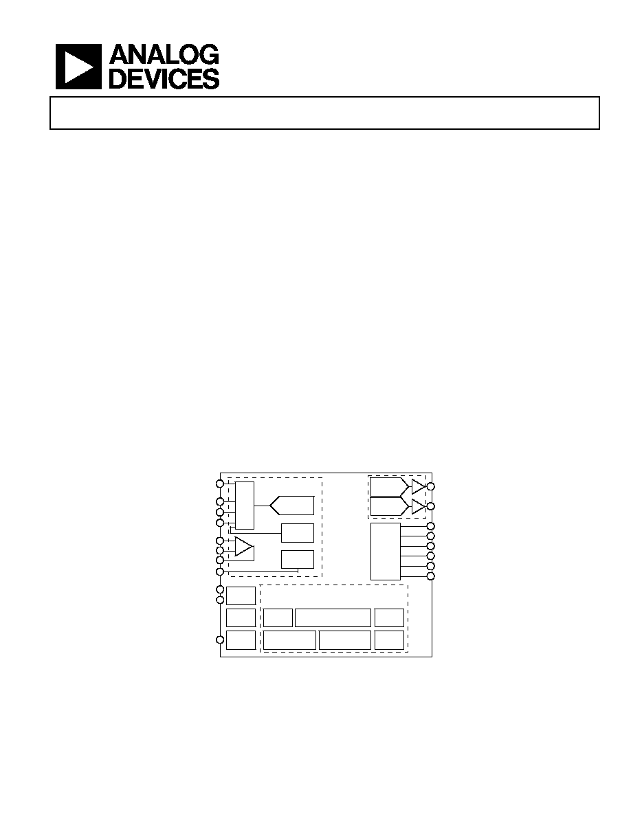
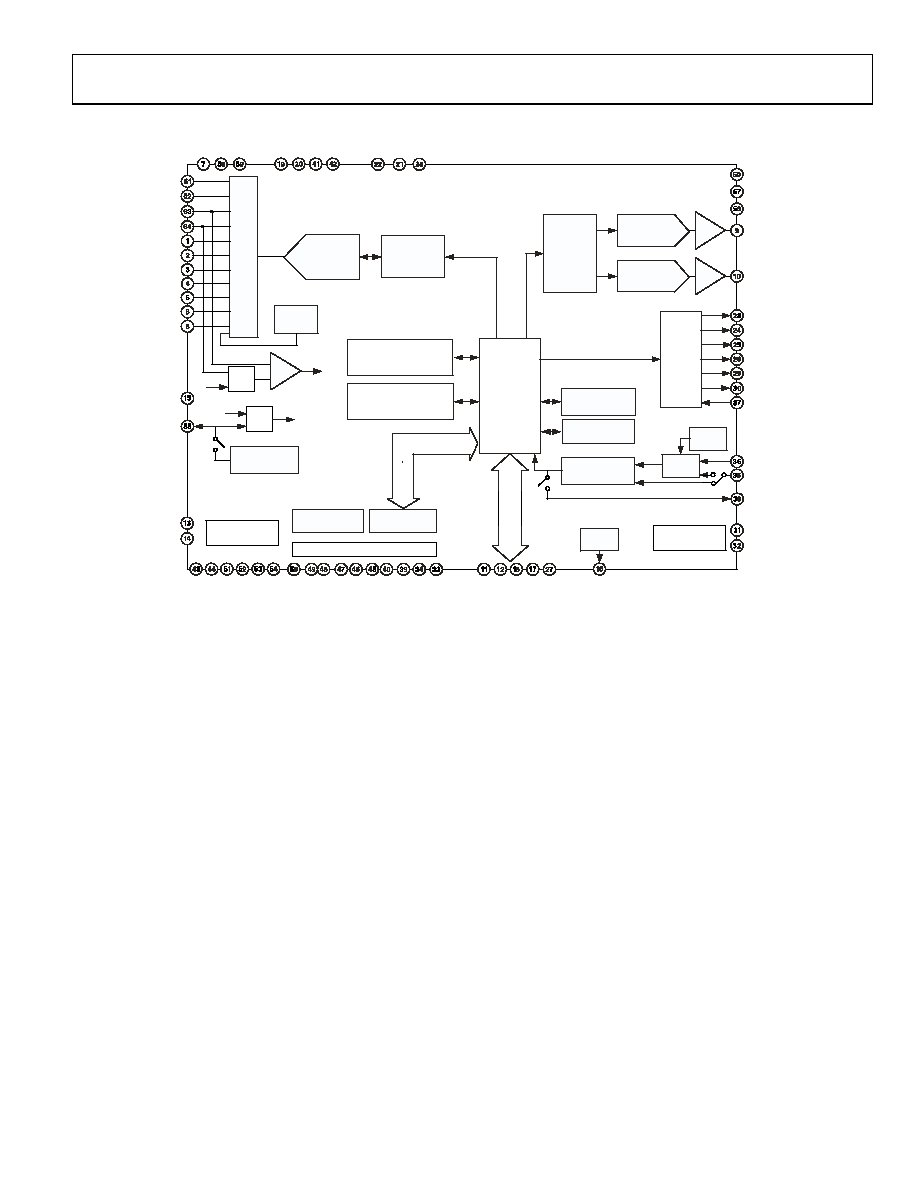
FUNCTIONAL BLOCK DIAGRAM
1MSPS
12-BIT ADC
ADC0
+
-
CMP0
CMP1
CMP
OUT
ADC7
...
...
V
REF
ADC9
ARM7TDMI-BASED MCU WITH
ADDITIONAL PERIPHERALS
2kX32 SRAM
31kX16 FLASH/EEPROM
GPIO
JTAG
4 GEN. PUR-
POSE TIMERS
SERIAL I/O
UART, SPI, 2xI2C
PLA
RST
ADuC7024
ADC8
MUX
BANDGAP
REF
TEMP
SENSOR
POR
OSC
& PLL
PSM
PWM0L
PWM0H
PWM1H
PWM1L
PWM2H
PWM2L
Three-
phase
PWM
DAC0
12-BIT DAC
DAC1
12-BIT DAC
XCLKI
XCLKO
Figure 1
Rev. PrC
Information furnished by Analog Devices is believed to be accurate and reliable.
However, no responsibility is assumed by Analog Devices for its use, nor for any
infringements of patents or other rights of third parties that may result from its use.
Specifications subject to change without notice. No license is granted by implication
or otherwise under any patent or patent rights of Analog Devices. Trademarks and
registered trademarks are the property of their respective companies.
One Technology Way, P.O. Box 9106, Norwood, MA 02062-9106, U.S.A.
Tel: 781.329.4700
www.analog.com
Fax: 781.326.8703
© 2004 Analog Devices, Inc. All rights reserved.

ADuC7024
Preliminary Technical Data
Rev. PrC | Page 2 of 18
TABLE OF CONTENTS
ADuC7024--Specifications ............................................................ 3
Terminology ...................................................................................... 6
Absolute Maximum Ratings............................................................ 7
Ordering Guide............................................................................. 7
Pin function descriptions ................................................................ 8
General Description ....................................................................... 12
Overview of the ARM7TDMI core.......................................... 12
Memory organisation ................................................................ 13
In-Circuit Serial Downloader................................................... 17
Outline Dimensions ....................................................................... 18

Preliminary Technical Data
ADuC7024
Rev. PrC | Page 3 of 18
ADUC7024--SPECIFICATIONS
1
Table 1. (AV
DD
= IOV
DD
= 2.7 to 3.6V, V
REF
= 2.5 V Internal Reference, f
CORE
= 45MHz, All specifications T
A
= T
MAX
to T
MIN
,
unless otherwise noted.)
Parameter
ADuC7024
Unit
Test Conditions/Comments
ADC CHANNEL SPECIFICATIONS
DC Accuracy
2, 3
f
SAMPLE
= 1MSPS
Resolution
12
Bits
Integral Nonlinearity
Integral Nonlinearity
4
±1.5
±0.5
±2.0
LSB max
LSB typ
LSB max
2.5V internal reference
2.5V internal reference
1.0V external reference
Differential Nonlinearity
Differential Nonlinearity
4
DC Code Distribution
+1/-0.9
±0.5
+1/-0.9
1
LSB max
LSB typ
LSB max
LSB typ
2.5V internal reference
2.5V internal reference
1.0V external reference
ADC input is a dc voltage
CALIBRATED ENDPOINT ERRORS
5
Offset Error
Offset Error Match
±5
±1
LSB max
LSB typ
Gain Error
Gain Error Match
±5
±1
LSB max
LSB typ
DYNAMIC PERFORMANCE
Fin = 10kHz Sine Wave, f
SAMPLE
= 1MSPS
Signal-to-Noise Ratio (SNR)
6
71
dB typ
Total Harmonic Distortion (THD)
-78
dB typ
Peak Harmonic or Spurious Noise
Channel-to-Channel Crosstalk
7
-78
-80
dB typ
dB typ
ANALOG INPUT
Input Voltage Ranges
Differential mode
V
CM
8
±V
REF
/2
Volts
Single-ended mode
0 to V
REF
Volts
Leakage Current
±5
µA max
Input Capacitance
20
pF typ
During ADC Acquisition
ON-CHIP VOLTAGE REFERENCE
Output Voltage
2.5
V
0.47µF from V
REF
(pin 55) to AGND
Accuracy
±10
mV max
Measured at T
A
= 25°C
Reference Temperature Coefficient
Power Supply Rejection Ratio
±10
80
ppm/°C typ
dB typ
Output Impedance
Internal V
REF
Power-On Time
10
1
typ
ms typ
EXTERNAL REFERENCE INPUT
9
Input Voltage Range
Input Impedance
0.625
AV
DD
TBD
V min
V max
K typ
DAC CHANNEL SPECIFICATIONS
R
L
= 5k
, C
L
= 100pF
DC ACCURACY
Resolution
12
Bits
Relative Accuracy
±2
LSB typ
Differential Nonlinearity
±1
LSB max
Guaranteed Monotonic
Offset Error
±2
±5
mV max
mV max
DAC output unbuffered
DAC output buffered
Gain Error
Gain Error Mismatch
±0.5
TBD
% max
% typ
% of fullscale on DAC0

ADuC7024
Preliminary Technical Data
Rev. PrC | Page 4 of 18
Parameter
ADuC7024
Unit
Test Conditions/Comments
ANALOG OUTPUTS
Output Voltage Range_0
Ouput Voltage Range_1
Output Voltage Range_2
0 to DACREF
0 to 2.5V
0 to DACV
DD
V typ
V typ
V typ
DACREF range: DACGND to DACV
DD
Output Impedance
10
typ
DAC AC CHARACTERISTICS
Voltage Output Settling Time
Voltage Output Settling Time
Digital to Analog Glitch Energy
10
15
TBD
µs typ
µs typ
nV-sec typ
DAC Output buffered
DAC Output unbuffered
I LSB change at major carry
COMPARATOR
Input Offset Voltage
Input Bias Current
Input Voltage Range
Input Capacitance
Hysteresis
Response Time
±10
5
AV
DD
-1.2
7
5
10
1
10
mV
nA typ
V max
pF typ
mV min
mv max
µs min
µs max
Hysteresis can be turned on or off via the CMPHYST
bit in the CMPCON register
Response time may be modified via the CMPRES bits
in the CMPCON register
TEMPERATURE SENSOR
Voltage Output at 25°C
Voltage TC
TBD
-2.0
mV typ
mV/°C typ
Accuracy
±3
°C typ
POWER SUPPLY MONITOR (PSM)
IOV
DD
Trip Point Selection
2.79
V
Two selectable Trip Points
3.07
V
Power Supply Trip Point Accuracy
±2.5
% max
Of the selected nominal Trip Point Voltage
Watchdog Timer (WDT)
4
Timeout Period
0
TBD
ms min
ms max
Flash/EE MEMORY
Endurance
10
10,000
Cycles min
Data Retention
11
30
Years min
T
J
= 55°C
Digital Inputs
Input Leakage Current
Input Capacitance
±10
±1
10
µA max
µA typ
pF typ
All digital inputs including XTAL1 and XTAL2
Logic Inputs
4
VINL, Input Low Voltage
VINH, Input High Voltage
0.4
2.0
V max
V min
All Logic inputs including XTAL1 and XTAL2
Logic Outputs
VOH, Output High Voltage
2.4
V min
I
SOURCE
= 20µA
VOL, Output Low Voltage
0.4
V max
I
SINK
= 1.6mA
MCU CLOCK RATE
355.5
45.5
kHz min
MHz max
8 programmable core clock selections within this
range
STARTUP TIME
At Power-On
From Idle Mode
From Power-Down Mode
TBD
TBD
TBD
Core Clock = TBD MHz
Programmable Logic Array (PLA)
Propagation Delay
TBD
ns typ
From input pin to output pin

Preliminary Technical Data
ADuC7024
Rev. PrC | Page 5 of 18
Parameter
ADuC7024
Unit
Test Conditions/Comments
POWER REQUIREMENTS
12
,
13
Power Supply Voltage Range
AV
DD
AGND and IOV
DD
- IOGND
2.7
V min
3.6
V max
Power Supply Current Normal Mode
3mA
5
50
mA typ
mA max
mA typ
1MHz clock
1MHz clock
45MHz clock
60
mA max
45MHz clock
Power Supply Current Idle Mode
Power Supply Current Power Down
Mode
1
30
100
mA max
µA typ
µA max
External Crystal or Internal Osc ON
External Crystal or Internal Osc ON
1
Temperature Range -40° to +85°C
2
All ADC Channel Specifications are guaranteed during normal MicroConverter core operation.
3
These specification apply to all ADC input channels.
4
These numbers are not production tested but are supported by design and/or characterization data on production release.
5
Based on external ADC system components, the user may need to execute a system calibration to remove external endpoint and achieve these specifications..
6
SNR calculation includes distortion and noise components.
7
Channel-to-channel crosstalk is measured on adjacent channels.
8
The input signal can be centered on any dc common-mode voltage (V
CM
) as long as this value is within the ADC voltage input range specified.
9
When using an external reference input pin, the internal reference must be disabled by setting the lsb in the REFCON Memeory Mapped Register to 0.
10
Endurance is qualified to 50,000 cycles as per JEDEC Std. 22 method A117 and measured at -40°C, +25°C and +85°C. Typical endurance at 25°C is 70,000 cycles.
11
Retention lifetime equivalent at junction temperature (Tj) = 55°C as per JEDEC Std. 22 method A117. Retention lifetime will derate with junction temperature.
12
Power supply current consumption is measured in normal, idle and power-down modes under the following conditions:
Normal Mode:
TBD
Idle Mode:
TBD
Power-Down:
TBD
13
DV
DD
power supply current increases typically by TBD mA during a Flash/EE memory program or erase cycle.

ADuC7024
Preliminary Technical Data
Rev. PrC | Page 6 of 18
TERMINOLOGY
ADC Specifications
Integral Nonlinearity
This is the maximum deviation of any code from a straight line
passing through the endpoints of the ADC transfer function.
The endpoints of the transfer function are zero scale, a point 1/2
LSB below the first code transition and full scale, a point 1/2
LSB above the last code transition.
Differential Nonlinearity
This is the difference between the measured and the ideal 1 LSB
change between any two adjacent codes in the ADC.
Offset Error
This is the deviation of the first code transition (0000 . . . 000) to
(0000 . . . 001) from the ideal, i.e., +1/2 LSB.
Gain Error
This is the deviation of the last code transition from the ideal
AIN voltage (Full Scale 1.5 LSB) after the offset error has been
adjusted out.
Signal to (Noise + Distortion) Ratio
This is the measured ratio of signal to (noise + distortion) at the
output of the ADC. The signal is the rms amplitude of the
fundamental. Noise is the rms sum of all nonfundamental
signals up to half the sampling frequency (fS/2), excluding dc.
The ratio is dependent upon the number of quantization levels
in the digitisation process; the more levels, the smaller the
quantization noise. The theoretical signal to (noise + distortion)
ratio for an ideal N-bit converter with a sine wave input is given
by:
Signal to (Noise + Distortion) = (6.02N + 1.76) dB
Thus for a 12-bit converter, this is 74 dB.
Total Harmonic Distortion
Total Harmonic Distortion is the ratio of the rms sum of the
harmonics to the fundamental.
DAC SPECIFICATIONS
Relative Accuracy
Relative accuracy or endpoint linearity is a measure of the
maximum deviation from a straight line passing through the
endpoints of the DAC transfer function. It is measured after
adjusting for zero error and full-scale error.
Voltage Output Settling Time
This is the amount of time it takes for the output to settle to
within a 1 LSB level for a full-scale input change..
Preliminary Technical Data
ADuC7024
Rev. PrC | Page 7 of 18
ABSOLUTE MAXIMUM RATINGS
Table 2. Absolute Maximum Ratings (T
A
= 25°C unless otherwise noted)
Parameter
Rating
AV
DD
to DV
DD
TBD
AGND to DGND
TBD
DV
DD
to DGND, AV
DD
to AGND
TBD
Digital Input Voltage to DGND
TBD
Digital Output Voltage to DGND
TBD
VREF to AGND
TBD
Analog Inputs to AGND
TBD
Operating Temperature Range
Industrial ADuC7024
40°C to +85°C
Storage Temperature Range
TBD
Junction Temperature
TBD
JA
Thermal Impedance
(ADuC7024BCP)
TBD
Lead Temperature, Soldering
Vapor Phase (60 sec)
TBD
Infrared (15 sec)
TBD
Stresses above those listed under Absolute M aximum Ratings
may cause permanent damage to the device. This is a stress
rating only; functional operation of the device at these or any
other conditions above those listed in the operational sections
of this specification is not implied. Exposure to absolute
maximum rating conditions for extended periods may affect
device reliability.
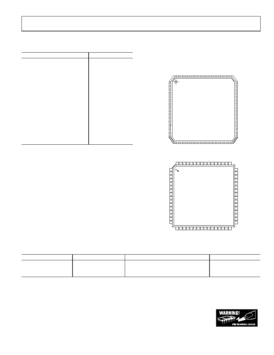
PIN CONFIGURATION
64-Lead CSP
33
32
49
48
16
17
PIN 1
IDENTIFIER
1
64
ADuC7024
TOP VIEW
(Not to Scale)
64-Lead LQFP
64
49
17
1
16
48
33
PIN 1
IDENTIFIER
TOP VIEW
(Not to Scale)
ADuC7024 64-LEAD LQFP
32
ORDERING GUIDE
Model
Temperature Range
Package Description
Package Option
ADuC7024BCP
40°C to + 85°C
64-Lead Chip Scale Package
CP-64
ADuC7024BST
40°C to + 85°C
Lead Plastic Quad Flatpack
ST-64
EVAL_ADuC7024QS
Development System
Contact the factory for chip availability.
ESD Caution
ESD (electrostatic discharge) sensitive device. Electrostatic charges as high as 4000 V readily accumulate on the
human body and test equipment and can discharge without detection. Although this product features
proprietary ESD protection circuitry, permanent damage may occur on devices subjected to high-energy
electrostatic discharges. Therefore, proper ESD precautions are recommended to avoid performance
degradation or loss of functionality.

ADuC7024
Preliminary Technical Data
Rev. PrC | Page 8 of 18
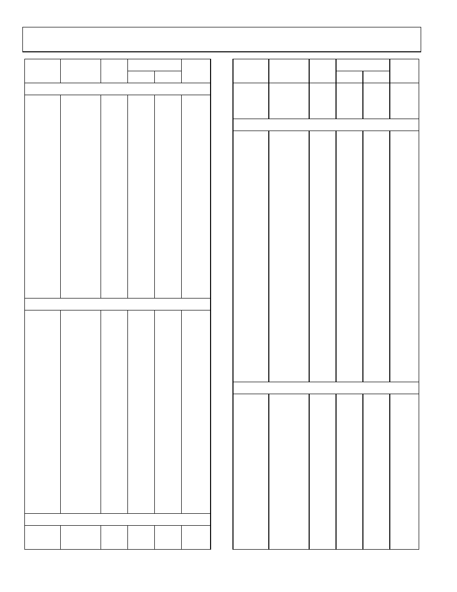
PIN FUNCTION DESCRIPTIONS
Table 3. Pin Function Descriptions
Pin#
Mnemonic
Type
*
Function
1
ADC4
I
Single-ended or differential Analog input 4
2
ADC5
I
Single-ended or differential Analog input 5
3
ADC6
I
Single-ended or differential Analog input 6
4
ADC7
I
Single-ended or differential Analog input 7
5
ADC8
I
Single-ended or differential Analog input 8
6
ADC9
I
Single-ended or differential Analog input 9
7
GND
REF
S
Ground voltage reference for the ADC. For optimal performance the analog
power supply should be separated from IOGND and DGND
8
ADCNEG
I
Bias point or Negative Analog Input of the ADC in pseudo differential mode.
Must be connected to the ground of the signal to convert. This bias point
must be between 0V and 1V
9
DAC0/ADC12
I/O
DAC0 Voltage Output / Single-ended or differential Analog input 12
10
DAC1/ADC13
I/O
DAC1 Voltage Output / Single-ended or differential Analog input 13
11
TMS
I
JTAG Test Port Input - Test Mode Select. Debug and download access
12
TDI
I
JTAG Test Port Input Test Data In. Debug and download access
13
P4.6/PLAO[14]
I/O
General Purpose Input-Output Port 4.6/ Programmable Logic Array Output
Element 14
14
P4.7/PLAO[15]
I/O
General Purpose Input-Output Port 4.7/ Programmable Logic Array Output
Element 15
15
BM/P0.0/CMP
OUT
/PLAI[7]
I/O
Multifunction I/O pin:
Boot Mode. The ADuC7024 will enter UART serial download mode if BM is low
at reset and will execute code if BM is pulled high at reset through a 1kOhm
resistor/ General Purpose Input-Output Port 0.0 / Voltage Comparator
Output/ Programmable Logic Array Input Element 7
16
P0.6/T1/MRST/PLAO[3]
O
Multifunction pin: driven low after reset
General Purpose Output Port 0.6 / Timer 1 Input / Power on reset output /
Programmable Logic Array Output Element 3
17
TCK
I
JTAG Test Port Input - Test Clock. Debug and download access
18
TDO
O
JTAG Test Port Output - Test Data Out. Debug and download access
19
IOGND
S
Ground for GPIO. Typically connected to DGND
20
IOV
DD
S
3.3V Supply for GPIO and input of the on-chip voltage regulator.
21
LV
DD
S
2.5V. Output of the on-chip voltage regulator. Must be connected to a 0.47
µ
F
capacitor to DGND
22
DGND
S
Ground for core logic.
23
P3.0/PWM0
H
/PLAI[8]
I/O
General Purpose Input-Output Port 3.0/ PWM phase 0 high side output /
Programmable Logic Array Input Element 8
24
P3.1/PWM0
L
/PLAI[9]
I/O
General Purpose Input-Output Port 3.1/ PWM phase 0 low side output /
Programmable Logic Array Input Element 9
25
P3.2/PWM1
H
/PLAI[10]
I/O
General Purpose Input-Output Port 3.2/ PWM phase 1 high side output /
Programmable Logic Array Input Element 10
26
P3.3/PWM1
L
/PLAI[11]
I/O
General Purpose Input-Output Port 3.3/ PWM phase 1 low side output /
Programmable Logic Array Input Element 11
27
P0.3/TRST/ADC
BUSY
I/O
General Purpose Input-Output Port 0.3 / JTAG Test Port Input Test Reset.
Debug and download access / ADC
BUSY
signal output
28
RST
I
Reset Input. (active low)
29
P3.4/PWM2
H
/PLAI[12]
I/O
General Purpose Input-Output Port 3.4 / PWM phase 2 high side output /
Programmable Logic Array Input 12
30
P3.5/PWM2
L
/PLAI[13]
I/O
General Purpose Input-Output Port 3.5 / PWM phase 2 low side output /
Programmable Logic Array Input Element 13
Preliminary Technical Data
ADuC7024
Rev. PrC | Page 9 of 18
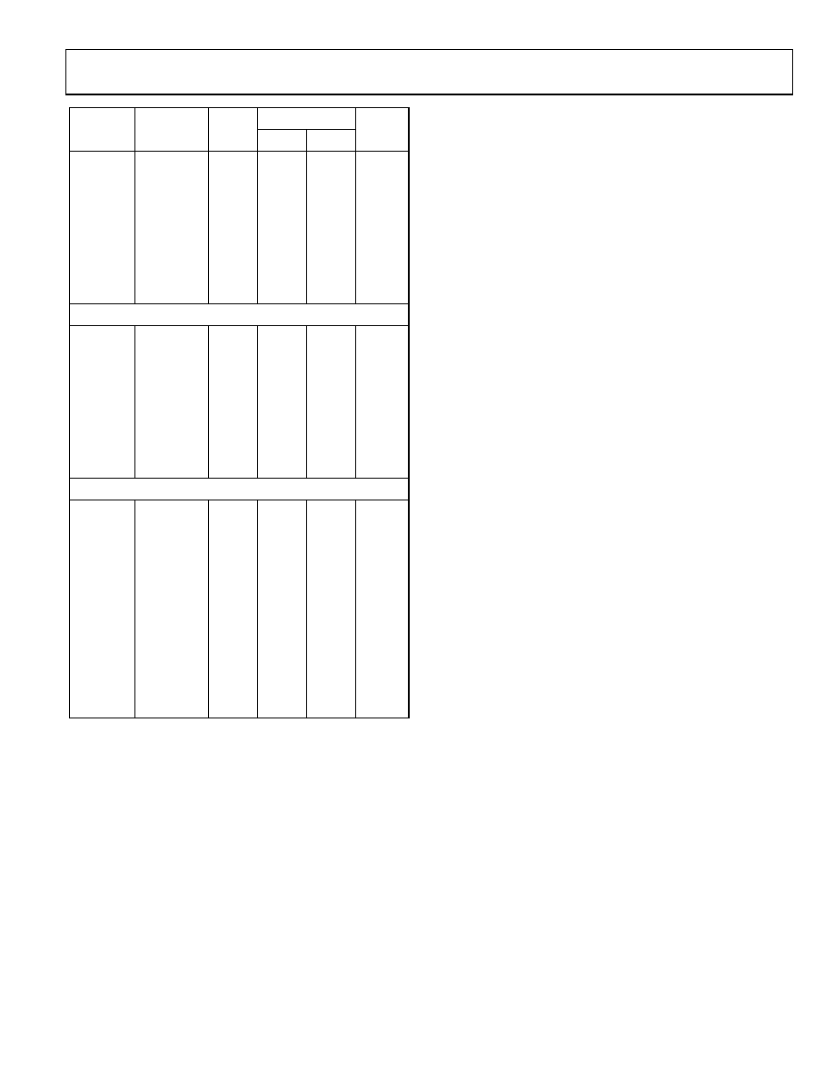
Pin#
Mnemonic
Type
*
Function
31
IRQ0/P0.4/CONV
START
/PLAO[1]
I/O
Multifunction I/O pin:
External Interrupt Request 0, active high / General Purpose Input-Output Port
0.4 / Start conversion input signal for ADC / Programmable Logic Array
Output Element 1
32
IRQ1/P0.5/ADC
BUSY
/PLAO[2]
I/O
Multifunction I/O pin:
External Interrupt Request 1, active high / General Purpose Input-Output Port
0.5 / ADC
BUSY
signal / Programmable Logic Array Output Element 2
33
P2.0/PWM
TRIP
/SPM9/PLAO[5]/CONV
START
I/O
Serial Port Multiplexed:
General Purpose Input-Output Port 2.0 / PWM safety cut off / UART /
Programmable Logic Array Output Element 5/ Start conversion input signal
for ADC
34
P0.7/ECLK/SPM8/PLAO[4]
I/O
Serial Port Multiplexed:
General Purpose Input-Output Port 0.7 / Output for External Clock signal /
UART / Programmable Logic Array Output Element 4
35
XCLKO
O
Output to the crystal oscillator inverter
36
XCLKI
I
Input to the crystal oscillator inverter and input to the internal clock
generator circuits
37
P3.6/PWM
TRIP
/PLAI[14]
I/O
General Purpose Input-Output Port 3.6/ PWM safety cut off / Programmable
Logic Array Input Element 14
38
P3.7/ECLK/PLAI[15]
I/O
General Purpose Input-Output Port 3.7/ Output for External Clock signal
/Programmable Logic Array Input Element 15
39
P1.7/SPM7/PLAO[0]
I/O
Serial Port Multiplexed:
General Purpose Input-Output Port 1.7 / UART / SPI / Programmable Logic
Array Output Element 0
40
P1.6/SPM6/PLAI[6]
I/O
Serial Port Multiplexed:
General Purpose Input-Output Port 1.6 / UART / SPI / Programmable Logic
Array Input Element 6
41
IOGND
S
Ground for GPIO. Typically connected to DGND
42
IOV
DD
S
3.3V Supply for GPIO and input of the on-chip voltage regulator.
43
P4.0/PLAO[8]
I/O
General Purpose Input-Output Port 4.0 / Programmable Logic Array Output
Element 8
44
P4.1/PLAO[9]
I/O
General Purpose Input-Output Port 4.1 / Programmable Logic Array Output
Element 9
45
P1.5/SPM5/PLAI[5]
I/O
Serial Port Multiplexed:
General Purpose Input-Output Port 1.5 / UART / SPI / Programmable Logic
Array Input Element 5
46
P1.4/SPM4/PLAI[4]
I/O
Serial Port Multiplexed:
General Purpose Input-Output Port 1.4 / UART / SPI / Programmable Logic
Array Input Element 4
47
P1.3/SPM3/PLAI[3]
I/O
Serial Port Multiplexed:
General Purpose Input-Output Port 1.3/ UART / I
2
C1 /Programmable Logic
Array Input Element 3
48
P1.2/SPM2/PLAI[2]
I/O
Serial Port Multiplexed:
General Purpose Input-Output Port 1.2 / UART / I
2
C1 /Programmable Logic
Array Input Element 2
49
P1.1/SPM1/PLAI[1]
I/O
Serial Port Multiplexed:
General Purpose Input-Output Port 1.1 / UART / I
2
C0 / Programmable Logic
Array Input Element 1
50
P1.0/T1/SPM0/PLAI[0]
I/O
Serial Port Multiplexed:
General Purpose Input-Output Port 1.0/ Timer 1 Input / UART / I
2
C0 /
Programmable Logic Array Input Element 0
51
P4.2/PLAO[10]
I/O
General Purpose Input-Output Port 4.2 / Programmable Logic Array Output
Element 10
ADuC7024
Preliminary Technical Data
Rev. PrC | Page 10 of 18
Pin#
Mnemonic
Type
*
Function
52
P4.3/PLAO[11]
I/O
General Purpose Input-Output Port 4.3 / Programmable Logic Array Output
Element 11
53
P4.4/PLAO[12]
I/O
General Purpose Input-Output Port 4.4 / Programmable Logic Array Output
Element 12
54
P4.5/PLAO[13]
I/O
General Purpose Input-Output Port 4.5 / Programmable Logic Array Output
Element 13
55
V
REF
I/O
2.5V internal Voltage Reference. Must be connected to a 0.47uF capacitor
when using the internal reference.
56
DAC
REF
I
External Voltage Reference for the DACs. Range: DACGND to DACV
DD
57
DACGND
S
Ground for the DAC. Typically connected to AGND
58
AGND
S
Analog Ground. Ground reference point for the analog circuitry
59
AV
DD
S
3.3V Analog Power
60
DACV
DD
S
3.3V Power Supply for the DACs. Typically connected to AV
DD
61
ADC0
I
Single-ended or differential Analog input 0
62
ADC1
I
Single-ended or differential Analog input 1
63
ADC2/CMP0
I
Single-ended or differential Analog input 2/ Comparator positive input
64
ADC3/CMP1
I
Single-ended or differential Analog input 3/ Comparator negative input
*
I = Input, O = Output, S = Supply.
Preliminary Technical Data
ADuC7024
Rev. PrC | Page 11 of 18
P
1
.
7
/
S
P
M
7
/
P
L
A
I
P
1
.
6
/
S
P
M
6
/
P
L
A
I
P
1
.
5
/
S
P
M
5
/
P
L
A
I
P
1
.
4
/
S
P
M
4
/
P
L
A
I
P
1
.
3
/
S
P
M
3
/
P
L
A
I
P
1
.
2
/
S
P
M
2
/
P
L
A
I
P
1
.
1
/
S
P
M
1
/
P
L
A
I
P
1
.
0
/
S
P
M
0
/
P
L
A
I
P
0
.
7
/
E
C
L
K
/
S
P
M
8
/
P
L
A
O
P
2
.
0
/
P
W
M
T
R
I
P
/
S
P
M
9
/
P
L
A
O
/
C
O
M
V
S
T
A
R
T
T
C
K
/
X
C
L
K
P
0
.
3
/
T
R
S
T
/
A
D
C
B
U
S
Y
T
D
O
T
D
I
T
M
S
UART
SERIAL PORT
SPI/I
2
C SERIAL
INTERFACE
SERIAL PORT MULTIPLEXER
IRQ1/P0.5/ADC
BUSY
/PLAO
IRQ0/P0.4/CONV
START
/PLAO
OSC
PROG. CLOCK
DIVIDER
XCLKO
XCLKI
PLL
PROG. LOGIC
ARRAY
INTERRUPT
CONTROLLER
P4.6/PLAO
P4.7/PLAO
P
4
.
0
/
P
L
A
O
P
4
.
2
/
P
L
A
O
P
4
.
3
/
P
L
A
O
P
4
.
1
/
P
L
A
O
P
4
.
5
/
P
L
A
O
P
4
.
4
/
P
L
A
O
POR
P
0
.
6
/
M
R
S
T
/
P
L
A
O
J
T
A
G
E
M
U
L
A
T
O
R
8192 BYTES USER RAM
(2k X 32 bits)
POWER SUPPLY
MONITOR
ARM7TDMI
MCU
CORE
62 KBYTES FLASH/EE
(31k X 16 bits)
DOWNLOADER
V
REF
MUX
DAC
V
REF
BAND GAP
REFERENCE
WAKEUP/
RTC TIMER
R
E
S
E
T
ADC0
TEMP
SENSOR
ADC1
MUX
12-BIT SAR
ADC 1MSPS
ADC
CONTROL
G
N
D
R
E
F
A
G
N
D
I
O
G
N
D
I
O
V
D
D
D
G
N
D
A
V
D
D
DACV
DD
ADuC7024
DAC0/ADC12
BUF
12-BIT
VOLTAGE
OUTPUT DAC
DAC1/ADC13
BUF
12-BIT
VOLTAGE
OUTPUT DAC
DAC
CONTROL
P3.6/PWM
TRIP
/PLAI
P3.5/PWM2H/PLAI
P3.4/PWM2H/PLAI
P3.3/PWM1H/PLAI
P3.2/PWM1H/PLAI
P3.1/PWM0L/PLAI
P3.0/PWM0H/PLAI
Three-
phase
PWM
L
V
D
D
DAC
REF
DACGND
ADC2/CMP0
ADC8
ADC4
ADC3/CMP1
ADC9
ADC
NEG
MUX
DAC
CMP
OUT
/IRQ
BM/P0.0/CMP
OUT
/PLAO
ADC7
ADC6
ADC5
P3.7/ECLK/PLAI
I
O
G
N
D
I
O
V
D
D
Figure 2: Detailed Block Diagram

ADuC7024
Preliminary Technical Data
Rev. PrC | Page 12 of 18
GENERAL DESCRIPTION
The ADuC7024 is fully integrated, 1MSPS, 12-bit data
acquisition system incorporating a high performance multi-
channel ADC, a 16/32-bit M CU and Flash/EE M emory on a
single chip.
The ADC consists of 10 single-ended inputs. An additional 2
inputs are available but are multiplexed with the 2 DAC output
pins. The ADC can operate in single-ended or differential input
modes. The ADC input voltage is 0 to V
REF
. Low drift bandgap
reference, temperature sensor and voltage comparator complete
the ADC peripheral set.
The part also integrates 2 buffered voltage output DACs on-
chip. The DAC output range is programmable to one of three
voltage ranges.
The device operates from an on-chip oscillator and PLL
generating an internal high-frequency clock of 45 MHz. This
clock is routed through a programmable clock divider from
which the MCU core clock operating frequency is generated.
The microcontroller core is an ARM7TDMI, 16/32-bit RISC
machine, offering up to 45 M IPS peak performance. 62k Bytes
of non-volatile Flash/EE are provided on-chip as well as 8k
Bytes of SRAM. Both the Flash/EE and SRAM memory arrays
are mapped into a single linear array.
On-chip factory firmware supports in-circuit serial download
via the UART and JTAG serial interface ports while non-
intrusive emulation is also supported via the JTAG interface.
These features are incorporated into a low-cost QuickStart
Development System supporting this MicroConverter family.
The parts operate from 2.7V to 3.6V and are specified over an
industrial temperature range of -40°C to 85°C. When operating
at 45MHz the power dissipation is 300mW. The ADuC7024 is
available in a 64-lead LFCSP package and 64-lead LQFP.
OVERVIEW OF THE ARM7TDMI CORE
The ARM7 core is a 32-bit Reduced Instruction Set Computer
(RISC). It uses a single 32-bit bus for instruction and data. The
length of the data can be 8, 16 or 32 bits and the length of the
instruction word is 32 bits.
The ARM7TDMI is an ARM7 core with 4 additional features:
- T support for the Thumb (16 bit) instruction set.
- D support for debug
- M support for long multiplies
- I include the EmbeddedICE module to support embedded
system debugging.
Thumb mode (T)
An ARM instruction is 32-bits long. The ARM7TDMI
processor supports a second instruction set that has been
compressed into 16-bits, the Thumb instruction set. Faster
execution from 16-bit memory and greater code density can
usually be achieved by using the Thumb instruction set instead
of the ARM instruction set, which makes the ARM7TDMI core
particularly suitable for embedded applications.
However the Thumb mode has two limitations:
- Thumb code usually uses more instructions for the same job,
so ARM code is usually best for maximising the performance
of the time-critical code.
- The Thumb instruction set does not include some
instructions that are needed for exception handling, so ARM
code needs to be used for exception handling.
See ARM7TDMI User Guide for details on the core
architecture, the programming model and both the ARM and
ARM Thumb instruction sets.
Long multiple (M)
The ARM7TDMI instruction set includes four extra
instructions which perform 32-bit by 32-bit multiplication with
64-bit result and 32-bit by 32-bit multiplication-accumulation
(MAC) with 64-bit result.
EmbeddedICE (I)
EmbeddedICE provides integrated on-chip support for the core.
The EmbeddedICE module contains the breakpoint and
watchpoint registers which allow code to be halted for
debugging purposes. These registers are controlled through the
JTAG test port.
When a breakpoint or watchpoint is encountered, the processor
halts and enters debug state. Once in a debug state, the
processor registers may be inspected as well as the Flash/EE, the
SRAM and the Memory Mapped Registers.
Exceptions
ARM supports five types of exceptions, and a privileged
processing mode for each type. The five type of exceptions are:
- Normal interrupt or IRQ. It is provided to service general-
purpose interrupt handling of internal and external events
- Fast interrupt or FIQ. It is provided to service data transfer or
communication channel with low latency. FIQ has priority
over IRQ
- Memory abort
- Attempted execution of an undefined instruction
- Software interrupt (SWI) instruction which can be used to
make a call to an operating system.
Typically the programmer will define interrupts as IRQ but for
higher priority interrupt, i.e. faster response time, the
programmer can define interrupt as FIQ.
Preliminary Technical Data
ADuC7024
Rev. PrC | Page 13 of 18
ARM Registers
ARM7TDMI has a total of 37 registers, of which 31 are general
purpose registers and six are status registers. Each operating
mode has dedicated banked registers.
When writing user-level programs, 15 general purpose 32-bit
registers (r0 to r14), the program counter (r15) and the current
program status register (CPSR) are usable. The remaining
registers are used only for system-level programming and for
exception handling.
When an exception occurs, some of the standard register are
replaced with registers specific to the exception mode. All
exception modes have replacement banked registers for the
stack pointer (r13) and the link register (r14) as represented in
Figure 3. The fast interrupt mode has more registers (8 to 12)
for fast interrupt processing, so that the interrupt processing
can begin without the need to save or restore these registers and
thus save critical time in the interrupt handling process.
Figure 3: register organisation
Interrupt latency
The worst case latency for an FIQ, assuming that it is enabled,
consists of the longest time the request can take to pass through
the synchronizer, plus the time for the longest instruction to
complete (the longest instruction is an LDM) which loads all
the registers including the PC, plus the time for the data abort
entry, plus the time for FIQ entry. At the end of this time, the
ARM 7TDM I will be executing the instruction at 0x1C (FIQ
interrupt vector address). The maximum total time is 44
processor cycles, which is just over 975 nanoseconds in a system
using a continuous 45 MHz processor clock.
The maximum IRQ latency calculation is similar, but must
allow for the fact that FIQ has higher priority and could delay
entry into the IRQ handling routine for an arbitrary length of
time.
The minimum latency for FIQ or IRQ interrupts is four cycles
in total which consists of the shortest time the request can take
through the synchronizer plus the time to enter the exception
mode.
Note that the ARM7TDMI will always be run in ARM (32-bit)
mode when in privileged modes, i.e. when executing interrupt
service routines.
MEMORY ORGANISATION
The ADuC7024 incorporates two separate blocks of memory,
8kByte of SRAM and 64kByte of On-Chip Flash/EE memory.
62kByte of On-Chip Flash/EE memory are available to the user,
and the remaining 2kBytes are reserved for the factory
configured boot page. These two blocks are mapped as shown
Figure 4.
Note that by default, after a reset, the Flash/EE memory is
mirrored at address 0x00000000. It is possible to remap the
SRAM at address 0x00000000 by clearing bit 0 of the REMAP
MMR. This remap function is described in more details in the
Flash/EE memory chapter.
Re-mappable Memory Space
(Flash/EE or SRAM)
Reserved
00080000h
Flash/EE
Reserved
00011FFFh
00010000h
SRAM
FFFF0000h
FFFFFFFFh
MMRs
0000FFFFh
00000000h
0008FFFFh
Figure 4: Physical memory map
Memory Access
The ARM 7 core sees memory as a linear array of 232 byte
location where the different blocks of memory are mapped as
outlined in Figure 4 above.
The ADuC7024 memory organisation is configured in little
endian format: the least significant byte is located in the lowest
byte address and the most significant byte in the highest byte
address.
user mode
fiq
mode
svc
mode
abord
mode
irq
mode
undefined
mode
r0
r1
r2
r3
r4
r5
r6
r7
r8
r9
r10
r11
r12
r13
r14
r15 (PC)
r8_fiq
r9_fiq
r10_fiq
r11_fiq
r12_fiq
r13_fiq
r14_fiq
r13_svc
r14_svc
r13_abt
r14_abt
r13_irq
r14_irq
r13_und
r14_und
usable in user mode
system modes only
CPSR
SPSR_fiq
SPSR_svc
SPSR_und
SPSR_abt
SPSR_irq
ADuC7024
Preliminary Technical Data
Rev. PrC | Page 14 of 18
Figure 5: little endian format
Flash/EE Memory
The total 64kBytes of Flash/EE are organised as 32k X 16 bits.
31k X 16 bits are user space and 1k X 16 bits is reserved for boot
loader. The page size of this Flash/EE memory is 256Bytes.
62kBytes of Flash/EE are available to the user as code and non-
volatile data memory. There is no distinction between data and
program as ARM code shares the same space. The real width of
the Flash/EE memory is 16 bits, which means that in ARM
mode (32-bit instruction), two accesses to the Flash/EE are
necessary for each instruction fetch. It is therefore
recommended to use Thumb mode when executing from
Flash/EE memory for optimum access speed. The maximum
access speed for the Flash/EE memory is 45M Hz in Thumb
mode and 22.5M Hz in full ARM mode. M ore details on
Flash/EE access time are outlined later in `Execution from
SRAM and Flash/EE' section of this datasheet.
SRAM
8kBytes of SRAM are available to the user, organized as 2k X 32
bits, i.e. 2kWords. ARM code can run directly from SRAM at
45M Hz , given that the SRAM array is configured as a 32-bit
wide memory array. M ore details on SRAM access time are
outlined later in `Execution from SRAM and Flash/EE' section
of this datasheet.
Memory Mapped Registers
The Memory Mapped Register (MMR) space is mapped into
the upper 2 pages of the Flash/EE space and accessed by
indirect addressing through the ARM7 banked registers.
The MMR space provides an interface between the CPU and all
on-chip peripherals. All registers except the core registers
reside in the MMR area. All shaded locations shown in Figure 6
are unoccupied or reserved locations and should not be
accessed by user software. Table 4 shows a full MMR memory
map. The `Access' column corresponds to the access time
reading or writing a MMR. Table 4 shows a full MMR memory
map.
Interrupt
Controller
Remap &
System Control
I
2
C0
UART
DAC
ADC
PLA
Bandgap
Reference
Power Supply
Monitor
GPIO
Timer 0
PLL &
Oscillator Control
Watchdog
Timer
Flash Control
Interface
General Purpose
Timer
Wake Up
Timer
0xFFFF0000
0xFFFF0110
0xFFFF0320
0xFFFF0310
0xFFFF0300
0xFFFF0238
0xFFFF0220
0xFFFF0600
0xFFFFF400
0xFFFF0B54
0xFFFF0B00
0xFFFF0A14
0xFFFF0A00
0xFFFF0848
0xFFFF0800
0xFFFF0730
0xFFFF0700
0xFFFF0620
0xFFFF0500
0xFFFF0538
0xFFFF0490
0xFFFF048C
0xFFFF0334
0xFFFF0448
0xFFFF0440
0xFFFF0420
0xFFFF0404
0xFFFF0340
0xFFFF0350
0xFFFF0360
0xFFFF0370
0xFFFFF46C
0xFFFFFFFF
0xFFFFF800
0xFFFFF820
PWM
0xFFFFFC3C
0xFFFFFC00
I
2
C1
0xFFFF0948
0xFFFF0900
SPI
Figure 6: Memory Mapped
32 bits
Byte0
Byte1
Byte2
Byte3
0x00000000h
0x00000004h
bit0
bit31
0
1
2
3
4
5
6
7
8
9
A
B
..
.
...
...
..
.
0xFFFFFFFFh
Preliminary Technical Data
ADuC7024
Rev. PrC | Page 15 of 18
Table 4. Complete MMRs list
Access
Address
Name
Byte
Type
Cycle
Page
IRQ address base = 0xFFFF0000
0x0000
IRQSTA
4
R
1
0x0004
IRQSIG
4
R
1
0x0008
IRQEN
4
RW
1
0x000C
IRQCLR
4
W
1
0x0010
SWICFG
4
W
1
0x0100
FIQSTA
4
R
1
0x0104
FIQSIG
4
R
1
0x0108
FIQEN
4
RW
1
0x010C
FIQCLR
4
W
1
System Control address base = 0xFFFF0200
0x0220
REMAP
1
RW
1
0x0230
RSTSTA
1
R
1
0x0234
RSTCLR
1
W
1
Timer address base = 0xFFFF0300
0x0300
T0LD
2
RW
2
0x0304
T0VAL
2
R
2
0x0308
T0CON
2
RW
2
0x030C
T0CLRI
1
W
2
0x0320
T1LD
4
RW
2
0x0324
T1VAL
4
R
2
0x0328
T1CON
2
RW
2
0x032C
T1CLRI
1
W
2
0x0330
T1CAP
4
RW
2
0x0340
T2LD
4
RW
2
0x0344
T2VAL
4
R
2
0x0348
T2CON
2
RW
2
0x034C
T2CLRI
1
W
2
0x0360
T3LD
2
RW
2
0x0364
T3VAL
2
R
2
0x0368
T3CON
2
RW
2
0x036C
T3CLRI
1
W
2
PLL base address = 0xFFFF0400
0x0404
POWKY1
1
W
2
0x0408
POWCON
1
RW
2
0x040C
POWKY2
1
W
2
0x0410
PLLKY1
1
W
2
Access
Address
Name
Byte
Type
Cycle
Page
0x0414
PLLCON
1
RW
2
0x0418
PLLKY2
1
W
2
PSM address base = 0xFFFF0440
0x0440
PSMCON
2
RW
2
0x0444
CMPCON
2
RW
2
Reference address base = 0xFFFF0480
0x048C
REFCON
1
RW
2
ADC address base = 0xFFFF0500
0x0500
ADCCON
1
RW
2
0x0504
ADCCP
1
RW
2
0x0508
ADCCN
1
RW
2
0x050C
ADCSTA
1
RW
2
0x0510
ADCDAT
4
R
2
0x0514
ADCRST
1
RW
2
0x0530
ADCGN
2
RW
2
0x0534
ADCOF
2
RW
2
DAC address base = 0xFFFF0600
0x0600
DAC0CON
1
RW
2
0x0604
DAC0DAT
4
RW
2
0x0608
DAC1CON
1
RW
2
0x060C
DAC1DAT
4
RW
2
UART base address = 0xFFFF0700
0x0700
COMTX
1
RW
2
COMRX
1
R
2
COMDIV0
1
RW
2
0x0704
COMIEN0
1
RW
2
COMDIV1
1
R/W
2
0x0708
COMIID0
1
R
2
0x070C
COMCON0
1
RW
2
0x0710
COMCON1
1
RW
2
0x0714
COMSTA0
1
R
2
0x0718
COMSTA1
1
R
2
0x071C
COMSCR
1
RW
2
0x0720
COMIEN1
1
RW
2
0x0724
COMIID1
1
R
2
0x0728
COMADR
1
RW
2
0X072C
COMDIV2
2
RW
2
ADuC7024
Preliminary Technical Data
Rev. PrC | Page 16 of 18
Access
Address
Name
Byte
Type
Cycle
Page
I2C0 base address = 0xFFFF0800
0x0800
I2C0MSTA
1
R
2
0x0804
I2C0SSTA
1
R
2
0x0808
I2C0SRX
1
R
2
0x080C
I2C0STX
1
W
2
0x0810
I2C0MRX
1
R
2
0x0814
I2C0MTX
1
W
2
0x0818
I2C0CNT
1
RW
2
0x081C
I2C0ADR
1
RW
2
0x0824
I2C0BYTE
1
RW
2
0x0828
I2C0ALT
1
RW
2
0x082C
I2C0CFG
1
RW
2
0x0830
I2C0DIVH
1
RW
2
0x0834
I2C0DIVL
1
RW
2
0x0838
I2C0ID0
1
RW
2
0x083C
I2C0ID1
1
RW
2
0x0840
I2C0ID2
1
RW
2
0x0844
I2C0ID3
1
RW
2
I2C1 base address = 0xFFFF0900
0x0900
I2C1MSTA
1
R
2
0x0904
I2C1SSTA
1
R
2
0x0908
I2C1SRX
1
R
2
0x090C
I2C1STX
1
W
2
0x0910
I2C1MRX
1
R
2
0x0914
I2C1MTX
1
W
2
0x0918
I2C1CNT
1
RW
2
0x091C
I2C1ADR
1
RW
2
0x0924
I2C1BYTE
1
RW
2
0x0928
I2C1ALT
1
RW
2
0x092C
I2C1CFG
1
RW
2
0x0930
I2C1DIVH
1
RW
2
0x0934
I2C1DIVL
1
RW
2
0x0938
I2C1ID0
1
RW
2
0x093C
I2C1ID1
1
RW
2
0x0940
I2C1ID2
1
RW
2
0x0944
I2C1ID3
1
RW
2
SPI base address = 0xFFFF0A00
0x0A00
SPISTA
1
R
2
0x0A04
SPIRX
1
R
2
Access
Address
Name
Byte
Type
Cycle
Page
0x0A08
SPITX
1
W
2
0x0A0C
SPIDIV
1
RW
2
0x0A10
SPICON
2
RW
2
PLA base address = 0xFFFF0B00
0x0B00
PLAELM0
2
RW
2
0x0B04
PLAELM1
2
RW
2
0x0B08
PLAELM2
2
RW
2
0x0B0C
PLAELM3
2
RW
2
0x0B10
PLAELM4
2
RW
2
0x0B14
PLAELM5
2
RW
2
0x0B18
PLAELM6
2
RW
2
0x0B1C
PLAELM7
2
RW
2
0x0B20
PLAELM8
2
RW
2
0x0B24
PLAELM9
2
RW
2
0x0B28
PLAELM10
2
RW
2
0x0B2C
PLAELM11
2
RW
2
0x0B30
PLAELM12
2
RW
2
0x0B34
PLAELM13
2
RW
2
0x0B38
PLAELM14
2
RW
2
0x0B3C
PLAELM15
2
RW
2
0x0B40
PLACLK
1
RW
2
0x0B44
PLAIRQ
4
RW
2
0x0B48
PLAADC
4
RW
2
0x0B4C
PLADIN
4
R
2
0x0B50
PLADOUT
4
RW
2
GPIO base address = 0xFFFFF400
0xF400
GP0CON
4
RW
1
0xF404
GP1CON
4
RW
1
0xF408
GP2CON
4
RW
1
0xF40C
GP3CON
4
RW
1
0xF410
GP4CON
4
RW
1
0xF420
GP0DAT
4
RW
1
0xF424
GP0SET
1
W
1
0xF428
GP0CLR
1
W
1
0xF430
GP1DAT
4
RW
1
0xF434
GP1SET
1
W
1
0xF438
GP1CLR
1
W
1
0xF440
GP2DAT
4
RW
1
0xF444
GP2SET
1
W
1
Preliminary Technical Data
ADuC7024
Rev. PrC | Page 17 of 18
Access
Address
Name
Byte
Type
Cycle
Page
0xF448
GP2CLR
1
W
1
0xF450
GP3DAT
4
RW
1
0xF454
GP3SET
1
W
1
0xF458
GP3CLR
1
W
1
0xF460
GP4DAT
4
RW
1
0xF464
GP4SET
1
W
1
0xF468
GP4CLR
1
W
1
Flash/EE base address = 0xFFFFF800
0xF800
FEESTA
1
R
1
0xF804
FEEMOD
1
RW
1
0xF808
FEECON
1
RW
1
0xF80C
FEEDAT
2
RW
1
0xF810
FEEADR
2
RW
1
0xF818
FEESIGN
3
R
1
0xF81C
FEEPRO
4
RW
1
PWM base address= 0xFFFFFC00
0xFC00
PWMCON
2
RW
1
0xFC04
PWMSTA
2
RW
1
0xFC08
PWMDAT0
2
RW
1
0xFC0C
PWMDAT1
2
RW
1
0xFC10
PWMCFG
2
RW
1
0xFC14
PWMCH0
2
RW
1
0xFC18
PWMCH1
2
RW
1
0xFC1C
PWMCH2
2
RW
1
0xFC20
PWMEN
2
RW
1
0xFC24
PWMDAT2
2
RW
1
The `Access' column corresponds to the access time reading or
writing a M M R. It depends on the AM BA (Advanced
Microcontroller Bus Architecture) bus used to access the
peripheral. The processor has two AMBA busses, AHB
(Advanced High-performance Bus) used for system modules
and APB (Advanced Peripheral Bus) used for lower
performance peripheral.
Development Tools
An entry level, low cost development system is available for the
ADuC702X family. This system consists of the following PC-
based (Windows® compatible) hardware and software
development tools:
Hardware:
- ADuC702X Evaluation board
- Serial Port programming cable
- JTAG emulator
Software:
- Integrated Development Environment, incorporating
assembler, compiler and non intrusive JTAG-based
debugger
- Serial Downloader software
- Example Code
Miscellaneous:
- CD-ROM Documentation
IN-CIRCUIT SERIAL DOWNLOADER
The Serial Downloader is a Windows application that allows
the user to serially download an assembled program (Intel Hex
format file) to the on-chip program FLASH/EE memory via the
serial port on a standard PC.
ADuC7024
Preliminary Technical Data
Rev. PrC | Page 18 of 18
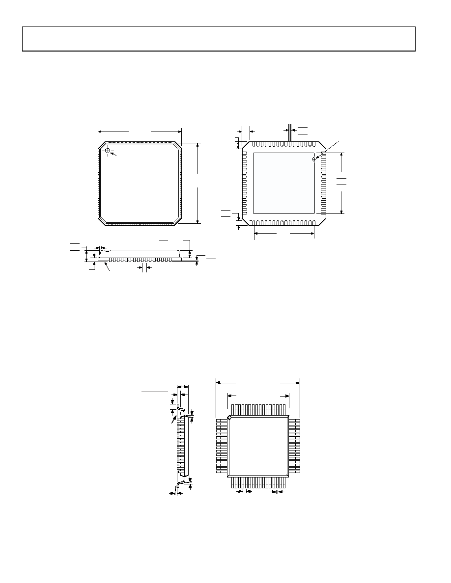
OUTLINE DIMENSIONS
PIN 1
INDICATOR
TOP
VIEW
8.75
BSC SQ
9.00
BSC SQ
1
64
16
17
49
48
32
33
BOTTOM
VIEW
0.45
0.40
0.35
0.30
0.25
0.18
0.50 BSC
12 MAX
0.20
REF
0.80 MAX
0.65 NOM
1.00
0.90
0.80
7.63
REF
SEATING
PLANE
0.05 MAX
0.02 NOM
0.60 MAX
0.60 MAX
PIN 1
INDICATOR
COMPLIANT TO JEDEC STANDARDS MO-220-VMMD
7.80
7.65
7.50
SQ
Figure 77. 64-Lead Frame Chip Scale Package [LFCSP] (CP-64)--Dimensions shown in millimetres
1
16
17
33
32
48
49
64
TOP VIEW
0.47(12.0)
BSC
0.39(10.0) BSC
0.02 (0.50)
BSC
0.0087 ± 0.002
(0.22 ± 0.05)
SEATING
PLANE
0.063 (1.60) MAX
0.024 ± 0.006
(0.60 ± 0.15)
12
o
TYP
0
o
3.5
o
± 3.5
o
0.006(0.15)
0.002(0.05)
Figure 8. 64-Lead LQF Package [LQFP] (S-64)--Dimensions shown in millimetres
PR04773-0-3/04(PrC)
Document Outline