Äîêóìåíòàöèÿ è îïèñàíèÿ www.docs.chipfind.ru
REV. 0
Information furnished by Analog Devices is believed to be accurate and
reliable. However, no responsibility is assumed by Analog Devices for its
use, nor for any infringements of patents or other rights of third parties
which may result from its use. No license is granted by implication or
otherwise under any patent or patent rights of Analog Devices.
a
ADSP-2141L
One Technology Way, P.O. Box 9106, Norwood, MA 02062-9106, U.S.A.
Tel: 781/329-4700
World Wide Web Site: http://www.analog.com
Fax: 781/326-8703
© Analog Devices, Inc., 2000
DSP
APPLICATIONS
Security Coprocessor for High Speed Networking Prod-
ucts (Routers, Switches, Hubs)
Cryptographic Core for Firewalls, Hardware Encryptors,
and More
Crypto Peripheral for Implementing Secure NIC Adapt-
ers (10/100 Ethernet, Token Ring, ISDN)
Secure Modem-on-a-Chip (V.34, ADSL)
FEATURES
DES CRYPTO BLOCK
640 Mbps Sustained Performance--Single DES
214 Mbps Sustained Performance--Triple DES
Supports All Modes: ECB; CBC; 64-Bit OFB; and 1-, 8-,
64-Bit CFB. Includes Automatic Padding
Implements IPsec ESP Transforms Autonomously at
OC-3 (155 Mbps) Rates (3-DES, SHA-1)
HASH BLOCK
Hardware-Based SHA-1 and MD-5 Hashing
253 Mbps Sustained Performance--SHA-1
315 Mbps Sustained Performance--MD-5
Implements IPsec AH and HMAC Transforms
SECURE KERNEL CONTROL
Tamper-Resistant Isolation of Cryptographic Functions
Enforces Security Perimeter Around Crypto Functions
and Crypto Storage Locations
Anticloning Protection
Secure Algorithm Download
SafeNet CGX LIBRARY
On-Chip SafeNet CGX Crypto Library with Flexible CGX
API
Includes
Chained and Parallel Execution Commands
Such as Hash-and-Encrypt
Embodied as 32K Words (32K 24) Kernel Program
Mask-Programmed into On-Chip ROM
On-Chip Protected 4K 16 Security Scratchpad RAM
RANDOM NUMBER GENERATOR
Hardware-Based Nondeterministic Random Number
Generator
Generates Internal Session Keys That Are Never
Exposed Outside of the SafeNet DSP
Redundant Fail-Safe Design
Up to 1.3 Mbits of Random Data Available per Second
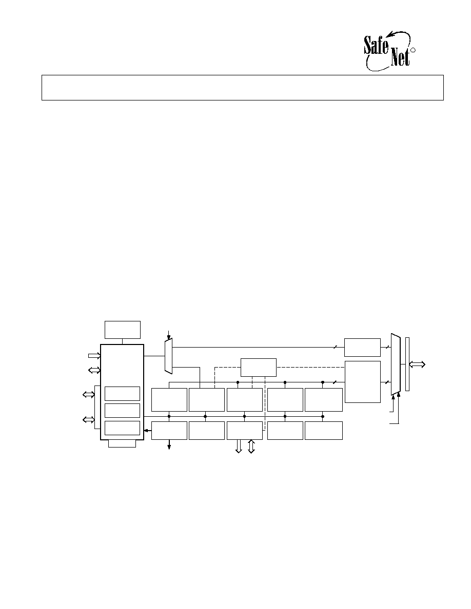
FUNCTIONAL BLOCK DIAGRAM
BUS_MODE
IDMA MODE
PCI MODE
IDMA
BUS
INTERRUPTS
FLAGS
SPORT 0
SERIAL
PORTS
SPORT 1
PROTECTED
KERNEL
RAM
(4K 16)
32
EXTERNAL
MEMORY
INTERFACE
RNG
BLOCK
PUBLIC KEY
ACCELERATOR
32-BITS
DATA
26-BITS
ADDR
LASER
VARIABLE
STORE
SERIAL
EEPROM
INTERFACE
INTERRUPT
CONTROLLER
APPLICATION
REGISTERS
RAM/ROM
PF7/
INT_H
DMA-32
CONTROLLER
IDMA
INTERFACE
16
PCI OR
CARDBUS
INTERFACE
32
16
BUS_MODE
BUS_SEL
16-
OR
32-BIT
BUS
KERNEL
MODE
CONTROL
KERNEL ROM
32K 24
PROG ROM
16K 24
DATA ROM
16K 16
TIMER
ADSP-218x
DSP CORE
EMI BUS
ENCRYPT
BLOCK
(DES, 3-DES)
HASH
BLOCK
(MD-5, SHA-1)
SafeNet is a registered trademark of Information Resource Engineering (IRE).
R

REV. 0
ADSP-2141L
2
PUBLIC KEY ACCELERATOR
Accelerator for Math-Intensive Public Key Operations
Diffie-Hellman Negotiate: <29 ms (1024-Bit Modulus,
180-Bit Exponent)
RSA 1024-Bit Sign: <29 ms; RSA 1024-Bit Verify: 6 ms
DSA Sign: <39 ms; DSA Verify: <66 ms
KEY MANAGEMENT BLOCK
Laser-Programmed Unique Triple-DES Cryptovariable
Protects Off-Chip Storage
Support for Secure Storage of Both Secret Keys and
Public/Private Key Pairs
Trust-Model Rules Enforcement
Only Encrypted Keys May Be Exported Off the Chip
Internal Key Cache for 15 Keys--Can Be Expanded to
700 Keys On-Chip
Keys May Also Be Securely Stored Off-Chip, Allowing
Unlimited Storage
DSP CORE
40 MIPS Sustained Performance
Single-Cycle Instruction Execution
Single-Cycle Context Switch
Zero-Overhead Looping
Low Power Dissipation
16K Words (16K 24) On-Chip Program RAM
16K Words (16K 16) On-Chip Data RAM
64M Words Off-Chip Program and Data Memory
Programmable 16-Bit Interval Timer with Prescale
PCI BUS/CARDBUS INTERFACE
32-Bit 3.3 V Bus Interface
33
MHz or 40
MHz* Bus Speed
Bus Master and Target Modes
Can Directly DMA Between Crypto Functions and Other
PCI Bus Agents
*66 MHz speed pending chip characterization.
GENERAL DESCRIPTION
The ADSP-2141L SafeNet DSP is a highly integrated embedded
security processor that incorporates a sophisticated, general
purpose DSP, along with a number of high performance Cryp-
tographic function blocks, as well as PCI, DMA and Serial
EEPROM interfaces. It is fabricated in 0.35
µ
CMOS triple-
layer metal technology and uses a 3.3 V power supply. It is
available in a 208-lead MQFP package with a commercial (0
°
C
to 70
°
C) temperature range.
DSP Core
The DSP is a standard Analog Devices ADSP-218x core with
full ADSP-2100 family compatibility. The ADSP-218x Core
combines the base DSP components from the ADSP-2100
family with the addition of two serial ports, a 16-bit internal
DMA port, a byte DMA port, a programmable timer, Flag I/O,
extensive interrupt capabilities, and on-chip program and data
memory. The external memory interface of the 218x core has
been extended to support up to 64M-words addressing for both
program and data memory. Some core enhancements have been
added in the ADSP-2141L, including on-chip security ROM
and interrupt functions. Refer to the Analog Devices ADSP-2183
data sheet for further information.
SafeNet CGX LibrarySecure Kernel
The SafeNet CGX Library is a crypto library embodied as firm-
ware (a secure kernel) that is mask-programmed into ROM within
the DSP. This solution protects the library from tampering. The
CGX Library provides the Application Programming Interface
(API) to applications that require security services from the
ADSP-2141L. Those applications may be software executing in
user mode on the DSP, or they may be external host software
accessing the ADSP-2141L via a PCI bus. Approximately 40
Crypto commands--called CGX (CryptoGraphic eXtensions)--
are provided at the API and a simple control block structure is
used to pass arguments into the secure kernel and return status.
The CGX library includes integrated drivers for the various
hardware crypto blocks on the chip. This allows the program-
mer to ignore those details and concentrate on other product
design issues.
The CGX library firmware runs under a protected mode state
of the DSP as described in the Kernel Mode Control section
following. This guarantees the security integrity of the system
during the execution of CGX processes and, for example, prevents
disclosure of cryptographic key data or tampering with a
security operation.
Kernel Mode Control
The Kernel Mode Control subsystem is responsible for enforcing
the security perimeter around the cryptographic functions of
the ADSP-2141L. The device may operate in either user mode
(kernel space is not accessible) or kernel mode (kernel space is
accessible) at a given time. When in kernel mode, the kernel RAM
and certain protected crypto registers and functions (kernel
space) are accessible only to the CGX library firmware. The
CGX Library executes host-requested macro-level functions
and then returns control to the calling application. The kernel
mode control subsystem resets the DSP should any security
violation occur, such as attempting to access a protected
memory location while in user mode.

REV. 0
ADSP-2141L
3
Protected Kernel RAM
The 4K
×
16 kernel RAM provides a secure storage area on the
ADSP-2141L for sensitive data such as keys or intermediate
calculations during public key operations. The Kernel Mode
Control subsystem (above) enforces the protection by allowing
only internal secure kernel mode access to this RAM. A public
keyset and a cache of up to 15 secret keys may be stored in kernel
RAM. Secure key storage may be expanded to 700 secret keys
by assigning segments of the DSP's internal data RAM to be
protected. Furthermore, a virtually unlimited number of data
encryption keys may be stored in an encrypted form in off-chip
memory.
Encrypt Block
The encrypt block performs high speed DES and Triple-DES
encrypt/decrypt operations. All four standard modes of DES are
supported: Electronic Code Book (ECB), Cipher Block Chaining
(CBC), 64-bit Output Feedback (OFB) and 1-bit, 8-bit and 64-
bit Cipher Feedback (CFB). The DES encrypt/decrypt operations
are highly pipelined and execute full 16-round DES in only four
clock cycles. Hardware support for padding insertion, verification
and removal further accelerates the encryption operation. Con-
text switching is provided to minimize the overhead of changing
crypto keys and Initialization Vectors (IVs) to nearly zero.
Hash Block
The secure hash block is tightly coupled with the encrypt block
and provides hardware accelerated one-way hash functions.
Both the MD-5 and SHA-1 algorithms are supported. Combined
operations that chain both hashing and encrypt/decrypt functions
are provided in order to significantly reduce the processing time
for data that needs both operations applied. For hash-then-encrypt
and hash-then-decrypt operations, the ADSP-2141L can perform
parallel execution of both functions from the same source and
destination buffers. For encrypt-then-hash and decrypt-then-hash
operations, the processing must be sequential, but minimum
latency is still provided through the pipeline chaining design. An
offset may be specified between the start of hashing and the
start of encryption to support certain protocols such as IPsec. A
`mutable bit handler' is also provided on the hash engine to
facilitate IPsec AH processing.
Random Number Generator (RNG) Block
The hardware random number generator provides a true, non-
deterministic noise source for the purpose of generating keys,
Initialization Vectors (IVs), and other random number require-
ments. Random numbers are provided as 16-bit words to the
kernel. The CGX kernel requests random numbers as needed to
perform requested CGX commands such as CGX_Gen_Key,
and can also directly supply from 1 to 65,535 random bytes to a
host application via the CGX_Random command.
Public Key Accelerator
The public key accelerator module works in concert with the
CGX kernel firmware to provide full public key services to the
host application. The kernel provides macro-level functions to
perform Diffie-Hellman key agreement, RSA encrypt or decrypt,
DSA compute and verify digital signatures. The hardware accel-
erator block speeds computation-intensive operations such as
large vector multiply, add, subtract, square.
PCI/Cardbus Interface
A full 40 MHz/33 MHz PCI bus interface has been added to the
core DSP functions. The 32-bit PCI interface supports both bus
master and target modes. The ADSP-2141L is capable of using
DMA to directly access data on other PCI entities and pass that
data through its encryption/hash engines.
32-Bit DMA Controller
The ADSP-2141L incorporates a high performance 32-bit DMA
controller which can be set up to move data efficiently between
Host PCI memory, the hash/encrypt blocks, and/or external
memory. The DMA controller can be used with the PCI bus in
master mode, thus autonomously moving 32-bit data with mini-
mal DSP intervention. Up to 255 long words (1020 bytes) can
be moved in a burst at up to 160 Mbytes per second.
Application Registers
The application registers are a set of memory-mapped registers
that facilitate communications between the ADSP-2141L and a
host processor via the PCI bus. One of the registers is a mailbox
that is 44 bytes long and set up to hold the CGX command
structure passed between the host and DSP processors. The
application registers also provide the mechanism that allows the
DSP and the external host to negotiate ownership of the hash/
encrypt block.
Serial EEPROM Interface
The serial EEPROM interface allows an external nonvolatile
memory to be connected to the ADSP-2141L for storing PCI
configuration information (Plug and Play), as well as general-
purpose nonvolatile storage. For example, encrypted (black)
keys could be stored into EEPROM for fast recovery after a
power outage.
Interrupt Controller
The DSP core provides support for 14 interrupt sources, includ-
ing six external and eight internal. All interrupts are prioritized
into 12 levels and interrupt nesting may be enabled or disabled
under software control. The security block interrupt controller
provides enhancements to the DSP interrupt functions.
Primarily, the interrupt controller provides a new interrupt
generation capability to the DSP or to an external host processor.
Under programmable configuration control, a crypto interrupt
may be generated due to completion of certain operations such
as encrypt complete, hash complete. The interrupt may either
be directed at the DSP core (on
IRQ2), or provided on an out-
put line (PF7/
INT_H) to a host subsystem.
Laser Variable Storage
The laser variable storage consists of 256 bits of tamper-proof
factory-programmed data that is only accessible to the internal
function blocks and the security kernel. Included in these laser
variable bits are:
·
Local Storage Variable (master key-encryption key)
·
Randomizer Seed (to supplement the true entropy fed into
the RNG)
·
Program Control Data (enables/disables various features and
configures the ADSP-2141L)
·
CRC of the Laser Data (to verify laser data integrity).
REV. 0
ADSP-2141L
4
The Program Control Data Bits (PCDBs) include configuration
for permitted key lengths, algorithm enables, Red KEK loading.
Most of the PCDB settings may be overridden with a digitally
signed token which may be loaded into the ADSP-2141L when
it boots. These tokens are created by IRE and each is targeted to
a specific ADSP-2141L using a hash of its unique identity.
Downloadable Secure Code
The ADSP-2141L allows additional security functions to be added
to the device through a secure download feature. Up to 16K
words of code may be downloaded into internal memory within
the DSP and this code can be given the security privileges of the
CGX kernel firmware. All downloaded firmware is authenticated
with a digital signature and verified with an on-chip public key.
Additional functions could include new encryption, hash or
public key algorithms such as IDEA, RC-4,
RIPEMD, elliptic
curve, or any other application that needs direct control over the
protected cryptographic hardware.
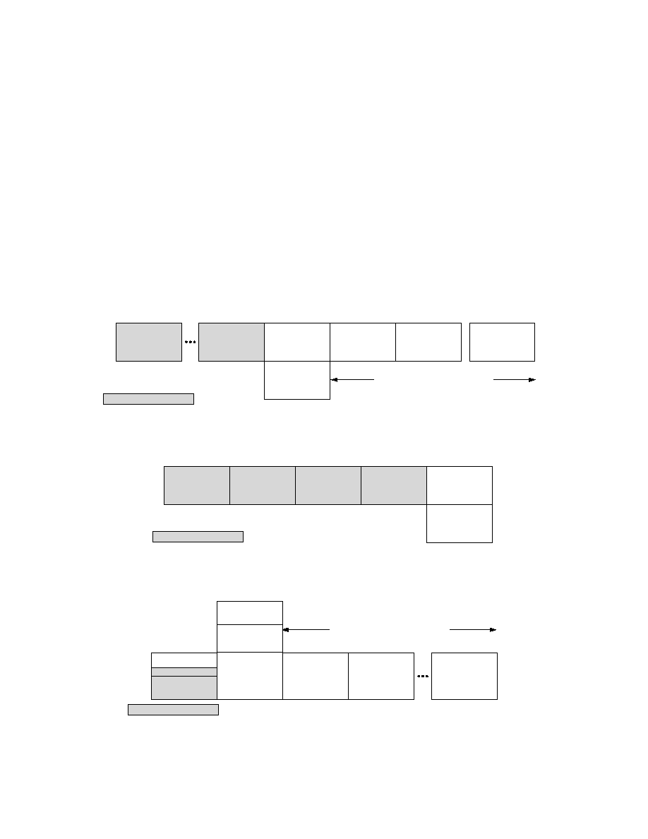
8K KERNEL TOP
KERNEL MODE
(PMOVLAYL = C)
(PMOVLAYH = 000)
8K KERNEL BASE
KERNEL MODE
(PMOVLAYL = F)
(PMOVLAYH = 000)
8K INTERNAL
PAGE
(PMOVLAYL = 0)
(PMOVLAYH = 000)
8K EXTERNAL
PAGE = 0
(PMOVLAYL = 1)
(PMOVLAYH = 000)
8K EXTERNAL
PAGE 1
(PMOVLAYL = 2)
(PMOVLAYH = 000)
8K KERNEL
PAGE 8191
(PMOVLAYL = 2)
(PMOVLAYH = FFF)
0x3FFF
0x2000
8K INTERNAL
(COMMON BANK)
0x1FFF
0x0000
UP TO 64 MEGAWORDS
EXTERNAL PROGRAM MEMORY
(PMOVLAYL ALTERNATES 2, 1, 2, 1...)
PMOVLAYL = LS NIBBLE OF PMOVLAY
PMOVLAYH = MS 3 NIBBLES OF PMOVLAY
SHADED = KERNEL SPACE
Figure 1. Program Memory (MMAP = 0)
8K KERNEL TOP
KERNEL MODE
(PMOVLAYL = C)
(PMOVLAYH = 000)
8K INTERNAL
(PMOVLAYL = 0)
(PMOVLAYH = 000)
0x3FFF
0x2000
0x1FFF
0x0000
PMOVLAYL = LS NIBBLE OF PMOVLAY
PMOVLAYH = MS 3 NIBBLES OF PMOVLAY
SHADED = KERNEL SPACE
8K KERNEL
KERNEL MODE
(PMOVLAYL = D)
(PMOVLAYH = 000)
8K KERNEL
KERNEL MODE
(PMOVLAYL = E)
(PMOVLAYH = 000)
8K KERNEL
KERNEL MODE
(PMOVLAYL = F)
(PMOVLAYH = 000)
8K EXTERNAL
Figure 2. Program Memory (MMAP = 1)
MEMORY-MAPPED
REGISTERS
PROTECTED
4K KERNEL RAM
(DMOVLAY = 000F)
KERNEL MODE
8K INTERNAL
(DMOVLAYL = 0)
(DMOVLAYH = 000)
8K EXTERNAL
PAGE = 0
(DMOVLAYL = 1)
(DMOVLAYH = 000)
8K EXTERNAL
PAGE 1
(DMOVLAYL = 2)
(DMOVLAYH = 000)
0x2000
UP TO 64 MEGAWORDS
EXTERNAL DATA MEMORY
(DMOVLAYL ALTERNATES 2, 1, 2, 1...)
SHADED = KERNEL SPACE
8K KERNEL
PAGE 8191
(DMOVLAYL = 2)
(DMOVLAYH = FFF)
32
MEMORY-MAPPED
REGISTERS
8160 WORDS
INTERNAL
0x1FFF
0x1800
0x17FF
0x1000
0x0FFF
0x0000
0x3FFF
0x3FE0
0x3FDF
Figure 3. Data Memory
ARCHITECTURE OVERVIEW
This section provides an architecture-level description of the
unique function blocks within the ADSP-2141L.
Memory Map
The ADSP-2141L memory map is very similar to that of the
ADSP-2183 DSP, except that it includes significantly more off-
chip memory addressing, and has additional crypto registers
which are accessible to the user.
DSP Core
The DSP core is architecturally identical to the ADSP-218x
with a few exceptions.
·
The memory map includes additional external memory
addressing through the PMOVLAY and DMOVLAY mecha-
nisms. For more information, see the Memory Map section.
·
Additional memory-mapped crypto registers are available in
the kernel data RAM space.
·
The PF7/
INT_H flag pin may be reassigned to be the host
interrupt output.
REV. 0
ADSP-2141L
5
·
IRQ2 now can include interrupt sources from the crypto
subsystem, depending on interrupt mask registers.
·
A new read register has been added to indicate the state of
interrupt enable and interrupt masks.
·
The kernel mode control subsystem has been added to super-
vise the protected mode of operation of the DSP core.
·
Internal RAM protection logic has been added to allow the
kernel to seize increments of 1K word of internal PRAM and
DRAM.
·
Bus mode configuration (218x vs. PCI) pins have been added.
·
32K words of kernel program ROM have been added to the
DSP memory space. (See the Memory Map section.)
Kernel Mode Control
The kernel mode control subsystem provides the following
functions which serve to enforce the security integrity of the
ADSP-2141L:
·
Provide a means to securely enter the kernel mode.
·
Provide a means to properly exit the kernel mode.
·
Prevent user mode access to protected memory and register
locations.
·
Manage interrupts during kernel mode executions.
·
Manage the reset function to ensure that sensitive variables
in DSP registers are erased.
Most of the kernel mode control functions are implemented in
the hardware of the ADSP-2141L and are not directly visible to
nonkernel applications (user mode). Any attempt by a user
mode application program running on the DSP to access a
kernel space addresses (PRAM 0x2001 0x3FFF, PMOVLAY
000C 000F; or DRAM 0x0000 0x17FF, DMOVLAY 000F)
results in an immediate chip reset and all sensitive registers and
memory locations are erased. Kernel mode may only be entered
via a call, jump or increment to address 0x2000 with PMOVLAY
set to 0x000F. Once in kernel mode, any branch to nonkernel
space program memory causes the DSP to return to user mode.
(Note: For security reasons when in kernel mode, the DSP does
not respond to Emulator bus requests.)
The kernel mode can be interrupted during execution; however,
during certain periods where sensitive data is being moved, all
interrupts are disabled. Within the interrupt service routine,
another call to the kernel (CGX call) may be made if desired,
although there are limitations on which CGX commands may
preempt another. (For information, see the ADSP-2141L CGX
Interface Programmer's Guide http://www.ire-ma.com/proddoc.htm.)
Only one level of kernel mode nesting is permitted. An interrupt
to a user mode vector location while in nested kernel mode will
also trigger the violation reset logic.
Once the interrupt service routine is finished, the return-from-
interrupt must return control back to the kernel at the address/
overlay that was originally interrupted, otherwise the protection
logic will issue a chip reset.
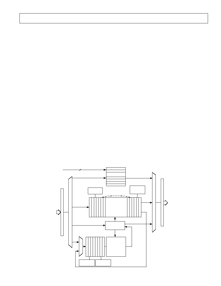
Hash and Encrypt Block Overview
The encrypt block is tightly coupled to the hash block in the
ADSP-2141L and therefore the two are discussed together.
Refer to Figure 4, Hash/Encrypt Functional Block Diagram, for
the following description.
The algorithms implemented in the combined hash and encryp-
tion block are: DES, Triple DES, MD-5 and SHA-1. Data can
be transferred to and from the module once to perform both
hashing and encryption on the same data stream. The DES
encrypt/decrypt operations are highly paralleled and pipelined,
and execute full 16-round DES in only four clock cycles. The
internal data flow and buffering allows parallel execution of
hashing and encryption where possible, and allows processing of
data concurrently with I/O of previous and subsequent blocks.
PAD
CONSUME
AND VERIFY
WRITE
CONTEXT
HASH
DIGEST
READ
CONTEXT
RD
DSP
OR
PCI
16-/32-BIT
OUTPUT
BUS
WR
REGISTER
ADDRESS
DSP
OR
PCI
16-/32-BIT
INPUT
BUS
ENCRYPT/
DECRYPT
BLOCK
CONTEXT
STORAGE (0/1)
HASH
BLOCK
PAD
INSERTION
512-BIT
FIFO
(ENCRYPT-THEN-HASH)
(DECRYPT-THEN-HASH)
7
512-BIT
FIFO
MUTABLE BIT
PROCESSING
PAD
INSERTION
Figure 4. Hash/Encrypt Functional Block Diagram

REV. 0
ADSP-2141L
6
Context switching is optimized to minimize the overhead of
changing cryptographic keys to near zero.
The software interface to the module consists of a set of
memory-mapped registers, all of which are visible to the DSP and
most of which can be enabled for host access via the PCI bus. A
set of five, 16-bit registers define the operation to be performed,
the length of the data buffer to be processed, in bytes, the offset
between the start of hashing and encryption (or vice versa), and
the padding operation. If the data length is unknown at the time
the encrypt/decrypt operation is started, the data length register
may be set to zero, which specifies special handling. In this case,
data may be passed to the hash/encrypt block indefinitely until
the end of data is encountered. At that time, the operation is
terminated by writing a new control word to the hash/encrypt
control register (either to process the next packet or to invoke
the idle state if there is no further work to do). This will close
out the processing for the packet, including the addition of the
selected crypto padding.
A set of seven status registers provides information on when a
new operation can be started, when there is space available to
accept new data, when there is data available to be read out, and
the results from the padding operation.
Crypto Contexts
There are two sets of crypto-context registers. Each context
contains a DES or triple DES key, initialization vector, and
precomputed hashes (inner and outer) of the authentication key
for HMAC operations. The contexts also contain registers to
reload the byte count from a previous operation (which is part
of the hashing context), as well as an IV (also called salt) for
decrypting a black key, if necessary.
Once a crypto-context has been loaded and the operation
defined, data is processed by writing it to a data input FIFO. At
the I/O interface, data is always written to, or read from, the
same address. Internally, the hash and encryption functions
have separate 512-bit FIFOs, each with their own FIFO man-
agement pointers. Incoming data is automatically routed to one
or both of these FIFOs, depending on the operation in progress.
Output from the encryption block is read from the data output
FIFO. In encrypt-hash or decrypt-hash operations, the data is
also automatically passed to the hashing data input FIFO. Output
from the hash function is always read from the digest register of
the appropriate crypto-context.
The initialization vector to be used for a crypto operation can be
loaded as part of a crypto-context. When an operation is complete,
the same context will contain the resulting IV produced at the
end, which can be saved away and restored later to continue the
operation with more data.
In certain packet-based applications such as IPsec, a feature is
available that avoids the need for the control software to generate
and load random IVs for outgoing (encrypted) packets. Effec-
tively, the IV register can be configured to be automatically
updated with new random numbers for each encrypted packet,
with almost no software intervention.
Padding
When the input data is not a multiple of eight bytes (a 64-bit
DES block), the encrypt module can be configured to automati-
cally append pad bytes. There are several options for how the
padding is constructed, which are specified using the pad control
word of the operation description. Options include zero padding,
pad-length character padding (PKCS#7), incrementing count,
with trailing pad length and next header byte (for IPsec), or
fixed character padding. Note that for the IPsec and PKCS#7
pad protocols, there are cases where the padding not only fills
out the last 8-byte block, but also causes an additional 8-byte
block of padding to be added.
For the hash operations, padding is automatically added as
specified in the MD-5 and SHA-1 standards. When the hash
final command is issued indicating the last of the input data, the
algorithm-specified padding and data count bits are added to the
end of the hash input buffer prior to computing the hash.
Data Offsets
Certain security protocols, including IPsec, require portions of a
data packet to be hashed while the remainder of the data is both
hashed and encrypted. The ADSP-2141L supports this require-
ment through the OFFSET register, which allows specifying the
number of 32-bit dwords of offset between the hash and encrypt/
decrypt operations.
Black Key Loads
The cryptographic keys loaded as part of a crypto-context can
be stored off-chip in a black, or encrypted, form. If the appropri-
ate control bit is set (HECNTL Bit 15), the DES or 3-DES key
will be decrypted immediately after it is written into the context
register. The hardware handles this decryption automatically.
The Key Encryption Key (KEK) that covers the black keys
is loaded in a dedicated write-only KEK register within the
ADSP-2141L. The IV for decrypting the black secret key is
called `salt' and must be stored along with the black key (as part
of the context). Note that 3-DES CBC mode is used for pro-
tecting 3-DES black keys and single DES CBC is used for
single DES black keys.
When black keys are used, the key-decrypt operation adds a
6-cycle overhead (0.15
µ
s @ 40 MHz) for DES keys or 36-cycle
overhead (0.9
µ
s @ 40 MHz) for triple DES keys each time a
new crypto-context is loaded. (Note that if the same context is
used for more than one packet operation, the key decryption does
not need to be performed again.) Depending on the sequencing
of operations, this key decryption may in fact be hidden (from a
performance impact perspective) if other operations are underway.
This is because the black key decryption process only requires
that the DES hardware be available. For example, if the DSP is
reading the previous hash result from the output FIFO, the
black key decryption can be going on in parallel. Also note that
the data driver firmware does NOT have to wait for the key to
be decrypted before writing data to the input FIFO. The hard-
ware automatically waits for the key to be decrypted before
beginning to process data for a given packet. So, with efficient
pipeline programming, it is possible to make the impact of black
key essentially zero.
The KEK for key decryption is loaded via the secure kernel
firmware using one of the CGX key manipulation commands.
(For more information, see the Command Summary section.)
This KEK is typically the same for all black keys, since it is usually
protecting local storage only. It is designated the DKEK in the
CGX API.
One of the laser-programmed configuration bits specifies whether
red (plaintext) keys are allowed to be loaded into the ADSP-
2141L from a host. If the AllowRedKeyLoad laser bit is not set,
keys may only be loaded in their black form. This is useful in
systems where export restrictions limit the key length that may
be used or where the external storage environment is untrusted.
REV. 0
ADSP-2141L
7
If the AllowRedKeyLoad bit is set, keys may be loaded either in
their black form, or in the red or unencrypted form. Note that
the laser configuration bit may be overridden with a signed
enabler token. (For more information, see the Laser Variable
Storage section.)
Depending on the definition of the security module boundary in
a given application, FIPS 140-1 may require the use of black
keys to protect key material. In other words, if the security
boundary does not enclose the database where keys are stored,
those keys must be protected from compromise. Black key is a
satisfactory way to meet this FIPS requirement.
Random Number Generator (RNG) Block
The random number generator is designed to provide highly
random, nondeterministic binary numbers at a high delivery rate
with little software intervention. The random numbers are acces-
sible to the kernel firmware in a 16-bit register that may be read
by the DSP in kernel mode. Once the register is read, the RNG
immediately generates a new 16-bit value that is available within
12 microseconds.
All application-level access to random numbers should occur
through the Kernels CGX_RANDOM command (see the
Command Summary section).
The random number generator is designed using a "shot noise"
true entropy source which is sampled by the master 40 MHz
clock of the ADSP-2141L. The entropy source then feeds a
complex nonlinear combinatorial circuit that produces the final
RNG output based on the interaction of the entropy source and
the 40 MHz system clock. Over 200 stages of Linear Feedback
Shift Register (LFSR) are incorporated into the RNG design.
In order to facilitate FIPS 140-1 compliance, an option may be
selected during CGX kernel initialization to enable an ANSI
X9.17 Annex C post-randomizer to be applied to the output of
the RNG. This randomizer applies the DES ECB algorithm
multiple times to further disperse and whiten the random source.
Although this is not necessary to ensure the quality of the random
numbers, it meets the criteria for a NIST-approved random num-
ber generation algorithm.
Public Key Accelerator (PKAC)
The public key arithmetic coprocessor (otherwise known as a
BigNum processor) is designed to support long vector calcula-
tions of the kind needed to perform RSA, Diffie-Hellman and
Elliptic Curve operations.
The PKAC can perform multiplication, squaring, addition and
subtraction on arbitrary length bit vectors. The CGX software is
responsible for setting the address register for the operands and
result, as well as specifying the length and operation type. Once
the operation type field is written, the processor polls the opera-
tion complete status while the calculation is carried out.
The PKAC utilizes the protected kernel RAM for input, output
and intermediate variable storage. It may only be accessed from
the secure kernel mode. Since public key computations typically
take many milliseconds to complete, they may be preempted
using a DSP interrupt.
Most application interaction with the public key accelerator will
occur via the CGX software interface (see the Command Inter-
face section). Both high level public key operations such as RSA
Sign or Create Diffie-Hellman Key, as well as primitive operations
such as Multiply Vector, Add Long Vector, etc., are presented
via the CGX interface.
PCI/Cardbus Interface
The ADSP-2141L appears as a target on the PCI Bus as a single
contiguous memory space of 128k bytes. In this memory space,
the host can access the following:
·
The unprotected internal crypto registers of the ADSP-2141L
·
IDMA access to the DSP's internal program memory (PM)
and data memory (DM)
·
Paged access to external memory connected to the
ADSP-2141L
·
The Kernel RAM (KRAM) if it has been unprotected by an
extended mode program
As a PCI Master, the ADSP-2141L can transfer data between:
·
The unprotected internal crypto registers and FIFOs of the
ADSP-2141L and PCI Host memory
·
External memory and PCI Host memory
A 32-bit DMA engine within the ADSP-2141L facilitates these
transfers and permits full PCI bandwidth use.
Serial EEPROM Interface
The serial EEPROM interface allows the ADSP-2141L to auto-
matically read the PCI configuration parameters at chip power-up.
IRE can provide the data content for the EEPROM to properly
set the chip device vendor ID, type and properties for full com-
pliance with the PCI Plug and Play standards.
In addition to being used for storage of host bus parameters, any
extra space in the EEPROM may be accessed by the DSP, either
in user mode or kernel mode. Support for this function is not
included in the standard CGX command set. Refer to the
ADSP-2141 User's Manual for the information on the data
contents of the EEPROM. Refer to http://www.analog.com/
industry/dsp/ire.html.
Table I. Interrupt Sources
Internal Interrupt Sources
External Interrupt Sources
Interrupt
Notes
Interrupt
Notes
Reset
or Power-Up (PUCR = 1)
IRQ2
Edge- or Level-Sensitive
Power-Down
IRQL1
Level-Sensitive
SPORT0 Transmit
IRQL0
Level-Sensitive
SPORT0 Receive
IRQE
Edge-Sensitive
BDMA Interrupt
IRQ1
Edge- or Level-Sensitive
SPORT1 Transmit
Mixed with IRQ1
IRQ0
Edge- or Level-Sensitive
SPORT1 Receive
Mixed with IRQ0
Timer
REV. 0
ADSP-2141L
8
Interrupt Controller
The DSP core of the ADSP-2141L provides a powerful set of
interrupt sources. A total of 14 interrupt sources are available,
although two pairs are multiplexed, yielding 12 simultaneous
sources. Refer to Table I.
The ADSP-2141L enhances the existing interrupt controller
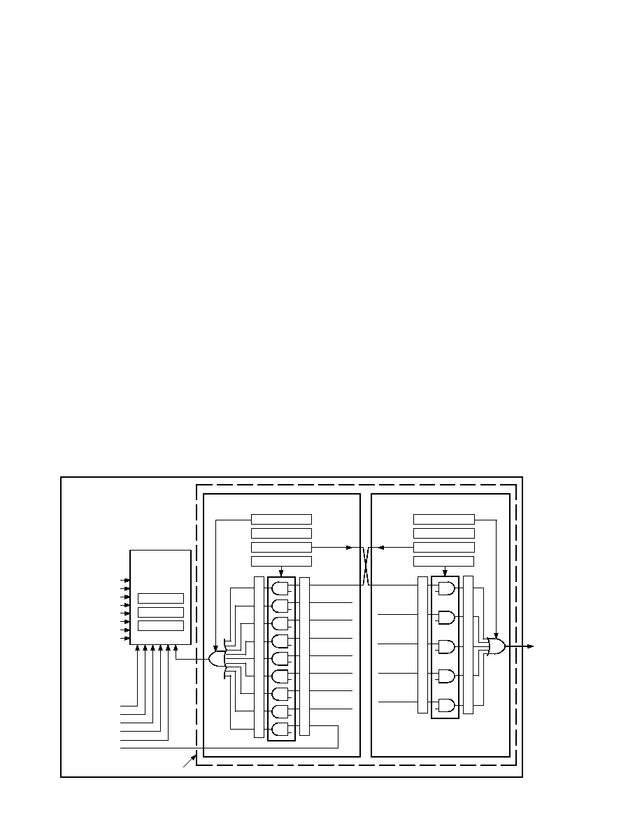
within the ADSP-218x DSP Core with some additional func-
tions related to the crypto functional blocks and the external
host bus interfaces. Two additional interrupt controller sub-
systems have been added to the basic interrupt controller as
shown in Figure 5.
The DSP interrupt controller allows programming between one
and nine sources for the IRQ2 interrupt to the DSP. The
DIMASK register provides the mask to select which interrupt
source is enabled. A pair of status registers, DUMSTAT and
DMSTAT, allow the DSP firmware to read the status of any
interrupt source either before or after the mask is applied.
The host interrupt controller allows programming between one
and five sources for the PF7/
INT_H interrupt output signal
(which may be connected to the interrupt input of the host
system). The HMASK register provides the mask to select which
interrupt source is enabled. A pair of status registers, HUMSTAT
and HMSTAT, allow the host firmware to read the status of any
interrupt source either before or after the mask is applied.
Laser Variable Storage
The laser variables are configured through 256 Fuses in the
ADSP-2141L, which are programmed during IC manufacture.
Each ADSP-2141L produced is programmed with a unique set
of Laser Variables.
·
Local Storage Variable (LSV--the Master Key-Encryption-Key)
·
Internal Seed Variable
H/E CONTEXT0
DONE
DICLR
DIFRC
DIMASK
HOST
INTERRUPT
H/E CONTEXT1
DONE
HOST
WROTE CMD
DMA xFER
DONE
DMA xFER
QUEUED
EXT MEM
CONFLICT
IRQ2
DICFG
DSP INTERRUPT CONTROLLER
DSP
INTERRUPT
INTH
TO HOST
CRYPTO INTERRUPT
SUBSYSTEM BOUNDRY
HOST UNMASKED STATUS REGISTER
DSP
WROTE
CMD
HASH/ENC
ERROR
HASH/ENC
ERROR
HICLR
HIFRC
HIMASK
HICFG
HOST INTERRUPT CONTROLLER
IFC
IRQ2
ADSP-2183
INTERRUPT
CONTROLLER
IMASK
ICNTL
RESET
POWER DOWN
SPORT0 Tx
SPORT0 Rx
BDMA INT
TIMER INT
SPORT1 Tx
SPORT1 Rx
INTERNAL
INTERRUPTS
IRQE
IRQL0
IRQL1
IRQ0
IRQ1
IRQ2
EXTERNAL
INTERRUPTS
DSP
DSP MASKED STATUS REGISTER
DSP UNMASKED STATUS REGISTER
HOST MASKED STATUS REGISTER
H/E CONTEXT1
DONE
H/E CONTEXT0
DONE
Figure 5. Interrupt Controller Block Diagram
·
48-Bit Program Control Data (enables/disables various fea-
tures and configures the ADSP-2141L)
·
CRC of the Laser Data (to verify integrity of the laser bits)
The LSV is a unique triple DES master key-encrypting key that
allows the ADSP-2141L to securely store data (primarily other keys)
off-chip for later reloading. This is necessary if more storage space
is needed than is available with on-chip RAM, or if keys need to
be saved and restored after a power outage. Each ADSP-2141L
produced is programmed with a unique, randomly generated
local storage variable.
The internal seed variable is used to randomly initialize the
RNG circuits before the entropy is mixed in. Each ADSP-2141L
produced is programmed with a unique, randomly generated
internal seed variable which is loaded into the RNG at chip boot
time and cannot ever be read by software.
The 48 Program Control Data Bits (PCDBs) include configura-
tion for permitted key lengths, algorithm enables, red KEK
loading, internal IC pulse timing characteristics. The PCDBs
provide configuration data that falls into three categories:
· Internal IC pulse-timing characteristics
· ADSP-2141L hardware version number field
· ADSP-2141L feature enables
The first two categories consist of data that cannot be altered
once the ADSP-2141L has been fabricated.
The feature enables can be overridden using a factory token
enabler which may be passed to the CGX kernel as part of the
CGX_INIT command. This token is digitally signed with an
IRE private key and verified internal to the ADSP-2141L with
its public key. The CGX_INIT command is documented in the
ADSP-2141 CGX Interface Programmer's Guide (available from
http://www.ire-ma.com/proddoc.htm).

REV. 0
ADSP-2141L
9
PIN FUNCTIONS
I/O Descriptions
This section describes the physical I/O hardware on the ADSP-2141L.
PIN FUNCTION DESCRIPTIONSI/O Hardware
# of
Input/
Pin Name
Pins
Output
Function
External Memory Bus
Address [25:0]
26
O
Address Output Pins for Program, Data, Byte and I/O Spaces (13 Bits 2183, 13 Bits
from Overlay Register) Note: A0 not used for 32-bit memory.
Data [31:0]
32
I/O
Data I/O Pins for Program and Data Memory Spaces
D31:0 are used for wide-bus data memory.
D23:0 are used for DSP Program RAM.
D23:8 are used for I/O Space.
D23:8 are used for DSP Data RAM.
D15:8 are used for byte memory.
D23:16 are also used as Byte Space Addresses
Interrupts
IRQ2
1
I
Edge- or Level-Sensitive Interrupt Request
IRQL0
1
I
Level-Sensitive Interrupt Requests
IRQL1
1
I
Level-Sensitive Interrupt Requests
IRQE
1
I
Edge-Sensitive Interrupt Request
Bus Signals
BR
1
I
Bus Request Input
BG
1
O
Bus Grant Output
BGH
1
O
Bus Grant Hung Output
PMS
1
O
Program Memory Select Output
DMSL
1
O
Data Memory Select Output (Lower 16 Bits for 32-Bit DM)
DMSH
1
O
Upper Memory Select Output (Upper 16 Bits for 32-Bit DM, Not Used for 16-Bit DM)
BMS
1
O
Byte Memory Select Output
IOMS
1
O
I/O Space Memory Select Output
CMS
1
O
Combined Memory Select Output (
PMS, DMS*, IOMS, BMS)
RD
1
O
Memory Read Enable Output
WR
1
O
Memory Write Enable Output
Miscellaneous
MMAP
1
I
Memory Map Select Input (1 = Overlay External at 0x0000)
BMODE
1
I
Boot Option Control Input (0 = BDMA, 1 = IDMA)
CLKIN, XTAL
2
I
Clock or Quartz Crystal Input (1/2 of the ADSP-2141 Clock)
CLKOUT
1
O
Processor Clock Output
Serial Ports
SPORT0
SCLK0
1
I/O
Serial Port 0 Clock
DR0
1
I
Serial Port 0 Receive Data Input
RFS0
1
I/O
Serial Port 0 Receive Frame Sync
DT0
1
O
Serial Port 0 Transmit Data Output
TFS0
1
I/O
Serial Port 0 Transmit Frame Sync
SPORT1
Port Configuration
(System Control Reg) >
1 = Serial Port
0 = Other
SCLK1
1
I/O
Serial Port 1
Clock
DR1
1
I
Serial Port 1 Receive Data Input
Flag In
RFS1
1
I/O
Serial Port 1 Receive Frame Sync
IRQ0
DT1
1
O
Serial Port 1 Transmit Data Output
Flag Out
TFS1
1
I/O
Serial Port 1 Transmit Frame Sync
IRQ1
Power-Down
PWD
1
I
Power-Down Initiate Control
PWDACK
1
O
Power-Down Acknowledge

REV. 0
ADSP-2141L
10
# of
Input/
Pin Name
Pins
Output
Function
Flags
PF6:0
7
I/O
Programmable I/O Pins
PF7/
INT_H
1
I/O
Programmable I/O PinorInterrupt Output (Host Mode)
Emulator
EE
1
(Emulator Only)
EBR
1
(Emulator Only)
EBG
1
(Emulator Only)
ERESET
1
(Emulator Only)
EMS
1
(Emulator Only)
EINT
1
(Emulator Only)
ECLK
1
(Emulator Only)
ELIN
1
(Emulator Only)
ELOUT
1
(Emulator Only)
Serial EEPROM Interface
EE_DI
1
O
Serial EEPROM Data In
EE_DO
1
I
Serial EEPROM Data Out
EE_CS
1
O
Serial EEPROM Chip Select
EE_SK
1
O
Serial EEPROM Clock
Bus Select
BUS_MODE
1
I
Processor Bus Select
BUS_SEL
1
I
Bus Select
PCI Bus (Dedicated Pins)
PCI_CLK
1
I
PCI Clock
PCI_PAR
1
I/O
PCI Parity Bit
PCI_IRDY
1
I/O
PCI Initiator Ready
PCI_STOP
1
I/O
PCI Abort Transfer
*When
DMS is enabled for generation of CMS, the CMS is activated for DSP access to external memory only, NOT for DMA controller accesses.
Bus Mode Descriptions
The Pin Function Descriptions, Bus Mode table, shows the multiplexed pins in 2183 and PCI mode. For more information on the
PCI pins MPLX1MPLX12, see the Pin Functions DescriptionPCI Mode Multiplex Bus table on the following page.
PIN FUNCTION DESCRIPTIONS--Bus Mode
# of
Input/
2183 Mode
PCI Mode
Bus Mode
Pins
Output
(bus_mode = 0, bus_sel = 0)
(bus_mode = 1, bus_sel = 0)
MPLX_RESET
1
I
RESET_1
Pci_
rst
MPLX1
1
I/O
Pci_
cbe3
MPLX2
1
I/O
Pci_
cbe2
MPLX3
1
I/O
Pci_
cbe1
MPLX4
1
I/O
Pci_
cbe0
MPLX5
1
I
IRD
Pci_idsel
MPLX6
1
I
IWR
Pci_
gnt
MPLX7
1
I/O
IS
Pci_
frame
MPLX8
1
I/O
IAL
Pci_
devsel
MPLX9
1
I/O
IACK
Pci_
trdy
MPLX10
1
I/O
FL0
Pci_
perr
MPLX11
1
I/O
FL1
Pci_
serr
MPLX12
1
O
FL2
Pci_
req
MPLX_BUS[31:0]
32
I/O
IAD15:0
Pci_ad15:0
N/C 31:16
Pci_ad31:16
Power
GND
24
Ground Pins
VDD
22
Power Supply Pins (3.3 V)
Total:
208
Includes the pins from this table and the I/O Hardware Pin Function Description table.
REV. 0
ADSP-2141L
11
IDMA Mode Multiplex Bus Pin Definition
IDMA Port (218x Mode)
PIN FUNCTION DESCRIPTIONS--IDMA Mode Multiplex Bus
Pin Name
IDMA Name
Pins
I/O
Description
MPLX5
IRD
1
I
IDMA Port Read Input
MPLX6
IWR
1
I
IDMA Port Write Input
MPLX7
IS
1
I
IDMA Port Select
MPLX8
IAL
1
I
IDMA Port Address Latch
MPLX9
IACK
1
O
IDMA Port Access Ready Acknowledge
MPLX10
FL0
1
O
Output Flags
MPLX11
FL1
1
O
Output Flags
MPLX12
FL2
1
O
Output Flags
MPLX_BUS
IAD
16
I/O
IDMA Data I/O
PCI Port
PIN FUNCTION DESCRIPTIONS--PCI Mode Multiplex Bus
Pin Name
PCI Name
Pins
I/O
Description
MPLX1
Pci_
cbe3
1
I/O
Bus Command / Byte Enable 3
MPLX2
Pci_
cbe2
1
I/O
Bus Command / Byte Enable 2
MPLX3
Pci_
cbe1
1
I/O
Bus Command / Byte Enable 1
MPLX4
Pci_
cbe0
1
I/O
Bus Command / Byte Enable 0
MPLX5
Pci_idsel
1
I
Initialization Device Select
MPLX6
Pci_
gnt
1
I
Bus Grant
MPLX7
Pci_
frame
1
I/O
Cycle Frame
MPLX8
Pci_
devsel
1
I/O
Device Select
MPLX9
Pci_
trdy
1
I/O
Target Ready
MPLX10
Pci_
perr
1
I/O
Parity Error
MPLX11
Pci_
serr
1
I/O
System Error
MPLX12
Pci_
req
1
O
PCI Bus Request
MPLX_BUS
Pci_ad15:0
Pci_ad31:16
32
I/O
PCI Address/Data Bus
PF7/
INT_H
Pci_
intA
1
O
PCI Interrupt A Request
SYSTEM INTERFACE
The ADSP-2141L may be integrated into a wide variety of sys-
tems, including those that already have a microprocessor and
those that will use the ADSP-2141L as the main processor. The
device can be configured into one of two Host Bus modes:
IDMA or PCI.
IDMA Bus Mode
The IDMA bus mode operates the same as in a native ADSP-
218x device, as described in this section.
The IDMA port provides an efficient means of communication
between a host system and the ADSP-2141L. The port is used
to access the on-chip program memory and data memory of the
DSP with only one DSP cycle per word overhead. The IDMA
port cannot, however, be used to write to the DSP's memory-
mapped control registers.
The IDMA port has a 16-bit multiplexed address and data bus,
and supports reading or writing 16-bit data (DM) or 24-bit
program memory (PM). The IDMA port is completely asyn-
chronous and can be written to while the ADSP-2141L is oper-
ating at full speed.
The DSP memory address is latched and then automatically
incremented after each IDMA transaction. An external device can
therefore access a block of sequentially addressed memory by
specifying only the starting address of the block. This increases
throughput as the address does not have to be sent for each
memory access.
The IDMA port access occurs in two phases. The first is the
IDMA address latch cycle. When the acknowledge is asserted, a
14-bit address and 1-bit destination type can be driven onto the
bus by an external device. The address specifies an on-chip
memory location; the destination type specifies whether it is a
DM or PM access. The falling edge of the address latch signal
latches this value to the IDMAA register.
Once the address is stored, data can either be read from or
written to the ADSP-2141L's on-chip memory. Asserting the
select line (
IS) and the appropriate read or write line (IRD and
IWR respectively) signals the ADSP-2141L that a particular
transaction is required. In either case, there is a one-processor-
cycle delay for synchronization. The memory access consumes
an additional processor cycle.
Once an access has occurred, the latched address is automati-
cally incremented and another access can occur.
Through the IDMAA register, the ADSP-2141L can also
specify the starting address and data format for DMA operation.
Figure 6 illustrates a typical system configuration for the
IDMA mode.
REV. 0
ADSP-2141L
12
ADSP-2141
SERIAL
DEVICE
1/2X CLOCK
OR
CRYSTAL
SCLK1
RFS1 OR IRQ0
TFS1 OR IRQ1
DT1 OR FO
DR1 OR FI
SPORT1
SCLK0
RFS0
TFS0
DT0
DR0
SPORT0
SERIAL
DEVICE
IRD
IWR
IS
IAL
IACK
IAD150
IDMA PORT
16
SYSTEM
INTERFACE
OR
CONTROLLER
IRQ2
IRQE
IRQL0
IRQL1
INTERRUPT
SOURCES
CLKOUT
CLKIN
XTAL
FL02
PF07
MPLX3116
RESET
PCI_CLK
PCI_PAR
PCI_
IRDY
PCI_
STOP
16
NC
NC
PMS
CMS
(OPTIONAL)
DMSH
DMSL
ADDR250
26
A130
D2316
32
D158
BMS
DATA 310
A100
D238
ADDR
DATA
CS
16-BIT
I/O SPACE
2048
LOCATIONS
A0-A21
DATA
CS
BYTE
MEMORY
(BOOT
LOADER)
IOMS
A250
D230
ADDR
DATA
8192
8K 24
PM SEGMENTS
EXTERNAL
MEMORY BUS
PROGRAM
OVERLAY
MEMORY
A250*
DATA
OVERLAY
MEMORY
D150
8192
8K 16
SEGMENTS
D3116
BR
BG
BGH
PWD
PWDACK
UP TO 32M 32
BUS
ARBITER
BUS_MODE
BUS_SEL
VDD
MMAP
BMODE
VDD OR GND
EE_DI
EE_DO
EE_CS
EE_SK
EEPROM
NC
*ADDR0 FROM THE ADSP-2141
IS NO CONNECT FOR 32-BIT MEMORY.
ADSP-2141 ADDR1 IS WIRED TO RAM A0.
Figure 6. ADSP-2141L IDMA System Configuration
REV. 0
ADSP-2141L
13
ADSP-2141
SERIAL
DEVICE
1/2X CLOCK
OR
CRYSTAL
SCLK1
RFS1 OR IRQ0
TFS1 OR IRQ1
DT1 OR FO
DR1 OR FI
SPORT1
SCLK0
RFS0
TFS0
DT0
DR0
SPORT0
SERIAL
DEVICE
PCI_CBE3-0
PCI_IDSEL
PCI_REQ
PCI_GNT
PCI_FRAME
PCI_DEVSEL
PCI_TRDY
PCI_PERR
PCI_SERR
PCI_AD310
PCI_RST
PCI_CLK
PCI_PAR
PCI_IRDY
PCI_STOP
PF7/
INT_H
PCI PORT
4
PCI
BUS
IRQ2
IRQE
IRQL0
IRQL1
INTERRUPT
SOURCES
CLKOUT
CLKIN
XTAL
PF06
PMS
CMS
(OPTIONAL)
DMSH
DMSL
ADDR25-0
26
A130
D2316
32
D158
BMS
DATA 31-0
A100
D238
ADDR
DATA
CS
16-BIT
I/O SPACE
2048
LOCATIONS
A0-A21
DATA
CS
BYTE
MEMORY
(BOOT
LOADER)
IOMS
A250
D230
ADDR
DATA
8192
8K 24
PM SEGMENTS
EXTERNAL
MEMORY BUS
PROGRAM
OVERLAY
MEMORY
A250*
DATA
OVERLAY
MEMORY
D150
8192
8K 16
SEGMENTS
D3116
BR
BG
BGH
PWD
PWDACK
UP TO 32M 32
BUS
ARBITER
BUS_MODE
BUS_SEL
VDD
MMAP
BMODE
VDD OR GND
EE_DI
EE_DO
EE_CS
EE_SK
EEPROM
*ADDR0 FROM THE ADSP-2141
IS NO CONNECT FOR 32-BIT MEMORY.
ADSP-2141 ADDR1 IS WIRED TO RAM A0.
32
INTA
SERIAL
EEPROM
Figure 7. ADSP-2141L PCI System Configuration
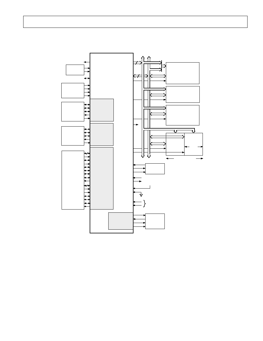
PCI Bus Mode
Figure 7 illustrates a typical system configuration for the
PCI mode.
REV. 0
ADSP-2141L
14
DEVICE OPERATION
OPERATIONAL MODES
Security Modes
The ADSP-2141L operates in one of two security modes: kernel
mode or user mode. The mode switching is performed on the fly
as program execution proceeds. Kernel mode is entered via a
jump or call to address 0x2000 with PMOVLAY set to 0x000F.
Kernel mode will exit on its own once it has completed a requested
operation (or terminates due to an error).
Special interrupt handling is performed if the DSP is executing
in kernel mode. While executing a CGX command in kernel
mode, it is possible to interrupt to a nonprotected vector loca-
tion and then invoke the kernel again during the interrupt han-
dler. The [IF CONDITION] RTI instruction must be used to
return to the kernel from the interrupt handler. The return
address and PMOVLAY page must match the interrupted ad-
dress and PMOVLAY page. If not, the violation reset logic will
be triggered. Only one level of kernel mode nesting is permitted.
An interrupt to a nonprotected vector location while in nested
kernel mode will also trigger the violation reset logic.
While in kernel mode, it is possible to interrupt to a protected
vector location. In this case, the processor remains in kernel
mode. The [IF CONDITION] RTI instruction must be used to
return the processor from the interrupt handler. There is no
imposed limit on the number of nested interrupts to a protected
vector location.
Bus Modes
The ADSP-2141L Host Bus may be configured for one of two
personalities: IDMA Mode or PCI Bus Mode. The selection of
mode is made with two hardware control inputs BUS_MODE
and BUS_SEL at boot time.
Table II. Bus Mode Selection
Bus Mode Pins
BUS_MODE
BUS_SEL
IDMA Mode
0
0
PCI Bus Mode
1
0
This selection may not be changed after the ADSP-2141L
comes out of power-up reset. It is typically expected that the bus
mode signals are tied to ground or VDD on the PC Board.
Boot Modes
The ADSP-2141L may be bootstrap-loaded from one of three
sources: byte-wide memory, host processor bus, or external
program memory. The selection of mode is made with two
hardware control inputs BMODE and MMAP. When the host
processor boot mode is selected, any one of the two bus modes
may be used.
Table III. Boot Mode Selection
Boot Mode Pins
BMODE
MMAP
Byte-Wide (BDMA) Boot Mode
0
0
Host Bus (IDMA) Boot Mode
1
0
External Program Boot Mode
0
1
The hardware pin states are not relevant after the ADSP-2141L
comes out of power-up reset. Refer to the ADSP-2141L User's
Manual (available from IRE) for information on BDMA, IDMA
and external program boot modes.
COMMAND INTERFACE
This section provides a general overview of the software com-
mand interface to the crypto functions in the ADSP-2141L.
Refer to the ADSP-2141 CGX Interface Programmer's Guide
(available from http://www.ire-ma.com/proddoc.htm) for more
details.
Overview
The ADSP-2141L provides an embedded crypto library that
provides a command interface API (Application Programming
Interface) to outside applications. These commands are referred
to as CGX (CryptoGraphic eXtensions).
The CGX API simultaneously enforces certain security policies
within the ADSP-2141L and insulates applications from the
details of many complex cryptographic operations. The security
policy built into the ADSP-2141L has some of the following
rules:
·
Unencrypted (red) keys may never be retrieved from the
ADSP-2141L.
·
Keys within the ADSP-2141L are marked with an attributes
field that specifies key type and trust level.
·
A key's type field must match the use in a requested opera-
tion (i.e., cannot use a KEK to encrypt traffic).
·
Keys generated internal to the ADSP-2141L (i.e., from RNG)
are marked as trusted.
·
Keys that are negotiated or imported from outside systems are
marked untrusted (although they may still be quite secure).
·
Separate trusted and untrusted key hierarchies may be main-
tained and customer applications may choose which trust
level is required for a given command.
For most key management operations, the CGX interface must
be used. However, for certain high performance encryption/
hashing applications, the CGX interface may be bypassed and
either the DSP or a host processor may exercise direct control
over the hash/encrypt block.

REV. 0
ADSP-2141L
15
COMMAND SUMMARY
Approximately 40 CGX Commands are supported in the API to the ADSP-2141L.
General Utilities
INIT
Initializes Secure Kernel and Allow Reconfiguration of the ADSP-2141L
DEFAULT
Restores Factory Default Settings
RANDOM
Generates Random Numbers (between 1K and 64K bytes)
GET CHIPINFO
Returns ADSP-2141L System Information
SELF TEST
Runs a suite of self-tests on the hardware and CGX
Symmetrical Key Management
UNCOVER KEY
Loads and Decrypts a Secret Key
GEN KEY
Generates a Secret Key
GEN KEK
Generates an Internal Key Encryption Key
GEN RKEK
Generates a Key Recovery Key Encryption Key
SAVE KEY
Saves a key protected by the Recovery Key (RKEK)
LOAD KEY
Imports a Red (plaintext) User Secret Key
DERIVE KEY
Derives a Secret Key from a Pass Phrase
TRANSFORM KEY
Transforms a Secret Key using IPsec
DESTROY KEY
Removes Secret Key from the KCR
EXPORT KEY
Exports an IRE-format Secret Key
IMPORT KEY
Imports an IRE-format Secret Key
Symmetrical Encryption
ENCRYPT
Encrypts Data
DECRYPT
Decrypts Data
LOAD KG
Loads Secret Key into HW/SW Key Generator
Hash
HASH INIT
Initializes the Hash Operator
HASH DATA
Hash Customer Data
HASH ENCRYPT
Hash and Encrypt Customer Data
HASH DECRYPT
Hash and Decrypt Customer Data
PRF Functions
MERGE KEY
Combines two secret keys into one key
MERGE LONG KEY
Combines two secret keys into a data string (long key)
EXTRACT LONG KEY
Creates a secret key from a data string (long key)
PRF DATA
Hash multiple data items using HMAC
PRF KEY
Completes the above HMAC and create secret key
Asymmetrical Key Management
GEN PUBKEY
Generates a Public Keyset (Public and Private Parts)
GEN NEWPUBKEY
Generates a part of a Public Keyset
GEN NEGKEY
Generates a Diffie-Hellman Derived Secret Key
EXPORT PUBKEY
Exports an IRE-format Public Key
IMPORT PUBKEY
Imports an IRE-format Public Key
Asymmetrical Encryption
PUBKEY ENCRYPT
Encrypts Data using RSA Public Key
PUBKEY DECRYPT
Decrypts Data using RSA Public Key
Digital Signatures
SIGN
Digitally Signs a Message
VERIFY
Verifies a Digital Signature
Math Utilities
ADD VECTOR
Performs a Vector Add Operation
SUB VECTOR
Performs a Vector Subtract Operation
MULT VECTOR
Performs a Vector Multiply Operation
EXP VECTOR
Performs a Vector Exponentiate Operation
SHIFT VECTOR
Performs a Vector Right or Left Shift Operation
Extended Mode
LOAD EXTENDED
Loads/Enables Extended (Downloaded) Algorithm Block
EXECUTE EXTENDED
Executes Extended (Downloaded) Algorithm Block

REV. 0
ADSP-2141L
16
ABSOLUTE MAXIMUM RATINGS
Supply Voltage . . . . . . . . . . . . . . . . . . . . . . . . 0.3 V to +4.6 V
Input Voltage . . . . . . . . . . . . . . . . . . . . 0.5 V to V
DD
+ 0.5 V
Output Voltage Swing . . . . . . . . . . . . . 0.5 V to V
DD
+ 0.5 V
Operating Temperature Range (Ambient) . . . . . 0
°
C to 70
°
C
Storage Temperature Range . . . . . . . . . . . . 65
°
C to +150
°
C
Lead Temperature (5 sec) MQFP . . . . . . . . . . . . . . . . . 280
°
C
CAUTION
ESD (electrostatic discharge) sensitive device. Electrostatic charges as high as 4000 V readily
accumulate on the human body and test equipment and can discharge without detection.
Although the ADSP-2141L features proprietary ESD protection circuitry, permanent damage
may occur on devices subjected to high energy electrostatic discharges. Therefore, proper ESD
precautions are recommended to avoid performance degradation or loss of functionality.
WARNING!
ESD SENSITIVE DEVICE
Frequency Dependency For Timing Specifications
t
CK
is defined as 0.5t
CKI
. The ADSP-2141L uses an input clock
with a frequency equal to half the instruction rate: a 20.0 MHz
input clock (which is equivalent to 50 ns) yields a 25 ns processor
cycle (equivalent to 40 MHz). t
CK
values within the range of 0.5t
CKI
period should be substituted for all relevant timing parameters to
obtain the specification value.
Example: t
CKH
= 0.5t
CK
7 ns = 0.5 (25 ns) 7 ns = 8 ns

REV. 0
17
RECOMMENDED OPERATING CONDITIONS
K Grade
Parameter
Min
Max
Unit
V
DD
Supply Voltage
3.0
3.6
V
T
AMB
Ambient Operating Temperature
0
70
°
C
ELECTRICAL CHARACTERISTICS
DC SPECIFICATIONS
K Grade
Parameter
Test Conditions
Min
Typ
Max
Unit
V
IH
Hi-Level Input Voltage
1, 2
@ V
DD
= max
2.0
V
V
IH
Hi-Level CLKIN/Reset Voltage
@ V
DD
= max
2.4
V
V
IL
Lo-Level Input Voltage
1, 3
@ V
DD
= min
0.4
V
V
OH
Hi-Level Output Voltage
1, 4, 5
@ V
DD
= min
I
OH
= 0.5 mA
2.4
V
@ V
DD
= min
I
OH
= 100
µ
A
6
V
DD
0.3
V
V
OL
Lo-Level Output Voltage
1, 4, 5
@ V
DD
= min
I
OL
= 2 mA
0.4
V
I
IH
Hi-Level Input Current
3
@ V
DD
= max
V
IN
= V
DD
max
10
µ
A
I
IL
Lo-Level Input Current
3
3 @ V
DD
= max
V
IN
= 0 V
10
µ
A
I
OZH
Three-State Leakage Current
7
@ V
DD
= max
V
IN
= V
DD
max
8
10
µ
A
I
OZL
Three-State Leakage Current
9
@ V
DD
= max
V
IN
= 0 V
9
8
µ
A
I
DD
Supply Current (Idle)
10, 11
@ V
DD
= 3.3
T
AMB
= 25
°
C
t
CK
= 25 ns
12
16
mA
t
CK
= 30 ns
12
15
mA
I
DD
Supply Current (Dynamic)
11, 13
@ V
DD
= 3.3
T
AMB
= 25
°
C
t
CK
= 25 ns
12
195
mA
t
CK
= 30 ns
12
165
mA
C
I
Input Pin Capacitance
3, 6, 14
@ V
IN
= 2.5 V
f
IN
= 1.0 MHz
T
AMB
= 25
°
C
8
pF
C
O
Output Pin Capacitance
6, 7, 14, 15
@ V
IN
= 2.5 V
f
IN
= 1.0 MHz
T
AMB
= 25
°
C
8
pF
NOTES
1
Bidirectional pins: D0D31, RFS0, RFS1, SCLK0, SCLK1, TFS0, TFS1, IAD015, PF0PF7.
2
Input only pins:
IRQ2, BR, MMAP, BMODE, BUS MODE, BUS SEL, DR0, DR1, PWD, IRQL0, IRQL1, IRQE, IS, IRD, IWR, IAL.
3
Input only pins: CLKIN,
RESET, IRQ2, BR, MMAP, BMODE, BUS MODE, BUS SEL, DR0, DR1, PWD, IRQL0, IRQL1, IRQE, IS, IRD, IWR, IAL.
4
Output pins:
BG, BGH, PMS, DMSL, DMSH, BMS, IOMS, CMS, RD, WR, IACK, PWDACK, A0A25, DT0, DT1, CLKOUT, FL20.
5
Although specified for TTL outputs, all ADSP-2141L outputs are CMOS-compatible and will drive to V
DD
and GND, assuming no dc loads.
6
Guaranteed but not tested.
7
Output pins:
BG, BGH, PMS, DMSL, BMS, IOMS, DMSH, CMS, RD, WR, IACK, PWDACK, A0A25, DT0, DT1, CLKOUT, FL20, EE_DI, EE_CS, EE_SK.
8
0 V on BR. CLKIN active (to force three-state condition).
9
Three-statable pins: A0A25, D0D31,
PMS, DMSL, DMSH, BMS, IOMS, CMS, RD, WR, DT0, DT1, SCKL0, SCLK1, TFS0, TFS1, RFS0, RFS1, IAD0
IAD15, PF0PF7.
10
Idle refers to ADSP-2141L state of operation during execution of IDLE Instruction. Deasserted pins are driven to either V
DD
or GND.
11
Current reflects device operating with no output loads.
12
V
IN
= 0.4 V and 2.4 V. For typical supply currents, refer to Power Dissipation section.
13
I
DD
measurement taken with 93% of instructions executing from internal memory and 7% from external memory. H/E operations are executing from internal
memory concurrently with PCI transactions. Initialization operations are executed from external memory.
14
Applies to MQFP package type.
15
Output pin capacitance is the capacitive load for any three-stated output pin.
Specifications subject to change without notice.
ADSP-2141L
SPECIFICATIONS
REV. 0
ADSP-2141L
18
DC SPECIFICATIONS PCI Bus Pins
K Grade
Parameter
Test Conditions
Min
Max
Unit
V
IH
Hi-Level Input Voltage
1, 2
0.5 V
DD
V
DD
+ 0.5
V
V
IL
Lo-Level Input Voltage
1, 2
0.5
0.3 V
DD
V
V
OH
Hi-Level Output Voltage
1, 3
I
OUT
= 500
µ
A
0.9 V
DD
V
V
OL
Lo-Level Output Voltage
1, 3
I
OUT
= 1500
µ
A
0.1 V
DD
V
I
IH
Hi-Level Input Current
2
0 < V
IN
< V
DD
10
µ
A
I
IL
Lo-Level Input Current
2
0 < V
IN
< V
DD
10
µ
A
I
OZH
Three-State Leakage Current
4
0 < V
IN
< V
DD
10
µ
A
I
OZL
Three-State Leakage Current
1
0 < V
IN
< V
DD
10
µ
A
C
I
Input Pin Capacitance
T
AMB
= 25
°
C
10
pF
C
CLK
PCI CLK Pin Capacitance
T
AMB
= 25
°
C
5
12
pF
C
IDSEL
PCI IDSEL Pin Capacitance
5
T
AMB
= 25
°
C
8
pF
L
PIN
Pin Inductance
20
nH
NOTES
1
Bidirectional pins: MPLX_BUS [31:0}, MPLX14, MPLX710, MPLX12
2
Input only pins: MPLX_RESET, MPLX5, MPLX6, PCI_CLK, PCI_PAR, PCI_IRDY, PCI_STOP
3
Output only pins: MPLX11
4
Leakage currents include High-Z output leakage for bidirectional buffers with three-state outputs.
5
Lower capacitance of IDSEL (MPLX_5) input-only pin allows for nonresistive connection to Address/Data bus.
TIMING PARAMETERS
PCI Clock
(Guaranteed Over Operating Temperature and Digital Supply Range)
The ADSP-2141L is targeted for use in PCI add-on I/O slave card designs. It provides a glueless interface to the PCI bus. All bus
drivers are compliant with PCI interface electrical switching and drive capability specifications.
The ADSP-2141L does not implement the following signals:
LOCK, INTB, INTC, INTD, SBO, SDONE, CLKRUN, AD[64:32],
C/BE[7:4], REQ64, ACK64, PAR64.
Parameter
Min
Max
Unit
Timing Requirements:
t
CYC
CLK Cycle Time
25
100
ns
t
HIGH
CLK High Time
11
ns
t
LOW
CLK Low Time
11
ns
CLK Slew Rate
1
1
4
V/ns
RST Slew Rate
2
50
mV/ns
NOTES
1
Rise and fall times are specified in terms of the edge rate measured in V/ns. This slew rate must be met across the minimum peak-to-peak portion of the waveform as
shown in Figure 8.
2
The minimum
RST slew rate applies only to the rising (deassertion) edge of the reset signal, and ensures that system noise cannot render an otherwise monotonic
signal to appear to bounce in the switching range.
0.2V
CC
2V p-p
(
MINIMUM
)
0.3V
CC
0.4V
CC
0.5V
CC
0.6V
CC
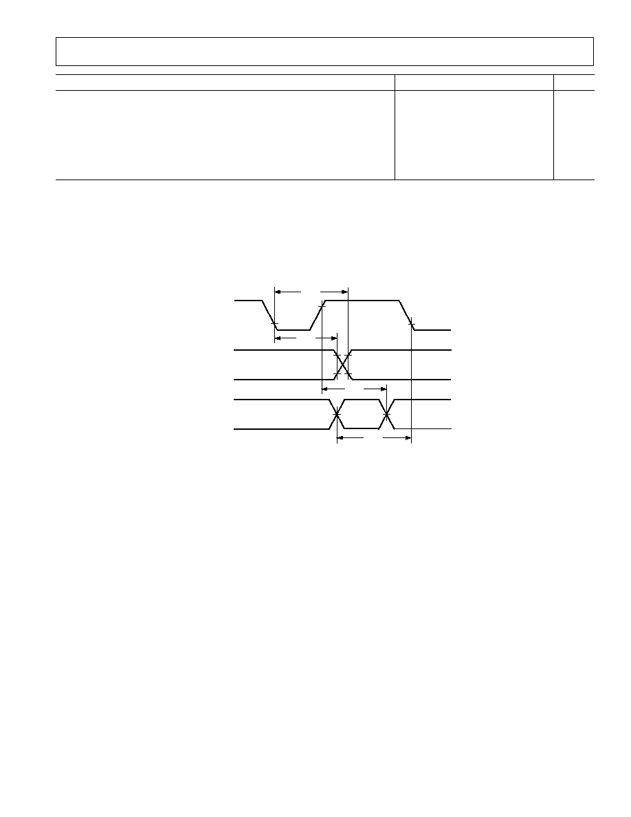
t
LOW
t
HIGH
t
CYC
Figure 8. Clock Waveform
REV. 0
ADSP-2141L
19
Parameter
Min
Max
Unit
PCI Bus Interface
Timing Requirements:
t
VAL
CLK to Signal Valid
2
11
ns
t
ON
CLK to Low-Z Delay
2
ns
t
OFF
CLK to High-Z Delay
28
ns
t
SU
Input Setup to CLK
7
ns
t
H
Input Hold After CLK
1
ns
t
RST-OFF
RST Active to Outputs High-Z
40
ns
V
STEP
(3.3V SIGNALING)
V
TL
V
TEST
V
TH
V
TEST
INPUTS
VALID
OUTPUT CURRENT LEAKAGE CURRENT
V
TEST
t
VAL
CLK
OUTPUT
DELAY
t
ON
t
OFF
THREE-STATE
OUTPUT
t
SU
t
H
V
MAX
V
TH
V
TL
CLK
INPUT
Figure 9. Output (Top) and Input Timing Measurement Conditions
REV. 0
ADSP-2141L
20
Parameter
Min
Max
Unit
Clock Signals and Reset
Timing Requirements:
t
CKI
CLKIN Period
50
100
ns
t
CKIL
CLKIN Width Low
15
ns
t
CKIH
CLKIN Width High
15
ns
Switching Characteristics:
t
CKL
CLKOUT Width Low
0.5t
CK
7
ns
t
CKH
CLKOUT Width High
0.5t
CK
7
ns
t
CKOH
CLKIN High to CLKOUT High
0
20
ns
Control Signals
Timing Requirement:
t
RSP
RESET Width Low
1
5t
CK
ns
NOTE
1
Applies after power-up sequence is complete. Internal phase lock loop requires no more than 2000 CLKIN cycles assuming stable CLKIN (not including crystal
oscillator start-up time).
t
CKIH
t
CKI
t
CKIL
t
CKOH
t
CKH
t
CKL
CLKIN
CLKOUT
Figure 10. Clock Signals and Reset
REV. 0
ADSP-2141L
21
Parameter
Min
Max
Unit
Interrupts and Flags
Timing Requirements:
t
IFS
IRQx, FI, or PFx Setup Before CLKOUT Low
1, 2, 3, 4
0.25t
CK
+ 15
ns
t
IFH
IRQx, FI, or PFx Hold After CLKOUT High
1, 2, 3, 4
0.25t
CK
ns
Switching Characteristics:
t
FOH
Flag Output Hold After CLKOUT Low
5
0.5t
CK
7
ns
t
FOD
Flag Output Delay from CLKOUT Low
5
0.5t
CK
+ 5
ns
NOTES
1
If
IRQx and FI inputs meet t
IFS
and t
IFH
setup/hold requirements, they will be recognized during the current clock cycle; otherwise the signals will be recognized on
the following cycle. (Refer to the Interrupt Controller Operation section in the Program Control chapter of the ADSP-2100 Family User's Manual for further informa-
tion on interrupt servicing.)
2
Edge-sensitive interrupts require pulsewidths greater than 10 ns; level-sensitive interrupts must be held low until serviced.
3
IRQx = IRQ0, IRQ1, IRQ2, IRQL0, IRQL1, IRQE.
4
PFx = PF0, PF1, PF2, PF3, PF4, PF5, PF6, PF7.
5
Flag Outputs = PFx, FL0, FL1, FL2, Flag_out.
t
FOD
t
FOH
t
IFH
t
IFS
CLKOUT
FLAG
OUTPUTS
IRQx
FI
PFx
Figure 11. Interrupts and Flags
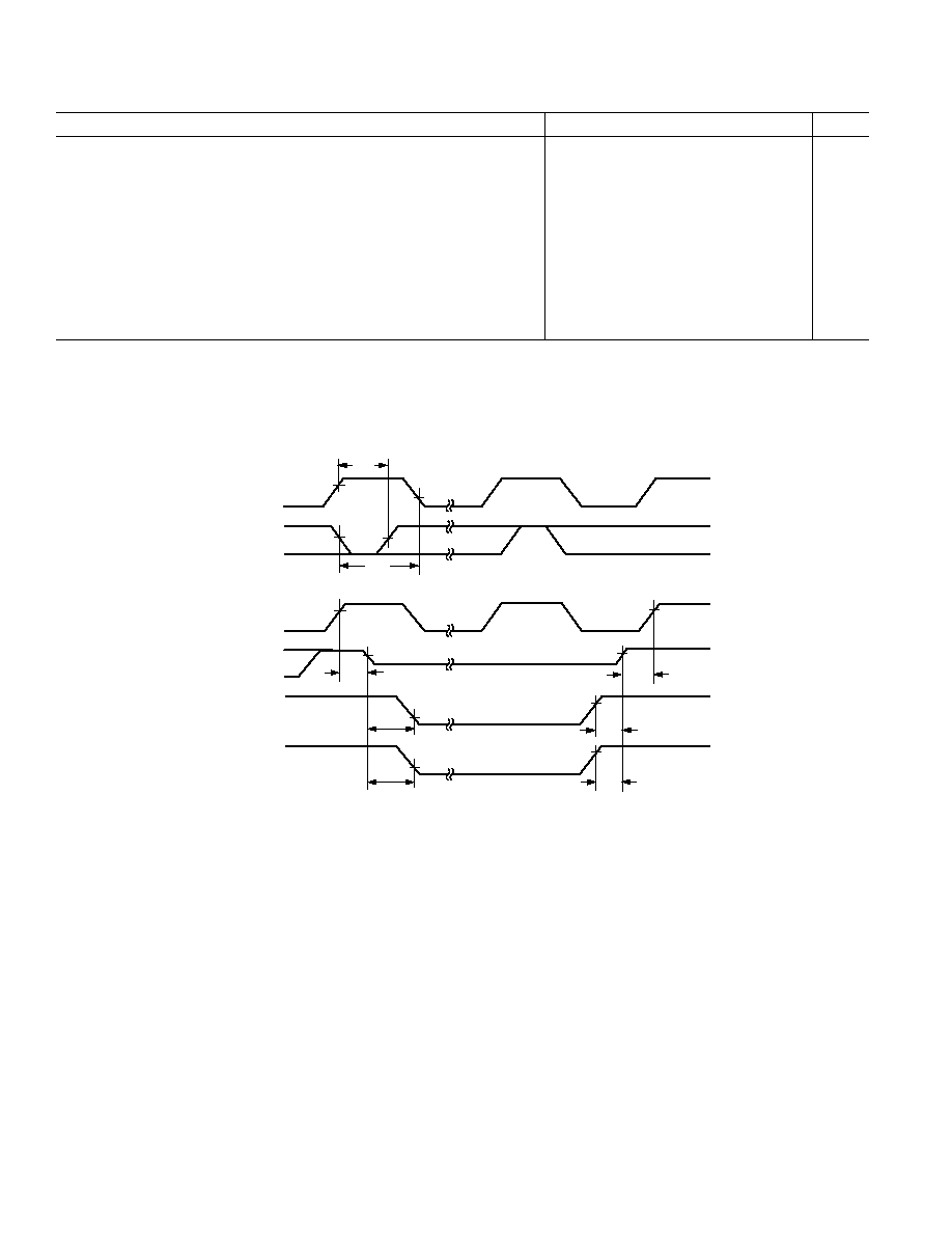
REV. 0
ADSP-2141L
22
Parameter
Min
Max
Unit
Bus Request/Bus Grant
Timing Requirements:
t
BH
BR Hold After CLKOUT High
1
0.25t
CK
+ 2
ns
t
BS
BR Setup Before CLKOUT Low
1
0.25t
CK
+ 17
ns
Switching Characteristics:
t
SD
CLKOUT High to
xMS, RD, WR Disable
0.25t
CK
+ 10
ns
t
SDB
xMS, RD, WR Disable to BG Low
0
ns
t
SE
BG High to
xMS, RD, WR Enable
0
ns
t
SEC
xMS, RD, WR Enable to CLKOUT High
0.25t
CK
6
ns
t
SDBH
xMS, RD, WR Disable to BGH Low
2
0
ns
t
SEH
BGH High to xMS, RD, WR Enable
2
0
ns
NOTES
xMS = PMS, DMSL, DMSH, CMS, IOMS, BMS.
1
BR is an asynchronous signal. If BR meets the setup/hold requirements, it will be recognized during the current clock cycle; otherwise, the signal will be recognized
on the following cycle. Refer to the ADSP-2100 Family User's Manual for
BR/BG cycle relationships.
2
BGH is asserted when the bus is granted and the processor requires control of the bus to continue.
t
BH
t
BS
t
SD
t
SDB
t
SDBH
CLKOUT
BR
CLKOUT
PMS
,
DMSL
,
BMS
,
RD
,
WR
BG
BGH
t
SEC
t
SE
t
SEH
Figure 12. Bus Request/Bus Grant
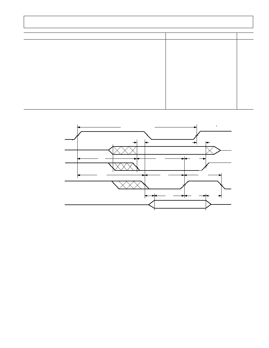
REV. 0
ADSP-2141L
23
Parameter
Min
Max
Unit
External Memory Write: ADSP-2141L DMA Initiated
Switching Characteristics:
t
A
Clock to Address and
DMSx
5
9
ns
t
DW
Data Setup Before Write Deasserted
0.5t
CK
2 + w
ns
t
DH
Data Hold After Write Deasserted
0.5t
CK
8
ns
t
WP
Write Pulsewidth
0.5t
CK
5 + w
ns
t
WDE
Write Low to Data Enabled
5
ns
t
ASW
Address,
DMSx Setup Before Write Low
1
ns
t
DDR
Data Disable Before Write/Read Low
0
ns
t
CWR
Clock High to Write Low
6
12
ns
t
AW
Address,
DMSx Setup Before Write High
0.5t
CK
2 + w
ns
t
AH
Address and
DMSx Hold After Clock
2
ns
t
WRA
Address,
DMSx Hold After Write High
0.5t
CK
7
ns
t
WWR
Write High to Read/Write Low
0.5t
CK
3
ns
1. If wait-state(s) added, then referenced to last wait-state clock interval.
2. w = DMA wait states
×
t
CK
.
t
AH
25ns (REF @ 40MHz)
t
ASW
t
A
t
AW
t
WRA
t
WWR
t
CWR
t
WP
t
WDE
t
DW
t
DH
t
DDR
DSP CLOCK
OUT
EXT. ADDR
(A250)
EXT.
DMSH
EXT.
DMSL
EXT.
WR
EXT. DATA
(D310)
Figure 13. External Memory Write: ADSP-2141L DMA Initiated
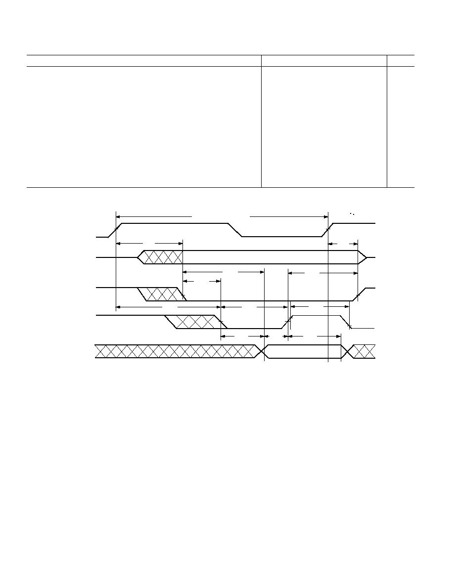
REV. 0
ADSP-2141L
24
Parameter
Min
Max
Unit
External Memory Read--ADSP-2141L DMA Initiated
Timing Requirements:
t
RDD
Read Low to Data Valid
0.5t
CK
8 + w
ns
t
AA
Address,
DMSx Valid to Data Valid
0.5t
CK
3 + w
ns
t
SUR
Data Valid Before Read Deasserted
4
ns
t
RDH
Data Hold After Read Deasserted
1
ns
Switching Characteristics:
t
A
Clock to Address and
DMSx Active
5
9
ns
t
ASR
Address,
DMSx Setup Before Read Low
2
ns
t
AH
Address and
DMSx Hold After Clock
2
ns
t
RDA
Address,
DMSx Hold After Read High
0.5t
CK
7
ns
t
CRD
Clock High to
RD Low
8
12
ns
t
RP
Read Pulsewidth
0.5t
CK
5 + w
ns
t
RWR
RD High to Read or Write Low
0.5t
CK
3
ns
1. If wait-state(s) added, then referenced to last wait-state clock interval.
2. w = DMA wait states
×
t
CK
.
25ns (REF @ 40MHz)
t
A
t
AA
t
RDD
DSP CLOCK
OUT
EXT. ADDR
(A250)
EXT.
DMSH
EXT.
DMSL
EXT.
RD
EXT. DATA
(D310)
t
AH
t
RDA
t
ASR
t
CRD
t
RP
t
SUR
t
RDH
t
RWR
Figure 14. External Memory Read ADSP-2141L DMA Initiated
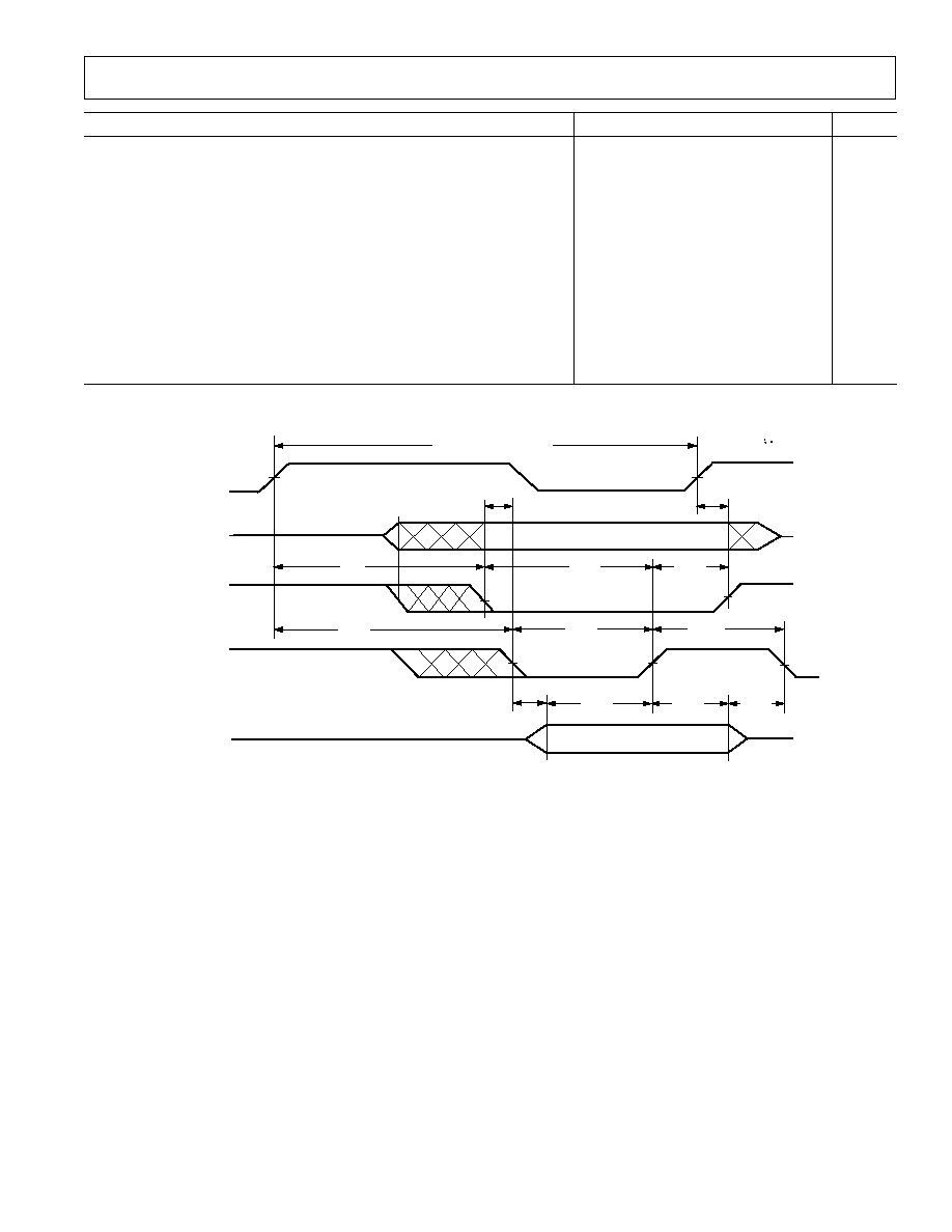
REV. 0
ADSP-2141L
25
Parameter
Min
Max
Unit
External Memory Write: ADSP-2141L DSP Initiated
Switching Characteristics:
t
A
Clock to Address,
xMS
1
6
ns
t
DW
Data Setup Before Write Deasserted
0.5t
CK
7 + w
ns
t
DH
Data Hold After Write Deasserted
0.25t
CK
3.5
ns
t
WP
Write Pulsewidth
0.5t
CK
5 + w
ns
t
WDE
Write Low to Data Enabled
0
ns
t
ASW
Address,
xMS Setup Before Write Low
0.25t
CK
4
ns
t
DDR
Data Disable Before Write/Read Low
0.25t
CK
4
ns
t
CWR
Clock High to Write Low
0.25t
CK
0.5t
CK
+ 9
ns
t
AW
Address,
xMS Setup Before Write High
0.75t
CK
6 + w
ns
t
AH
Address,
xMS Hold After Clock
1
ns
t
WRA
Address,
xMS Hold After Write High
0.25t
CK
4
ns
t
WWR
Write High to Read/Write Low
0.5t
CK
5
ns
1. If wait-state(s) added, then referenced to last wait-state clock interval.
2. w = DSP wait states
×
t
CK .
t
AW
DSP CLOCK
OUT
EXT. ADDR
(A130)
EXT.
WR
EXT. DATA
(D230)
t
AH
t
WRA
t
ASW
t
WP
25ns (REF @ 40MHz)
t
A
t
CWR
t
WWR
t
WDE
t
DW
t
DH
t
DDR
PMS
,
DMSx
,
BMS
,
IOMS
,
CMS
Figure 15. External Memory Write: ADSP-2141L DSP Initiated
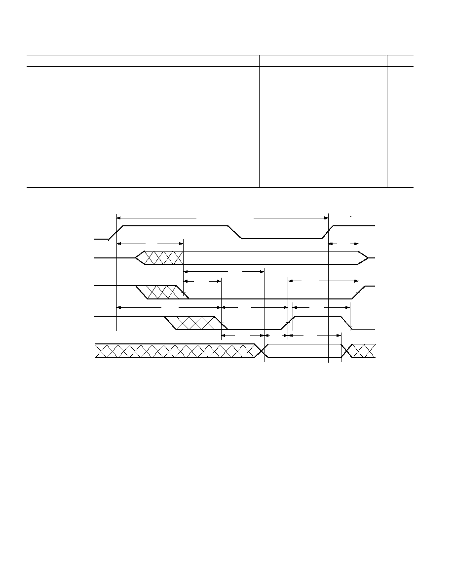
REV. 0
ADSP-2141L
26
Parameter
Min
Max
Unit
External Memory Read--ADSP-2141L DSP Initiated
Timing Requirements:
t
RDD
Read Low to Data Valid
0.5t
CK
10 + w
ns
t
AA
Address,
xMS Valid to Data Valid
0.75t
CK
11.5 + w
ns
t
SUR
Data Valid Before Read Deasserted
9
ns
t
RDH
Data Hold After Read Deasserted
0
ns
Switching Characteristics:
t
A
Clock to Address,
xMS Active
1
6
ns
t
ASR
Address,
xMS Setup Before Read Low
0.25t
CK
4
ns
t
AH
Address,
xMS Hold After Clock
1
ns
t
RDA
Address,
xMS Hold After Read High
0.25t
CK
3
ns
t
CRD
Clock High to
RD Low
0.25t
CK
2
0.25t
CK
+ 7
ns
t
RP
Read Pulsewidth
0.5t
CK
5 + w
ns
t
RWR
RD High to
RD or WR Low
0.5t
CK
5
ns
1. If wait-state(s) added, then referenced to last wait-state clock interval.
2. w = DSP wait state
×
t
CK
.
DSP CLOCK
OUT
EXT. ADDR
(A130)
EXT. RD
EXT. DATA
(D230)
t
AA
25ns (REF @ 40MHz)
t
RDA
t
CRD
t
AH
t
ASR
PMS
,
DMSx
,
BMS
,
IOMS
,
CMS
t
A
t
RP
t
SUR
t
RDD
t
RDH
t
RWR
Figure 16. External Memory Read ADSP-2141L DSP Initiated
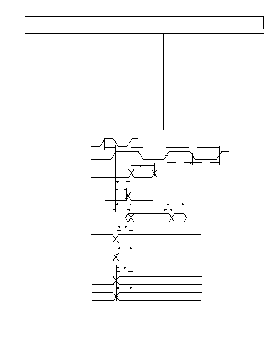
REV. 0
ADSP-2141L
27
Parameter
Min
Max
Unit
Serial Ports
Timing Requirements:
t
SCK
SCLK Period
50
ns
t
SCS
DR/TFS/RFS Setup Before SCLK Low
4
ns
t
SCH
DR/TFS/RFS Hold After SCLK Low
7
ns
t
SCP
SCLK
IN
Width
15
ns
Switching Characteristics:
t
CC
CLKOUT High to SCLKOUT
0.25t
CK
0.25t
CK
+ 10
ns
t
SCDE
SCLK High to DT Enable
0
ns
t
SCDV
SCLK High to DT Valid
15
ns
t
RH
TFS/RFS
OUT
Hold After SCLK High
0
ns
t
RD
TFS/RFS
OUT
Delay from SCLK High
15
ns
t
SCDH
DT Hold After SCLK High
0
ns
t
TDE
TFS (Alt) to DT Enable
0
ns
t
TDV
TFS (Alt) to DT Valid
14
ns
t
SCDD
SCLK High to DT Disable
15
ns
t
RDV
RFS (Multichannel, Frame Delay Zero) to DT Valid
15
ns
CLKOUT
t
CC
t
SCH
t
CC
t
SCK
t
SCP
t
SCP
t
SCS
t
RD
t
RH
t
SCDV
t
SCDD
t
SCDH
t
SCDE
t
TDE
t
TDV
t
RDV
t
TDE
t
TDV
t
RDV
SCLK
DR
TFS
IN
RFS
IN
RFS
OUT
TFS
OUT
DT
TFS
OUT
ALTERNATE
FRAME MODE
RFS
OUT
MULTICHANNEL MODE
FRAME DELAY 0
(MFD = 0)
TFS
IN
ALTERNATE
FRAME MODE
RFS
IN
MULTICHANNEL MODE
FRAME DELAY 0
(MFD = 0)
Figure 17. Serial Ports
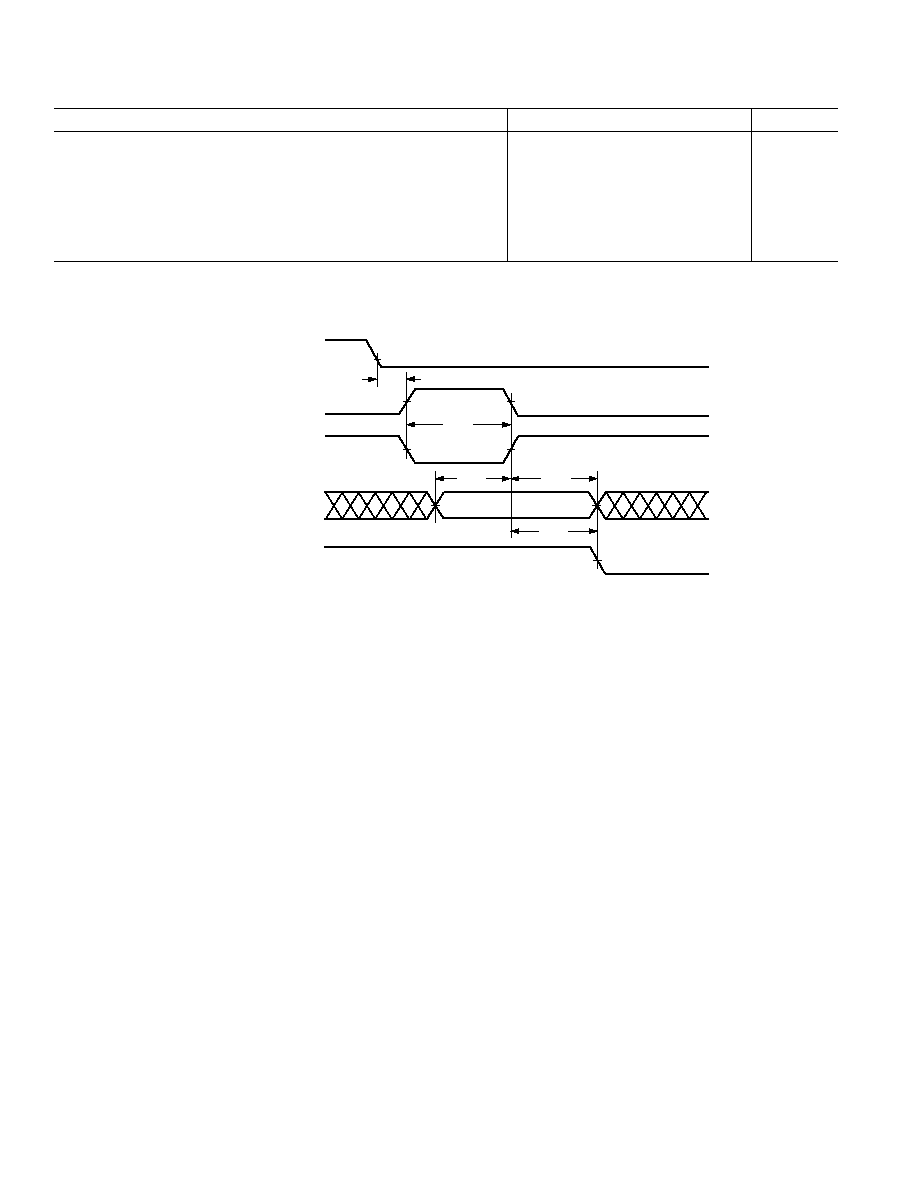
REV. 0
ADSP-2141L
28
Parameter
Min
Max
Unit
IDMA Address Latch (IDMA Mode Multiplex Bus)
Timing Requirements:
t
IALP
Duration of Address Latch
1, 2
10
ns
t
IASU
MPLX_BUS Address Setup Before Address Latch End
2
5
ns
t
IAH
MPLX_BUS Address Hold After Address Latch End
2
3
ns
t
IKA
MPLX9 Low Before Start of Address Latch
2, 3
0
ns
t
IALS
Start of Write or Read After Address Latch End
2, 3
4
ns
NOTES
1
Start of Address Latch = MPLX7 Low and MPLX8 High.
2
Start of Write or Read = MPLX7 Low and MPLX6 Low or MPLX5 Low.
3
End of Address Latch = MPLX7 High or MPLX8 Low.
t
IKA
t
IALP
t
IASU
t
IAH
t
IALS
MPLX9
/
IACK
MPLX8
/
IAL
MPLX7
/
IS
MPLX_BUS
/
IAD150
MPLX5 OR MPLX6
/
IRD
OR
IWR
Figure 18. IDMA Address Latch (IDMA Mode Multiplex Bus)
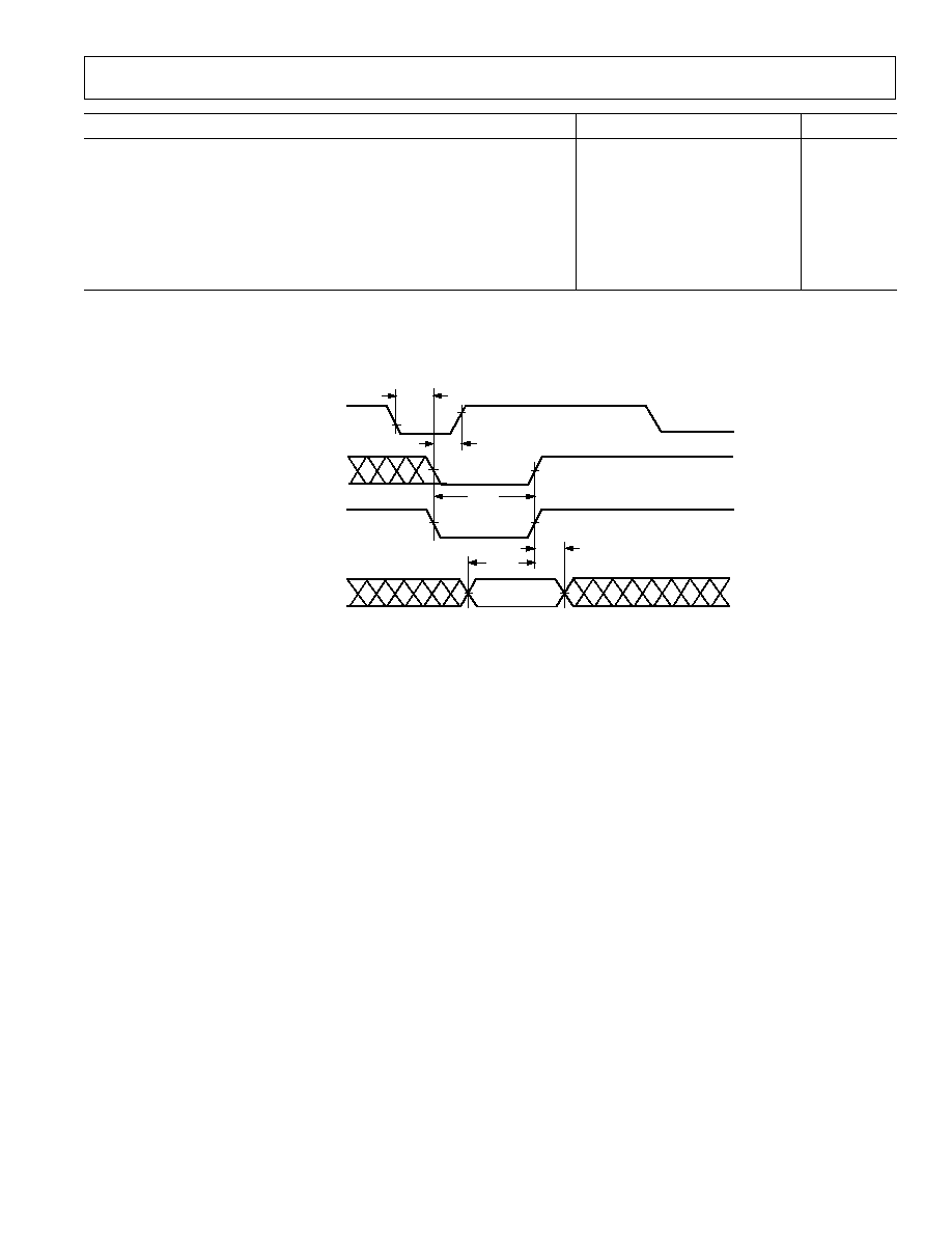
REV. 0
ADSP-2141L
29
Parameter
Min
Max
Unit
IDMA Write, Short Write Cycle (IDMA Mode, Multiplex Bus)
Timing Requirements:
t
IKW
MPLX9 Low Before Start of Write
1
0
ns
t
IWP
Duration of Write
1, 2
15
ns
t
IDSU
MPLX_BUS Data Setup Before End of Write
2, 3, 4
5
ns
t
IDH
MPLX_BUS Hold After End of Write
2, 3, 4
3
ns
Switching Characteristic:
t
IKHW
Start of Write to MPLX9 High
15
ns
NOTES
1
Start of Write = MPLX7 Low and MPLX6 Low.
2
End of Write = MPLX7 High or MPLX6 High.
3
If Write Pulse ends before MPLX9 Low, use specifications t
IDSU
, t
IDH
.
4
If Write Pulse ends after MPLX9 Low, use specifications t
IKSU
, t
IKH.
DATA
t
IKW
t
IKHW
MPLX9
/
IACK
MPLX7
/
IS
MPLX_BUS
/
IAD150
t
IWP
t
IDH
t
IDSU
MPLX6
/
IWR
Figure 19. IDMA Write, Short Write Cycle (IDMA Mode, Multiplex Bus)
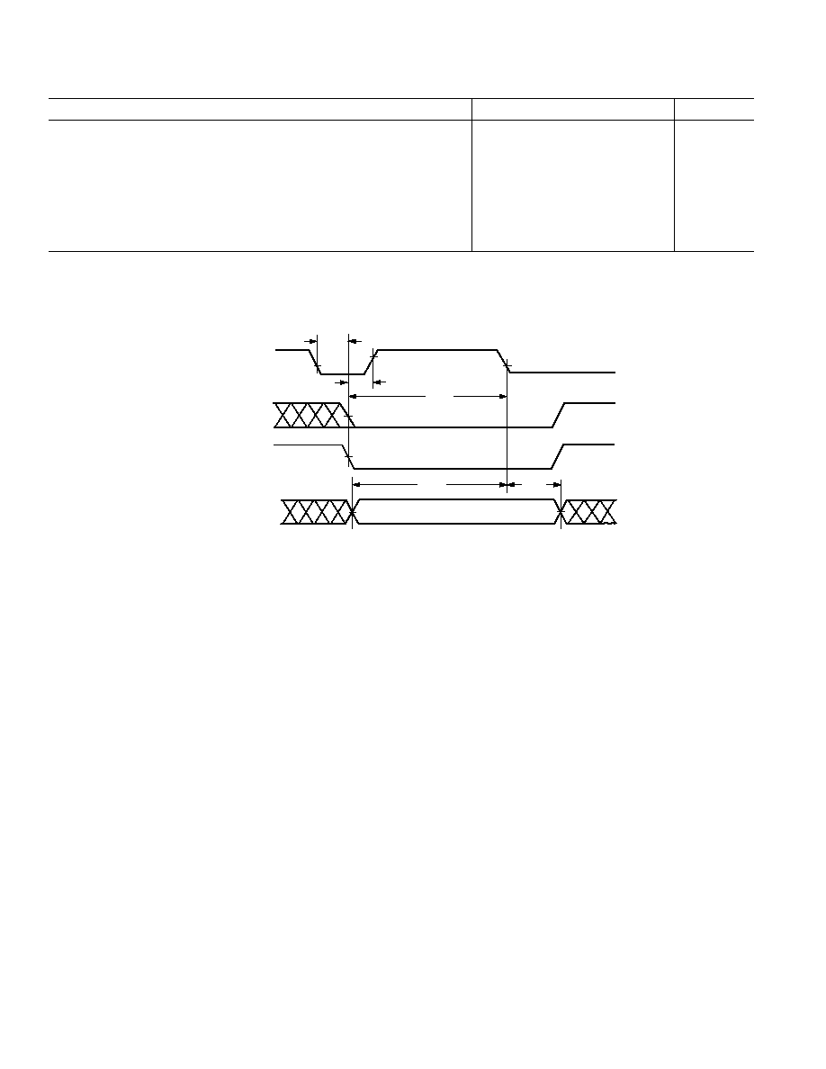
REV. 0
ADSP-2141L
30
Parameter
Min
Max
Unit
IDMA Write, Long Write Cycle (IDMA Mode, Multiplex Bus)
Timing Requirements:
t
IKW
MPLX9 Low Before Start of Write
1
0
ns
t
IKSU
MPLX_BUS Data Setup Before MPLX9 Low
2, 3, 4
0.5t
CK
+ 10
ns
t
IKH
MPLX_BUS Data Hold After MPLX9 Low
2, 3, 4
2
ns
Switching Characteristics:
t
IKLW
Start of Write to MPLX9 Low
4
1.5t
CK
ns
t
IKHW
Start of Write to MPLX9 High
15
ns
NOTES
1
Start of Write = MPLX7 Low and MPLX6 Low.
2
If Write Pulse ends before MPLX9 Low, use specifications t
IDSU
, t
IDH.
3
If Write Pulse ends after MPLX9 Low, use specifications t
IKSU
, t
IKH.
4
This is the earliest time for MPLX9 Low from Start of Write. For IDMA Write cycle relationships, please refer to the ADSP-2100 Family User's Manual.
t
IKW
t
IKLW
MPLX9
/
IACK
MPLX7
/
IS
MPLX_BUS
/
IAD150
t
IKHW
t
IKSU
t
IKH
DATA
MPLX6
/
IWR
Figure 20. IDMA Write, Long Write Cycle (IDMA Mode, Multiplex Bus)
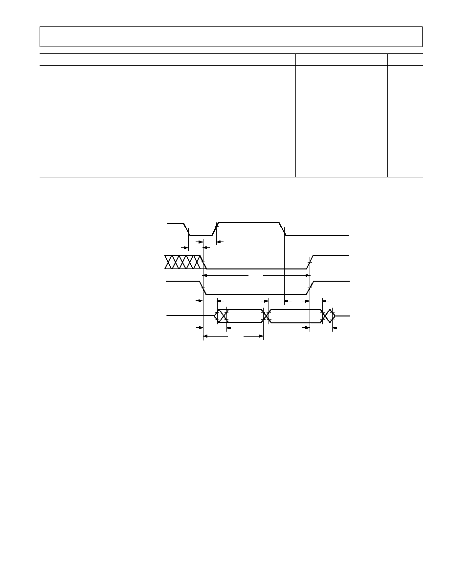
REV. 0
ADSP-2141L
31
Parameter
Min
Max
Unit
IDMA Read, Long Read Cycle (IDMA Mode, Multiplex Bus)
Timing Requirements:
t
IKR
MPLX9 Low Before Start of Read
1
0
ns
t
IRP
Duration of Read
1
15
ns
Switching Characteristics:
t
IKHR
MPLX9 High After Start of Read
1
15
ns
t
IKDS
MPLX_BUS Data Setup Before MPLX9 Low
0.5t
CK
7
ns
t
IKDH
MPLX_BUS Data Hold After End of Read
2
0
ns
t
IKDD
MPLX_BUS Data Disabled After End of Read
2
14
ns
t
IRDE
MPLX_BUS Previous Data Enabled After Start of Read
0
ns
t
IRDV
MPLX_BUS Previous Data Valid After Start of Read
15
ns
t
IRDH1
MPLX_BUS Previous Data Hold After Start of Read (DM/PM1)
3
2t
CK
5
ns
t
IRDH2
MPLX_BUS Previous Data Hold After Start of Read (PM2)
4
t
CK
5
ns
NOTES
1
Start of Read = MPLX7 Low and MPLX5 Low.
2
End of Read = MPLX7 High or MPLX5 High.
3
DM read or first half of PM read.
4
Second half of PM read.
t
IKHR
MPLX9
/
IACK
MPLX7
/
IS
MPLX_BUS
/
IAD150
t
IKR
t
IRP
t
IKDH
t
IKDS
t
IRDE
PREVIOUS
DATA
READ DATA
t
IRDV
t
IKDD
t
IRDH
MPLX6
/
IRD
Figure 21. IDMA Read, Long Read Cycle (IDMA Mode, Multiplex Bus)
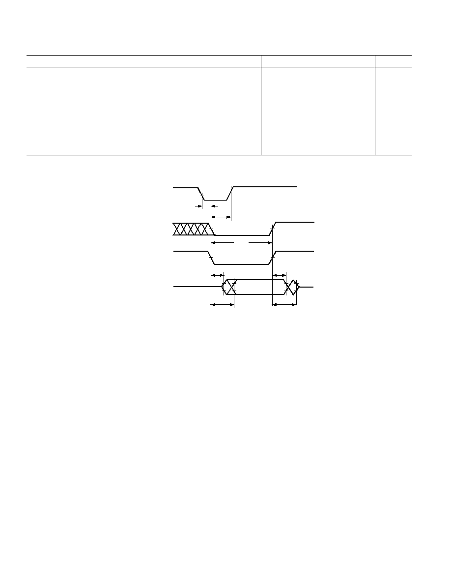
REV. 0
ADSP-2141L
32
Parameter
Min
Max
Unit
IDMA Read, Short Read Cycle (IDMA Mode, Multiplex Bus)
Timing Requirements:
t
IKR
MPLX9 Low Before Start of Read
1
0
ns
t
IRP
Duration of Read
15
ns
Switching Characteristics:
t
IKHR
MPLX9 High After Start of Read
1
15
ns
t
IKDH
MPLX_BUS Data Hold After End of Read
2
0
ns
t
IKDD
MPLX_BUS Data Disabled After End of Read
2
14
ns
t
IRDE
MPLX_BUS Previous Data Enabled After Start of Read
0
ns
t
IRDV
MPLX_BUS Previous Data Valid After Start of Read
15
ns
NOTES
1
Start of Read = MPLX7 Low and MPLX5 Low.
2
End of Read = MPLX7 High or MPLX5 High.
MPLX_BUS/IAD150
MPLX6/
IRD
MPLX7/
IS
MPLX9/
IACK
t
IKR
t
IKHR
t
IRP
t
IRDE
t
IKDH
PREVIOUS
DATA
t
IRDV
t
IKDD
Figure 22. IDMA Read, Short Read Cycle (IDMA Mode, Multiplex Bus)
REV. 0
ADSP-2141L
33
CAPACITIVE LOADING
Figures 23 and 24 show the capacitive loading characteristics of
the ADSP-2141L.
C
L
pF
RISE TIME (0.4V 2.4V) ns
0
50
18
14
T = +70 C
V
DD
= 3.0V
16
12
10
8
6
4
2
0
100
150
200
250
300
Figure 23. Typical Output Rise Time vs. Load Capacitance,
C
L
(at Maximum Ambient Operating Temperature)
C
L
pF
18
2
0
250
50
100
150
200
16
10
6
2
NOMINAL
14
12
8
4
4
VALID OUTPUT DELAY
OR HOLD ns
Figure 24. Typical Output Valid Delay or Hold vs. Load
Capacitance, C
L
(at Maximum Ambient Operating
Temperature)
TEST CONDITIONS
Output Disable Time
Output pins are considered to be disabled when they have
stopped driving and started a transition from the measured
output high or low voltage to a high impedance state. The out-
put disable time (t
DIS
) is the difference of t
MEASURED
and t
DECAY
,
as shown in the Output Enable/Disable diagram. The time is the
interval from when a reference signal reaches a high or low
voltage level to when the output voltages have changed by 0.5 V
from the measured output high or low voltage. The decay time,
t
DECAY
, is dependent on the capacitive load, C
L
, and the current
load, i
L
, on the output pin. It can be approximated by the fol-
lowing equation:
t
DECAY
=
C
L
· 0.5V
i
L
from which
t
DIS
=
t
MEASURED
t
DECAY
is calculated. If multiple pins (such as the data bus) are disabled,
the measurement value is that of the last pin to stop driving.
1.5V
INPUT
OR
OUTPUT
1.5V
Figure 25. Voltage Reference Levels for AC Measure-
ments (Except Output Enable/Disable)
Output Enable Time
Output pins are considered to be enabled when they have made
a transition from a high-impedance state to when they start
driving. The output enable time (t
ENA
) is the interval from when
a reference signal reaches a high or low voltage level to when the
output has reached a specified high or low trip point, as shown
in the Output Enable/Disable diagram. If multiple pins (such as
the data bus) are enabled, the measurement value is that of the
first pin to start driving.
2.0V
1.0V
t
ENA
REFERENCE
SIGNAL
OUTPUT
t
DECAY
V
OH
(MEASURED)
OUTPUT STOPS
DRIVING
OUTPUT STARTS
DRIVING
t
DIS
t
MEASURED
V
OL
(MEASURED)
V
OH
(MEASURED) 0.5V
V
OL
(MEASURED) +0.5V
HIGH-IMPEDANCE STATE. TEST CONDITIONS CAUSE
THIS VOLTAGE LEVEL TO BE APPROXIMATELY 1.5V.
V
OH
(MEASURED)
V
OL
(MEASURED)
Figure 26. Output Enable/Disable
TO
OUTPUT
PIN
50pF
+1.5V
I
OH
I
OL
Figure 27. Equivalent Device Loading for AC Measure-
ments (Including All Fixtures)
REV. 0
ADSP-2141L
34
Table IV. Thermal Ratings: MQFP Package
Rating Description
Symbol
Value (MQFP Still Air)
Value (MQFP 9500 fpm)
Thermal Resistance (Case to Ambient)
CA
30.7
°
C/W
16.7
°
C/W
Thermal Resistance (Junction to Ambient)
JA
35
°
C/W
21
°
C/W
Thermal Resistance (Junction to Case)
JC
4.3
°
C/W
4.3
°
C/W
ENVIRONMENTAL CONDITIONS
The following figures assume a four-layer JEDEC printed circuit
board:
T
AMB
= T
CASE
(PD
×
CA
)
T
CASE
= Case Temperature in
°
C
OUTPUT DRIVE CURRENTS
Figures 28 and 29 show typical I-V characteristics for the
output drivers of the ADSP-2141L. The curves represent the
current drive capability of the output drivers as a function of
output voltage.
SOURCE VOLTAGE V
100
40
100
0
3.5
SOURCE CURRENT mA
0.5
1.0
1.5
2.0
2.5
3.0
80
20
60
80
40
0
60
20
V
DD
= 3.0V @ +70 C
4.0
V
DD
= 3.3V @ +25 C
V
DD
= 3.6V @ 0 C
V
DD
= 3.0V @ +70 C
V
DD
= 3.3V @ +25 C
V
DD
= 3.6V @ 0 C
Figure 28. Typical Drive Currents (PCI Pins)
SOURCE VOLTAGE V
40
0
3.5
SOURCE CURRENT mA
0.5
1.0
1.5
2.0
2.5
3.0
80
20
60
80
40
0
60
20
V
DD
= 3.0V @ +70 C
4.0
V
DD
= 3.3V @ +25 C
V
DD
= 3.6V @ 0 C
V
DD
= 3.0V @ +70 C
V
DD
= 3.3V @ +25 C
V
DD
= 3.6V @ 0 C
V
OH
V
OL
Figure 29. Typical Drive Currents (Addr/Dbus/rd/wr Pins)
POWER DISSIPATION
Total power dissipation has two components: one due to inter-
nal circuitry and one due to the switching of external output
drivers. Internal power dissipation depends on the sequence in
which instructions execute and the data operands involved. See
I
DDIN
calculation in Electrical Characteristics section. Internal
power dissipation is calculated this way:
P
INT
= I
DDIN
×
V
DD
The external component of total power dissipation is caused by
the switching of output pins. Its magnitude depends on:
the number of output pins that switch during each cycle (O)
the maximum frequency at which the pins can switch (f)
the load capacitance of the pins (C)
the voltage swing of the pins (V
DD
).
The external component is calculated using:
P
EXT
= O
×
C
×
V
DD
2
×
f
The load capacitance should include the processor's package
capacitance (C
IN
). The frequency f includes driving the load
high and then back low.
REV. 0
ADSP-2141L
35
Example:
In an application where external data memory is used and no
other outputs are active, power dissipation is calculated as
follows:
Assumptions:
·
External data memory is accessed every cycle with 50% of the
address pins switching.
·
External data memory writes occur every other cycle with
50% of the data pins switching.
·
Each address and data pin has a 10 pF total load at the pin.
·
The application operates at V
DD
= 3.3 V and t
CK
= 25 ns.
Total Power Dissipation = P
INT
+ (C
×
V
DD
2
×
f )
P
INT
= internal power dissipation from Power vs. Frequency
graphs (Figures 30 and 31).
(C
×
V
DD
2
×
f ) is calculated for each output:
# of
Pins
×
C
×
V
DD
2
×
f
Address,
DMS
8
×
10 pF
×
3.3
2
V
×
40 MHz
=
34.8 mW
Data Output,
WR 9
×
10 pF
×
3.3
2
V
×
20 MHz
=
19.6 mW
RD
1
×
10 pF
×
3.3
2
V
×
40 MHz
=
2.2 mW
CLKOUT
1
×
10 pF
×
3.3
2
V
×
20 MHz
=
4.4 mW
61.0 mW
Total power dissipation for this example is P
INT
+61 mW.
FREQUENCY MHz
940
40
POWER (P
INT
) mW
33
34
35
36
37
38
840
340
640
440
740
540
42
32
41
39
V
DD
= 3.6V
V
DD
= 3.3V
V
DD
= 3.0V
706mW
554mW
431mW
823mW
649mW
509mW
POWER, INTERNAL
Figure 30. Power vs. Frequency
FREQUENCY MHz
80
40
POWER (P
IDLE
) mW
33
34
35
36
37
38
75
40
65
50
70
60
42
32
41
39
V
DD
= 3.6V
V
DD
= 3.3V
V
DD
= 3.0V
68mW
51mW
41mW
74mW
53mW
43mW
55
45
POWER, IDLE
Figure 31. Power vs. Frequency

REV. 0
ADSP-2141L
36
Pin Configurations
For all multiplexed pins the active sense is determined by the mode selected.
Pin # Pin Name
Pin # Pin Name
Pin # Pin Name
Pin # Pin Name
Pin #
Pin Name
1
EMS
43
PCI_CLK
85
VDD
127
GND
169
GND
2
EE
44
GND
86
GND
128
ADDR[0]
170
DATA[0]
3
GND
45
MPLX_BUS[30]
87
MPLX6
129
ADDR[1]
171
DATA[1]
4
ECLK
46
MPLX_BUS[29]
88
MPLX5
130
ADDR[2]
172
DATA[2]
5
ELOUT
47
MPLX_BUS[28]
89
MPLX_BUS[15]
131
ADDR[3]
173
DATA[3]
6
ELIN
48
MPLX_BUS[27]
90
MPLX_BUS[14]
132
VDD
174
VDD
7
EINT
49
VDD
91
MPLX_BUS[13]
133
ADDR[4]
175
GND
8
EBR
50
GND
92
MPLX_BUS[12]
134
ADDR[5]
176
DATA[4]
9
EBG
51
MPLX_BUS[26]
93
VDD
135
ADDR[6]
177
DATA[5]
10
MMAP
52
MPLX_BUS[25]
94
GND
136
ADDR[7]
178
DATA[6]
11
BMODE
53
MPLX_BUS[24]
95
MPLX_BUS[11]
137
ADDR[8]
179
DATA[7]
12
BUS_MODE
54
MPLX1
96
MPLX_BUS[10]
138
ADDR[9]
180
DATA[8]
13
BUS_SEL
55
MPLX_BUS[23]
97
MPLX_BUS[9]
139
ADDR[10]
181
DATA[9]
14
EE_SK
56
MPLX_BUS[22]
98
MPLX_BUS[8]
140
ADDR[11]
182
DATA[10]
15
EE_CS
57
VDD
99
VDD
141
ADDR[12]
183
DATA[11]
16
EE_DI
58
GND
100
GND
142
ADDR[13]
184
DATA[12]
17
EE_DO
59
MPLX_BUS[21]
101
MPLX4
143
GND
185
DATA[13]
18
VDD
60
MPLX_BUS[20]
102
MPLX_BUS[7]
144
ADDR[14]
186
DATA[14]
19
GND
61
MPLX_BUS[19]
103
MPLX_BUS[6]
145
ADDR[15]
187
DATA[15]
20
PF[7]/
INT_H
62
MPLX_BUS[18]
104
MPLX_BUS[5]
146
ADDR[16]
188
VDD
21
PF[6]
63
GND
105
MPLX_BUS[4]
147
ADDR[17]
189
GND
22
PF[5]
64
VDD
106
VDD
148
ADDR[18]
190
DATA[16]
23
PF[4]
65
VDD
107
GND
149
ADDR[19]
191
DATA[17]
24
PF[3]
66
GND
108
MPLX_BUS[3]
150
VDD
192
DATA[18]
25
PF[2]
67
MPLX_BUS[17]
109
MPLX_BUS[2]
151
ADDR[20]
193
DATA[19]
26
PF[1]
68
MPLX_BUS[16]
110
MPLX_BUS[1]
152
ADDR[21]
194
DATA[20]
27
PF[0]
69
MPLX2
111
MPLX_BUS[0]
153
ADDR[22]
195
DATA[21]
28
PWD
70
PCI_
IRDY
112
GND
154
ADDR[23]
196
VDD
29
PWDACK
71
VDD
113
CLKOUT
155
ADDR[24]
197
GND
30
BR
72
GND
114
VDD
156
ADDR[25]
198
DATA[22]
31
BG
73
PCI_
STOP
115
GND
157
DT0
199
DATA[23]
32
BGH
74
MPLX10
116
WR
158
TFS0
200
DATA[24]
33
IRQE
75
MPLX11
117
RD
159
RFS0
201
DATA[25]
34
IRQL0
76
PCI_PAR
118
DMSH
160
DR0
202
DATA[26]
35
IRQL1
77
VDD
119
DMSL
161
SCLK0
203
DATA[27]
36
IRQ2
78
GND
120
PMS
162
DT1
204
DATA[28]
37
VDD
79
MPLX3
121
BMS
163
TFS1
205
DATA[29]
38
GND
80
MPLX7
122
CMS
164
RFS1
206
DATA[30]
39
MPLX_
RESET
81
MPLX9
123
IOMS
164
DR1
207
DATA[31]
40
MPLX12
82
MPLX8
124
VDD
166
SCLK1
208
ERESET
41
MPLX_BUS[31]
83
GND
125
CLKIN
167
GND
42
VDD
84
VDD
126
XTAL
168
VDD
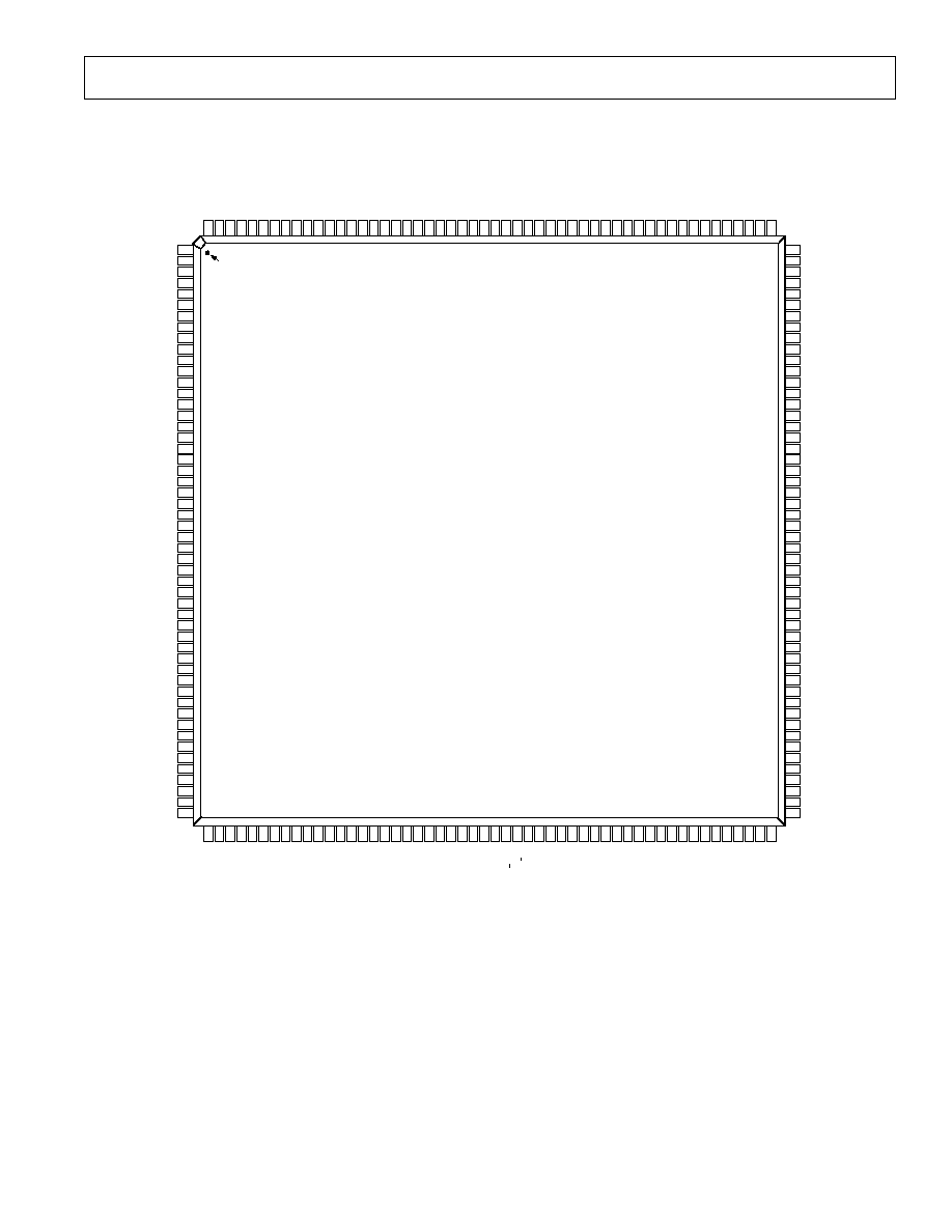
REV. 0
ADSP-2141L
37
PINOUT
PCI Mode
208
207
206
205
204
203
202
201
200
199
198
197
196
195
194
193
192
191
189
188
187
186
185
184
183
182
181
180
190
179
178
177
175
174
173
172
171
170
176
169
168
167
165
164
163
162
161
160
159
158
157
166
71
72
73
74
75
76
77
78
79
80
53
54
55
56
57
58
59
60
61
62
63
64
65
66
67
68
69
70
81
82
83
84
86
87
88
89
90
85
91
92
93
94
96
97
98
99
95
10
0
10
1
102
103
104
5
4
3
2
7
6
9
8
1
14
13
12
11
16
15
17
10
19
18
23
22
21
20
25
24
27
26
29
28
32
31
30
34
33
36
35
40
39
38
37
41
43
42
45
44
50
49
48
47
46
52
51
152
153
154
155
150
151
156
148
149
143
144
145
146
141
142
140
147
138
139
134
135
136
137
132
133
130
131
128
129
125
126
127
123
124
121
122
120
117
118
119
116
114
115
112
113
107
108
109
110
111
105
106
OO
MPLX_BUS/Pci_ad[24]
MPLX1/Pci_
cbe3
MPLX_BUS/Pci_ad[23]
MPLX_BUS/Pci_ad[22]
VDD
GND
MPLX_BUS/Pci_ad[21]
MPLX_BUS/Pci_ad[20]
MPLX_BUS/Pci_ad[20]
MPLX_BUS/Pci_ad[18]
GND
VDD
VDD
GND
MPLX_BUS/Pci_ad[17]
MPLX_BUS/Pci_ad[16]
MPLX2/Pci_
cbe2
PCI_
IRDY
VDD
GND
PCI_
STOP
MPLX10/Pci_P
err
MPLX11/Pci_
serr
PCI_PAR
VDD
GND
MPLX3/Pci_
cbe1
MPLX7/Pci_
f
rame
MPLX9/Pci_
t
rdy
MPLX8/Pci_
devsel
GND
VDD
VDD
GND
MPLX6/Pci_
gnt
MPLX5/Pci_idsel
MPLX_BUS/Pci_ad[15]
MPLX_BUS/Pci_ad[14]
MPLX_BUS/Pci_ad[13]
MPLX_BUS/Pci_ad[12]
VDD
GND
MPLX_BUS/Pci_ad[11]
MPLX_BUS/Pci_ad[10]
MPLX_BUS/Pci_ad[9]
MPLX_BUS/Pci_ad[8]
VDD
GND
MPLX4/Pci_
cbe0
MPLX_BUS/Pci_ad[7]
MPLX_BUS/Pci_ad[6]
MPLX_BUS/Pci_ad[5]
PIN 1
IDENTIFIER
TOP VIEW
(Not to Scale)
ERESET
ADDR[25]
ADDR[24]
ADDR[23]
ADDR[22]
ADDR[21]
ADDR[20]
ADDR[19]
ADDR[18]
ADDR[14]
ADDR[17]
ADDR[16]
ADDR[15]
ADDR[13]
ADDR[12]
ADDR[11]
ADDR[10]
ADDR[6]
ADDR[3]
ADDR[2]
ADDR[1]
CLKIN
VDD
PMS
DMSL
VDD
MPLX_BUS/Pci_ad[1]
GND
VDD
MPLX_BUS/Pci_ad[4]
MPLX_BUS/Pci_ad[3]
MPLX_BUS/Pci_ad[2]
MPLX_BUS/Pci_ad[0]
GND
CLKOUT
RD
WR
GND
DMSH
BMS
CMS
XTAL
GND
ADDR[0]
ADDR[4]
ADDR[5]
ADDR[7]
ADDR[8]
ADDR[9]
VDD
GND
VDD
IOMS
EMS
EE
GND
ECLK
ELOUT
ELIN
EINT
EBR
EBG
MMAP
BMODE
BUS_MODE
BUS_SEL
EE_SK
EE_CS
EE_DI
EE_DO
VDD
GND
PF[7]/
INT_H
PF[6]
PF[5]
PF[4]
PF[3]
PF[2]
PF[1]
PF[0]
PWD
PWDACK
BR
BG
BGH
IRQE
IRQL0
IRQL1
IRQ2
VDD
GND
MPLX_
RESET
/Pci_
rst
MPLX12/Pci_
req
MPLX_BUS/Pci_ad[31]
VDD
PCI_CLK
GND
MPLX_BUS/Pci_ad[30]
MPLX_BUS/Pci_ad[29]
MPLX_BUS/Pci_ad[28]
MPLX_BUS/Pci_ad[27]
VDD
GND
MPLX_BUS/Pci_ad[26]
MPLX_BUS/Pci_ad[25]
GND
VDD
GND
VDD
GND
VDD
GND
VDD
GND
SCLK1
ADSP-2141L
DATA[31]
DATA[30]
DATA[29]
DATA[28]
DATA[27]
DATA[26]
DATA[25]
DATA[24]
DATA[23]
DATA[22]
DATA[21]
DATA[20]
DATA[19]
DATA[18]
DATA[17]
DATA[16]
DATA[15]
DATA[14]
DATA[13]
DATA[12]
DATA[11]
DATA[10]
DATA[9]
DATA[8]
DATA[7]
DATA[6]
DATA[5]
DATA[4]
DATA[3]
DATA[2]
DATA[1]
DATA[0]
RFS
1 TFS1
DT1
SCLK0
DR0
RFS0
TFS0
DT0
PCI MODE
DR1

REV. 0
ADSP-2141L
38
PINOUT
2183-Mode
208
207
206
205
204
203
202
201
200
199
198
197
196
195
194
193
192
191
189
188
187
186
185
184
183
182
181
180
190
179
178
177
175
174
173
172
171
170
176
169
168
167
165
164
163
162
161
160
159
158
157
166
71
72
73
74
75
76
77
78
79
80
53
54
55
56
57
58
59
60
61
62
63
64
65
66
67
68
69
70
81
82
83
84
86
87
88
89
90
85
91
92
93
94
96
97
98
99
95
10
0
10
1
102
103
104
5
4
3
2
7
6
9
8
1
14
13
12
11
16
15
17
10
19
18
23
22
21
20
25
24
27
26
29
28
32
31
30
34
33
36
35
40
39
38
37
41
43
42
45
44
50
49
48
47
46
52
51
152
153
154
155
150
151
156
148
149
143
144
145
146
141
142
140
147
138
139
134
135
136
137
132
133
130
131
128
129
125
126
127
123
124
121
122
120
117
118
119
116
114
115
112
113
107
108
109
110
111
105
106
OO
PIN 1
IDENTIFIER
TOP VIEW
(Not to Scale)
EE
GND
ECLK
ELOUT
ELIN
VDD
GND
PWDACK
VDD
GND
EMS
EINT
EBR
EBG
MMAP
BMODE
BUS_MODE
BUS_SEL
EE_SK
EE_CS
EE_DI
EE_DO
PF[7]/
INT_H
PF[6]
PF[5]
PF[4]
PF[3]
PF[2]
PF[1]
PF[0]
PWD
BR
BG
BGH
IRQE
IRQL0
IRQL1
IRQ2
MPLX_
RESET
/RESET_1
MPLX12/FL2
MPLX_BUS/NC[31]
GND
MPLX_BUS/NC[30]
MPLX_BUS/NC[29]
MPLX_BUS/NC[28]
MPLX_BUS/NC[27]
VDD
GND
MPLX_BUS/NC[26]
MPLX_BUS/NC[25]
PCI_CLK
VDD
ADSP-2141L
ERESET
DATA[31]
DATA[30]
DATA[29]
DATA[28]
DATA[27]
DATA[26]
DATA[25]
DATA[24]
DATA[23]
DATA[22]
GND
VDD
DATA[21]
DATA[20]
DATA[19]
DATA[18]
DATA[17]
DATA[16]
GND
VDD
DATA[15]
DATA[14]
DATA[13]
DATA[12]
DATA[11]
DATA[10]
DATA[9]
DATA[8]
DATA[7]
DATA[6]
DATA[5]
DATA[4]
GND
VDD
DATA[3]
DATA[2]
DATA[1]
DATA[0]
GND
VDD
GND
SCLK1
DR1
RFS1
TFS1
DT1
SCLK0
DR0
RFS0
TFS0
DT0
ADDR[25]
ADDR[24]
ADDR[23]
ADDR[22]
ADDR[21]
ADDR[20]
VDD
ADDR[19]
ADDR[18]
ADDR[14]
ADDR[17]
ADDR[16]
ADDR[15]
GND
ADDR[13]
ADDR[12]
ADDR[11
]
ADDR[10]
ADDR[6]
ADDR[3]
ADDR[2]
ADDR[1]
CLKIN
VDD
PMS
DMSL
VDD
MPLX_BUS/IAD[1
]
GND
VDD
MPLX_BUS/IAD[4]
MPLX_BUS/IAD[3]
MPLX_BUS/IAD[2]
MPLX_BUS/IAD[0]
GND
CLKOUT
WR
GND
DMSH
BMS
CMS
IOMS
XTAL
GND
ADDR[0]
VDD
ADDR[4]
ADDR[5]
ADDR[7]
ADDR[8]
ADDR[9
]
RD
2183 MODE
VDD
GND
GND
VDD
VDD
GND
VDD
GND
VDD
GND
GND
VDD
VDD
GND
MPLX_BUS/NC[24]
MPLX1/NC
MPLX_BUS/NC[23]
MPLX_BUS/NC[22]
MPLX_BUS/NC[21]
MPLX_BUS/NC[20]
MPLX_BUS/NC[19]
MPLX_BUS/NC[18]
MPLX_BUS/NC[17]
MPLX_BUS/NC[16]
MPLX2/NC
PCI_
IRDY
PCI_
STOP
MPLX10/FL0
MPLX11/FL1
PCI_PAR
MPLX3/NC
MPLX7/IS
MPLX9/
IACK
MPLX8/IAL
MPLX6/
IWR
MPLX5/
IRD
MPLX_BUS/IAD[15]
MPLX_BUS/IAD[14]
MPLX_BUS/IAD[13]
MPLX_BUS/IAD[12]
VDD
GND
MPLX_BUS/IAD[11]
MPLX_BUS/IAD[10]
MPLX_BUS/IAD[9]
MPLX_BUS/IAD[8]
VDD
GND
MPLX4/NC
MPLX_BUS/IAD[7]
MPLX_BUS/IAD[6]
MPLX_BUS/IAD[5]
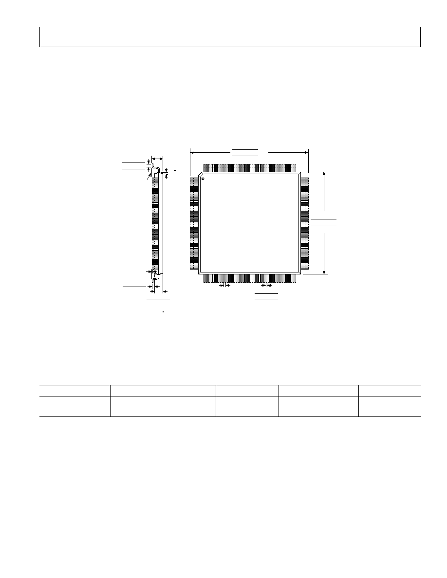
REV. 0
ADSP-2141L
39
PACKAGE DESCRIPTION
Package Details
The package shown below is a 208-lead metric quad flatpack. Measurements are listed in English and (metric). Because this package
is designed as a metric package, Analog Devices recommends that you use these measurements for any PCB layout.
OUTLINE DIMENSIONS
Dimensions shown in inches and (mm).
208-Lead Metric Plastic Quad Flatpack (MQFP)
(Nonhermetic)
1
208
157
156
105
104
53
52
TOP VIEW
(PINS DOWN)
0.020 (0.50)
BSC
1.256 (31.40)
1.248 (31.20) SQ
1.240 (31.00)
1.124 (28.10)
1.120 (28.00) SQ
1.116 (27.90)
0.011 (0.27)
0.009 (0.22)
0.007 (0.17)
LEAD PITCH
LEAD WIDTH
SEATING
PLANE
0.164 (4.10)
MAX
0.003 (0.08)
MAX LEAD
COPLANARITY
0.020 (0.50)
0.010 (0.25)
0.144 (3.59)
0.136 (3.39)
10
TYP
0.041 (1.03)
0.035 (0.88)
0.031 (0.78)
NOTE:
THE ACTUAL POSITION OF EACH LEAD IS WITHIN 0.003 (0.08) FROM ITS IDEAL
POSITION WHEN MEASURED IN THE LATERAL DIRECTION.
CENTER FIGURES ARE TYPICAL UNLESS OTHERWISE NOTED.
THE 208 LEAD MQFP IS A METRIC PACKAGE. ENGLISH DIMENSIONS PROVIDED
ARE APPROXIMATE AND MUST NOT BE USED FOR BOARD DESIGN PURPOSES
ORDERING GUIDE
Part Number
Ambient Temperature Range
Instruction Rate
Package Description
Package Option
ADSP-2141LKS-N1
1
0
°
C to +70
°
C
40 MHz
208-Lead MQFP
S-208
ADSP-2141LKS-E1
2
0
°
C to +70
°
C
40 MHz
208-Lead MQFP
S-208
NOTES
1
The
ADSP-2141LKS-N1 is an electrically equivalent, full function, production (non x-grade) version of the product described in this data sheet. (Full function =
Triple DES enabled, full 168-bit key length, full 2048-bit public key lengths, red keys allowed.)
2
The ADSP-2141LKS-E1 is an electrically equivalent, full function, production (non x-grade) version of the product d escribed in this data sheet except for the following:
Encryption: DES only, with maximum 56-bit key length. Triple DES is disabled.
Public Key Algorithms: Public Key Algorithms limited to 1024-bit max modulus. Red keys not allowed in hardware crypto context.
C365451/00 (rev. 0)
PRINTED IN U.S.A.