Äîêóìåíòàöèÿ è îïèñàíèÿ www.docs.chipfind.ru
a
S
DSP Microcomputer
Information furnished by Analog Devices is believed to be accurate and
reliable. However, no responsibility is assumed by Analog Devices for its
use, nor for any infringements of patents or other rights of third parties that
may result from its use. No license is granted by implication or otherwise
under any patent or patent rights of Analog Devices. Trademarks and
registered trademarks are the property of their respective companies.
REV. A
SHARC and the SHARC logo are registered trademarks of Analog Devices, Inc.
ADSP-21161N
SUMMARY
High Performance 32-Bit DSP--Applications in Audio,
Medical, Military, Wireless Communications,
Graphics, Imaging, Motor-Control, and Telephony
Super Harvard Architecture--Four Independent Buses
for Dual Data Fetch, Instruction Fetch, and
Nonintrusive, Zero-Overhead I/O
Code Compatible with All Other SHARC Family DSPs
Single-Instruction-Multiple-Data (SIMD) Computational
Architecture--Two 32-Bit IEEE Floating-Point
Computation Units, Each with a Multiplier, ALU,
Shifter, and Register File
Serial Ports Offer I
2
S Support Via 8 Programmable and
Simultaneous Receive or Transmit Pins, which
Support up to 16 Transmit or 16 Receive Channels of
Audio
Integrated Peripherals--Integrated I/O Processor,
1M Bit On-Chip Dual-Ported SRAM, SDRAM
Controller, Glueless Multiprocessing Features, and
I/O Ports (Serial, Link, External Bus, SPI, and JTAG)
ADSP-21161N Supports 32-Bit Fixed, 32-Bit Float, and
40-Bit Floating-Point Formats
KEY FEATURES
100 MHz (10 ns) Core Instruction Rate
Single-Cycle Instruction Execution, Including SIMD
Operations in Both Computational Units
600 MFLOPs Peak and 400 MFLOPs Sustained
Performance
225-Ball 17 mm
×
17 mm MBGA Package
FUNCTIONAL BLOCK DIAGRAM
ALU
MULT
DATA
REGISTER
FILE
(PEY)
16
40-BIT
BARREL
SHIFTER
BARREL
SHIFTER
ALU
DATA
REGISTER
FILE
(PEX)
16
40-BIT
TIMER
INSTRUCTION
CACHE
32
48-BIT
DAG1
8
4
32
PROGRAM
SEQUENCER
32
PM ADDRESS BUS
DM ADDRESS BUS
32
BUS
CONNECT
(PX)
PM DATA BUS
DM DATA BUS
64
64
CORE PROCESSOR
SPI PORTS (1)
SERIAL PORTS (4)
LINK PORTS (2)
DMA
CONTROLLER
5
16
20
4
IOP
REGISTERS
(MEMORY MAPPED)
CONTROL,
STATUS, &
DATA BUFFERS
I/O PROCESSOR
TWO INDEPENDENT
DUAL-PORTED BLOCKS
ADDR
DATA
DATA
DATA
ADDR
ADDR
DATA
ADDR
PROCESSOR PORT
I/O PORT
B
L
O
C
K
0
B
L
O
C
K
1
DUAL-PORTED SRAM
HOST PORT
ADDR BUS
MUX
MULTIPROCESSOR
INTERFACE
DATA BUS
MUX
32
24
EXTERNAL PORT
6
12
8
JTAG TEST
AND EMULATION
GPIO
FLAGS
SDRAM
CONTROLLER
IOA
18
IOD
64
DAG2
8
4
32
MULT
One Technology Way, P.O.Box 9106, Norwood, MA 02062-9106, U.S.A.
Tel:781/329-4700
www.analog.com
Fax:781/326-8703
©
2003 Analog Devices, Inc. All rights reserved.

ADSP-21161N
2
REV. A
KEY FEATURES (continued)
1 M Bit On-Chip Dual-Ported SRAM (0.5 M Bit Block 0,
0.5 M Bit Block 1) for Independent Access by Core
Processor and DMA
200 Million Fixed-Point MACs Sustained Performance
Dual Data Address Generators (DAGs) with Modulo and
Bit-Reverse Addressing
Zero-Overhead Looping with Single-Cycle Loop Setup,
Providing Efficient Program Sequencing
IEEE 1149.1 JTAG Standard Test Access Port and On-Chip
Emulation
Single Instruction Multiple Data (SIMD) Architecture
Provides:
Two Computational Processing Elements
Concurrent Execution--Each Processing Element
Executes the Same Instruction, but Operates on
Different Data
Code Compatibility--At Assembly Level, Uses the
Same Instruction Set as Other SHARC DSPs
Parallelism in Buses and Computational Units Enables:
Single-Cycle Execution (with or without SIMD) of: a
Multiply Operation, an ALU Operation, a Dual
Memory Read or Write, and an Instruction Fetch
Transfers Between Memory and Core at Up to Four
32-Bit Floating- or Fixed-Point Words Per Cycle,
Sustained 1.6 Gbytes/s Bandwidth
Accelerated FFT Butterfly Computation through a
Multiply with Add and Subtract
DMA Controller Supports:
14 Zero-Overhead DMA Channels for Transfers between
ADSP-21161N Internal Memory and External Memory,
External Peripherals, Host Processor, Serial Ports,
Link Ports, or Serial Peripheral Interface (SPI-
Compatible)
64-Bit Background DMA Transfers at Core Clock Speed,
in Parallel with Full-Speed Processor Execution
800 M Bytes/s Transfer Rate over IOP Bus
Host Processor Interface to 8-, 16-, and 32-Bit
Microprocessors; the Host Can Directly Read/Write
ADSP-21161N IOP Registers
32-Bit (or up to 48-Bit) Wide Synchronous External Port
Provides:
Glueless Connection to Asynchronous, SBSRAM and
SDRAM External Memories
Memory Interface Supports Programmable Wait State
Generation and Wait Mode for Off-Chip Memory
Up to 50 MHz Operation for Non-SDRAM Accesses
1:2, 1:3, 1:4, 1:6, 1:8 Clock into Core Clock Frequency
Multiply Ratios
24-Bit Address, 32-Bit Data Bus. 16 Additional Data
Lines via Multiplexed Link Port Data Pins Allow
Complete 48-Bit Wide Data Bus for Single-Cycle
External Instruction Execution
Direct Reads and Writes of IOP Registers from Host or
Other 21161N DSPs
62.7 Mega-Word Address Range for Off-Chip SRAM and
SBSRAM Memories
32-48, 16-48, 8-48 Execution Packing for Executing
Instruction Directly from 32-Bit, 16-Bit, or 8-Bit Wide
External Memories
32-48, 16-48, 8-48, 32-32/64, 16-32/64, 8-32/64, Data
Packing for DMA Transfers Directly from 32-Bit,
16-Bit, or 8-Bit Wide External Memories to and from
Internal 32-, 48-, or 64-Bit Internal Memory
Can be Configured to have 48-Bit Wide External Data
Bus, if Link Ports are not Used. The Link Port Data
Lines are Multiplexed with the Data Lines D0 to D15
and are Enabled through Control Bits in SYSCON
SDRAM Controller for Glueless Interface to Low Cost
External Memory
Zero Wait State, 100 MHz Operation for Most Accesses
Extended External Memory Banks (64 M Words) for
SDRAM Accesses
Page Sizes up to 2048 Words
An SDRAM Controller Supports SDRAM in Any and All
Memory Banks
Support for Interface to Run at Core Clock and Half the
Core Clock Frequency
Support for 16 M Bits, 64 M Bits, 128 M Bits, and
256 M Bits with SDRAM Data Bus Configurations of
4, 8, 16, and 32
254 Mega-Word Address Range for Off-Chip SDRAM
Memory
Multiprocessing Support Provides:
Glueless Connection for Scalable DSP Multiprocessing
Architecture
Distributed On-Chip Bus Arbitration for Parallel Bus
Connect of Up to Six ADSP-21161Ns, Global Memory,
and a Host
Two 8-Bit Wide Link Ports for Point-to-Point
Connectivity Between ADSP-21161Ns
400 M Bytes/s Transfer Rate over Parallel Bus
200 M Bytes/s Transfer Rate Over Link Ports
Serial Ports Provide:
Four 50 M Bit/s Synchronous Serial Ports with
Companding Hardware
8 Bidirectional Serial Data Pins, Configurable as Either a
Transmitter or Receiver
I
2
S Support, Programmable Direction for 8
Simultaneous Receive and Transmit Channels, or Up
to Either 16 Transmit Channels or 16 Receive
Channels
128 Channel TDM Support for T1 and E1 Interfaces
Companding Selection on a Per Channel Basis in TDM
Mode
Serial Peripheral Interface (SPI)
Slave Serial Boot through SPI from a Master SPI Device
Full-Duplex Operation
Master-Slave Mode Multimaster Support
Open-Drain Outputs
Programmable Baud Rates, Clock Polarities and Phases
12 Programmable I/O Pins
1 Programmable Timer
3
REV. A
ADSP-21161N
TABLE OF CONTENTS
GENERAL DESCRIPTION . . . . . . . . . . . . . . . . . . . . 3
ADSP-21161N Family Core Architecture . . . . . . . . . 5
SIMD Computational Engine . . . . . . . . . . . . . . . . 5
Independent, Parallel Computation Units . . . . . . . 5
Data Register File . . . . . . . . . . . . . . . . . . . . . . . . . 5
Single-Cycle Fetch of Instruction and
Four Operands . . . . . . . . . . . . . . . . . . . . . . . . . . 5
Instruction Cache . . . . . . . . . . . . . . . . . . . . . . . . . 5
Data Address Generators With Hardware Circular
Buffers . . . . . . . . . . . . . . . . . . . . . . . . . . . . . . . . 5
Flexible Instruction Set . . . . . . . . . . . . . . . . . . . . . 5
ADSP-21161N Memory and I/O Interface Features . 5
Dual-Ported On-Chip Memory . . . . . . . . . . . . . . . 5
Off-Chip Memory and Peripherals Interface . . . . . 6
SDRAM Interface . . . . . . . . . . . . . . . . . . . . . . . . . 6
Target Board JTAG Emulator Connector . . . . . . . 7
DMA Controller . . . . . . . . . . . . . . . . . . . . . . . . . . 7
Multiprocessing . . . . . . . . . . . . . . . . . . . . . . . . . . . 7
Link Ports . . . . . . . . . . . . . . . . . . . . . . . . . . . . . . . 7
Serial Ports . . . . . . . . . . . . . . . . . . . . . . . . . . . . . . 8
Serial Peripheral (Compatible) Interface . . . . . . . . 9
Host Processor Interface . . . . . . . . . . . . . . . . . . . . 9
General-Purpose I/O Ports . . . . . . . . . . . . . . . . . . . 9
Program Booting . . . . . . . . . . . . . . . . . . . . . . . . . . 9
Phase-Locked Loop and Crystal Double Enable . . 9
Power Supplies . . . . . . . . . . . . . . . . . . . . . . . . . . . 9
Development Tools . . . . . . . . . . . . . . . . . . . . . . . . . . 9
Designing an Emulator-Compatible
DSP Board (Target) . . . . . . . . . . . . . . . . . . . . . 10
Additional Information . . . . . . . . . . . . . . . . . . . . . . 11
PIN FUNCTION DESCRIPTIONS . . . . . . . . . . . . . 12
BOOT MODES . . . . . . . . . . . . . . . . . . . . . . . . . . . . . 17
SPECIFICATIONS . . . . . . . . . . . . . . . . . . . . . . . . . . 18
ABSOLUTE MAXIMUM RATINGS . . . . . . . . . . 19
ESD SENSITIVITY . . . . . . . . . . . . . . . . . . . . . . . . 19
TIMING SPECIFICATIONS . . . . . . . . . . . . . . . . 20
Power Dissipation . . . . . . . . . . . . . . . . . . . . . . . . 21
Power-up Sequencing Silicon
Revision 0.3, 1.0, 1.1 . . . . . . . . . . . . . . . . . . . . 22
Clock Input . . . . . . . . . . . . . . . . . . . . . . . . . . . . . 24
Clock Signals . . . . . . . . . . . . . . . . . . . . . . . . . . . . 24
Reset . . . . . . . . . . . . . . . . . . . . . . . . . . . . . . . . . . 25
Interrupts . . . . . . . . . . . . . . . . . . . . . . . . . . . . . . 25
Timer . . . . . . . . . . . . . . . . . . . . . . . . . . . . . . . . . 26
Flags . . . . . . . . . . . . . . . . . . . . . . . . . . . . . . . . . . 26
Memory Read Bus Master . . . . . . . . . . . . . . . . 27
Memory Write Bus Master . . . . . . . . . . . . . . . . 28
Synchronous Read/Write Bus Master . . . . . . . . 29
Synchronous Read/Write Bus Slave . . . . . . . . . . 30
Host Bus Request . . . . . . . . . . . . . . . . . . . . . . . . 31
Asynchronous Read/Write
Host to ADSP-21161N . . . . . . . . . . . . . . . . . . 33
Three-State Timing Bus Master, Bus Slave . . . . 35
DMA Handshake . . . . . . . . . . . . . . . . . . . . . . . . 37
SDRAM Interface Bus Master . . . . . . . . . . . . . 39
Link Ports . . . . . . . . . . . . . . . . . . . . . . . . . . . . . . 41
Serial Ports . . . . . . . . . . . . . . . . . . . . . . . . . . . . . 43
SPI Interface Specifications . . . . . . . . . . . . . . . . . 47
JTAG Test Access Port and Emulation . . . . . . . . 50
Output Drive Currents . . . . . . . . . . . . . . . . . . . . . . 51
Test Conditions . . . . . . . . . . . . . . . . . . . . . . . . . . . 51
Output Enable Time . . . . . . . . . . . . . . . . . . . . . . 51
Output Disable Time . . . . . . . . . . . . . . . . . . . . . 51
Example System Hold Time Calculation . . . . . . . 51
Capacitive Loading . . . . . . . . . . . . . . . . . . . . . . . 52
Environmental Conditions . . . . . . . . . . . . . . . . . . . 52
Thermal Characteristics . . . . . . . . . . . . . . . . . . . 52
225-BALL METRIC MBGA
PIN CONFIGURATIONS . . . . . . . . . . . . . . . . . . 53
OUTLINE DIMENSIONS . . . . . . . . . . . . . . . . . . . . 55
ORDERING GUIDE . . . . . . . . . . . . . . . . . . . . . . . . 55
Revision History . . . . . . . . . . . . . . . . . . . . . . . . . . . . 56
GENERAL DESCRIPTION
The ADSP-21161N SHARC DSP is the first low cost derivative
of the ADSP-21160 featuring Analog Devices Super Harvard
Architecture. Easing portability, the ADSP-21161N is source
code compatible with the ADSP-21160 and with first generation
ADSP-2106x SHARCs in SISD (Single Instruction, Single
Data) mode. Like other SHARC DSPs, the ADSP-21161N is a
32-bit processor that is optimized for high performance DSP
applications. The ADSP-21161N includes a 100 MHz core, a
dual-ported on-chip SRAM, an integrated I/O processor with
multiprocessing support, and multiple internal buses to eliminate
I/O bottlenecks.
As was first offered in the ADSP-21160, the ADSP-21161N
offers a Single-Instruction-Multiple-Data (SIMD) architecture.
Using two computational units (ADSP-2106x SHARCs have
one), the ADSP-21161N can double cycle performance versus
the ADSP-2106x on a range of DSP algorithms.
Fabricated in a state of the art, high speed, low power CMOS
process, the ADSP-21161N has a 10 ns instruction cycle time.
With its SIMD computational hardware running at 100 MHz,
the ADSP-21161N can perform 600 million math operations per
second.
Table 1
shows performance benchmarks for the
ADSP-21161N.
Table 1. Benchmarks (at 100 MHz)
Benchmark Algorithm
Speed
(at 100 MHz)
1024 Point Complex FFT
(Radix 4, with reversal)
171 µs
FIR Filter (per tap)
1
5 ns
IIR Filter (per biquad)
1
40 ns
1
1
Specified in SISD mode. Using SIMD, the same benchmark applies for
two sets of computations. For example, two sets of biquad operations can
be performed in the same amount of time as the SISD mode benchmark.
Matrix Multiply (pipelined)
[3
×
3]
×
[3
×
1]
30 ns
[4
×
4]
×
[4
×
1]
37 ns
Divide (y/x)
60 ns
1
Inverse Square Root
40 ns
1
DMA Transfers
800 M bytes/s
ADSP-21161N
4
REV. A
The ADSP-21161N continues SHARC's industry-leading
standards of integration for DSPs, combining a high performance
32-bit DSP core with integrated, on-chip system features. These
features include a 1 M bit dual ported SRAM memory, host
processor interface, I/O processor that supports 14 DMA
channels, four serial ports, two link ports, SDRAM controller,
SPI interface, external parallel bus, and glueless multiprocessing.
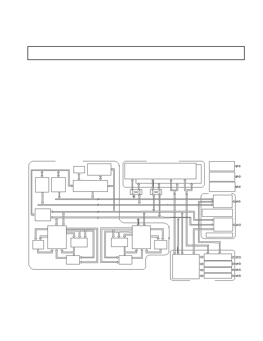
The block diagram of the ADSP-21161N
on Page 1
illustrates
the following architectural features:
·
Two processing elements, each made up of an ALU, Mul-
tiplier, Shifter, and Data Register File
·
Data Address Generators (DAG1, DAG2)
·
Program sequencer with instruction cache
·
PM and DM buses capable of supporting four 32-bit data
transfers between memory and the core every core
processor cycle
·
Interval timer
·
On-Chip SRAM (1 M bit)
·
SDRAM Controller for glueless interface to SDRAMs
·
External port that supports:
·
Interfacing to off-chip memory peripherals
·
Glueless multiprocessing support for six ADSP-
21161N SHARCs
·
Host port read/write of IOP registers
·
DMA controller
·
Four serial ports
·
Two link ports
·
SPI compatible interface
·
JTAG test access port
·
12 General-Purpose I/O Pins
Figure 1
shows a typical single-processor system. A multiprocess-
ing system appears in
Figure 4 on Page 8
.
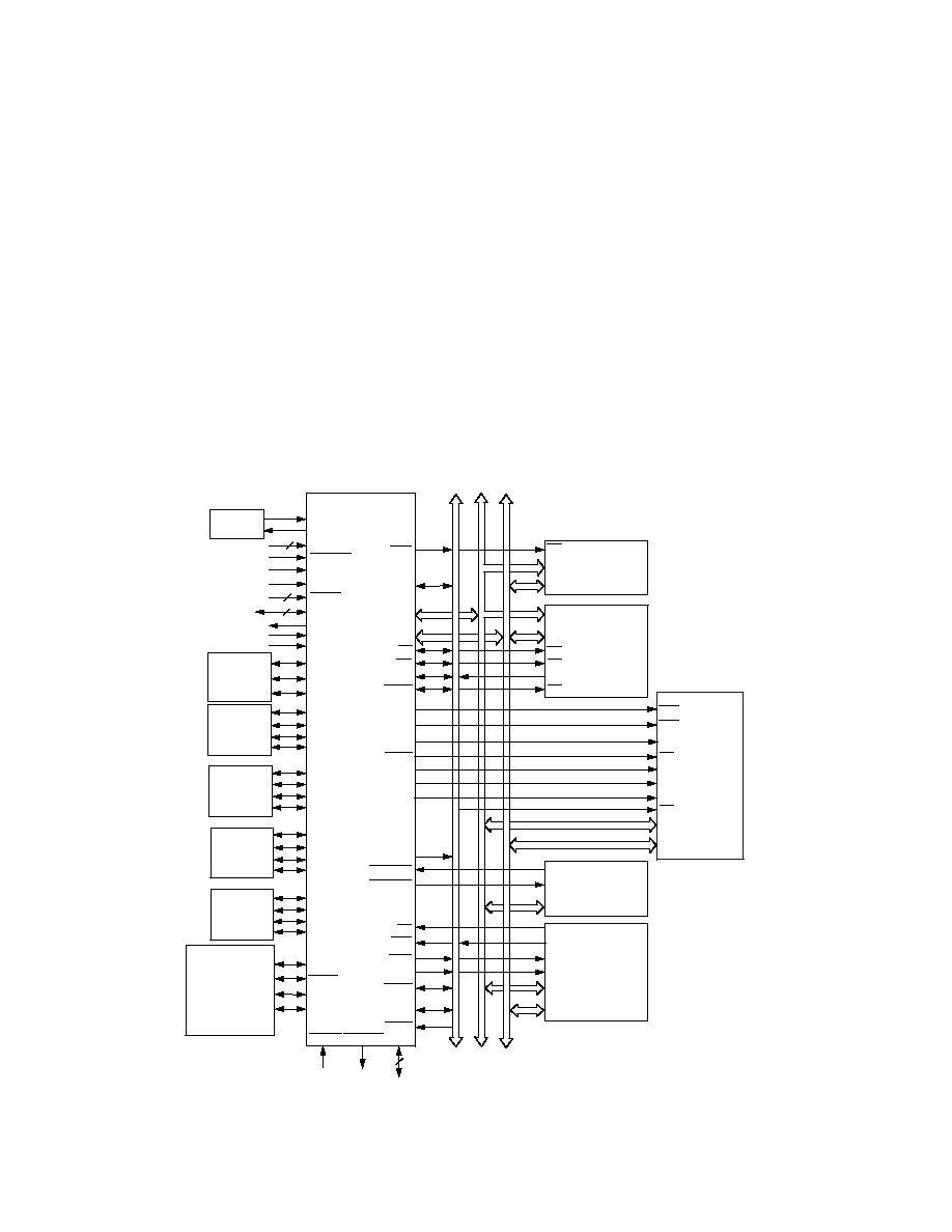
Figure 1. System Diagram
DMA DEVICE
(OPTIONAL)
DATA
CLKOUT
DMAR2-1
DMAG2-1
ADDR
DATA
HOST
PROCESSOR
INTERFACE
(OPTIONAL)
3
12
CLOCK
CLKIN
XTAL
IRQ2-0
2
CLK_CFG1-0
EBOOT
LBOOT
FLAG11-0
TIMEXP
CLKDBL
RESET
JTAG
7
SBTS
ADSP-21161N
BMS
LINK
DEVICES
(2 MAX)
(OPTIONAL)
LXCLK
LXACK
LXDAT7-0
SCLK0
D0B
D0A
FS0
SERIAL
DEVICE
(OPTIONAL)
CS
BOOT
EPROM
(OPTIONAL)
ADDR
MEMORY
AND
PERIPHERALS
(OPTIONAL)
OE
DATA
CS
RD
RAS
ACK
BR6-1
RPBA
ID2-0
PA
HBG
HBR
SDWE
MS3-0
WR
DATA47-16
DATA
ADDR
CS
ACK
WE
ADDR23-0
D
A
T
A
C
O
N
T
R
O
L
A
D
D
R
E
S
S
BRST
SDRAM
(OPTIONAL)
SCLK1
D1B
D1A
FS1
SERIAL
DEVICE
(OPTIONAL)
SCLK2
D2B
D2A
FS2
SERIAL
DEVICE
(OPTIONAL)
SCLK3
D3B
D3A
FS3
SERIAL
DEVICE
(OPTIONAL)
SPICLK
MISO
MOSI
SPIDS
SPI
COMPATIBLE
DEVICE
(HOST OR SLAVE)
(OPTIONAL)
DATA
CAS
RAS
DQM
WE
ADDR
CS
A10
CKE
CLK
DQM
CAS
REDY
SDCKE
SDA10
SDCLK1-0
RSTOUT

5
REV. A
ADSP-21161N
ADSP-21161N Family Core Architecture
The ADSP-21161N includes the following architectural features
of the ADSP-2116x family core. The ADSP-21161N is code
compatible at the assembly level with the ADSP-21160, ADSP-
21060, ADSP-21061, ADSP-21062, and ADSP-21065L.
SIMD Computational Engine
The ADSP-21161N contains two computational processing
elements that operate as a Single Instruction Multiple Data
(SIMD) engine. The processing elements are referred to as PEX
and PEY, and each contains an ALU, multiplier, shifter, and
register file. PEX is always active, and PEY may be enabled by
setting the PEYEN mode bit in the MODE1 register. When this
mode is enabled, the same instruction is executed in both pro-
cessing elements, but each processing element operates on
different data. This architecture is efficient at executing math
intensive DSP algorithms.
Entering SIMD mode also has an effect on the way data is trans-
ferred between memory and the processing elements. When in
SIMD mode, twice the data bandwidth is required to sustain
computational operation in the processing elements. Because of
this requirement, entering SIMD mode also doubles the
bandwidth between memory and the processing elements. When
using the DAGs to transfer data in SIMD mode, two data values
are transferred with each access of memory or the register file.
SIMD is supported only for internal memory accesses and is not
supported for off-chip accesses.
Independent, Parallel Computation Units
Within each processing element is a set of computational units.
The computational units consist of an arithmetic/logic unit
(ALU), multiplier, and shifter. These units perform single-cycle
instructions. The three units within each processing element are
arranged in parallel, maximizing computational throughput.
Single multifunction instructions execute parallel ALU and mul-
tiplier operations. In SIMD mode, the parallel ALU and
multiplier operations occur in both processing elements. These
computation units support IEEE 32-bit single-precision floating-
point, 40-bit extended precision floating-point, and 32-bit
fixed-point data formats.
Data Register File
A general-purpose data register file is contained in each process-
ing element. The register files transfer data between the
computation units and the data buses, and store intermediate
results. These 10-port, 32-register (16 primary, 16 secondary)
register files, combined with the ADSP-2116x enhanced Harvard
architecture, allow unconstrained data flow between computa-
tion units and internal memory. The registers in PEX are referred
to as R0
R15 and in PEY as S0
S15.
Single-Cycle Fetch of Instruction and Four Operands
The ADSP-21161N features an enhanced Harvard architecture
in which the data memory (DM) bus transfers data and the
program memory (PM) bus transfers both instructions and data
(see
Figure 1 on Page 4
). With the ADSP-21161N's separate
program and data memory buses and on-chip instruction cache,
the processor can simultaneously fetch four operands (two over
each data bus) and an instruction (from the cache), all in a
single cycle.
Instruction Cache
The ADSP-21161N includes an on-chip instruction cache that
enables three-bus operation for fetching an instruction and four
data values. The cache is selective--only the instructions whose
fetches conflict with PM bus data accesses are cached. This cache
enables full-speed execution of core, looped operations such as
digital filter multiply-accumulates, and FFT butterfly processing.
Data Address Generators With Hardware Circular
Buffers
The ADSP-21161N's two data address generators (DAGs) are
used for indirect addressing and implementing circular data
buffers in hardware. Circular buffers allow efficient programming
of delay lines and other data structures required in digital signal
processing, and are commonly used in digital filters and Fourier
transforms. The two DAGs of the ADSP-21161N contain suffi-
cient registers to allow the creation of up to 32 circular buffers
(16 primary register sets, 16 secondary). The DAGs automati-
cally handle address pointer wrap-around, reduce overhead,
increase performance, and simplify implementation. Circular
buffers can start and end at any memory location.
Flexible Instruction Set
The 48-bit instruction word accommodates a variety of parallel
operations, for concise programming. For example, the ADSP-
21161N can conditionally execute a multiply, an add, and a
subtract in both processing elements, while branching, all in a
single instruction.
ADSP-21161N Memory and I/O Interface Features
The ADSP-21161N adds the following architectural features to
the ADSP-2116x family core:
Dual-Ported On-Chip Memory
The ADSP-21161N contains one megabit of on-chip SRAM,
organized as two blocks of 0.5 M bits. Each block can be config-
ured for different combinations of code and data storage. Each
memory block is dual-ported for single-cycle, independent
accesses by the core processor and I/O processor. The dual-
ported memory in combination with three separate on-chip buses
allow two data transfers from the core and one from the I/O
processor, in a single cycle. On the ADSP-21161N, the memory
can be configured as a maximum of 32K words of 32-bit data,
64K words of 16-bit data, 21K words of 48-bit instructions (or
40-bit data), or combinations of different word sizes up to one
megabit. All of the memory can be accessed as 16-bit, 32-bit,
48-bit, or 64-bit words. A 16-bit floating-point storage format is
supported that effectively doubles the amount of data that may
be stored on-chip. Conversion between the 32-bit floating-point
and 16-bit floating-point formats is done in a single instruction.
While each memory block can store combinations of code and
data, accesses are most efficient when one block stores data using
the DM bus for transfers, and the other block stores instructions
and data using the PM bus for transfers. Using the DM bus and
ADSP-21161N
6
REV. A
PM bus, with one dedicated to each memory block, assures
single-cycle execution with two data transfers. In this case, the
instruction must be available in the cache.
Off-Chip Memory and Peripherals Interface
The ADSP-21161N's external port provides the processor's
interface to off-chip memory and peripherals. The 62.7-M word
off-chip address space (254.7-M word if all SDRAM) is included
in the ADSP-21161N's unified address space. The separate on-
chip buses--for PM addresses, PM data, DM addresses, DM
data, I/O addresses, and I/O data--are multiplexed at the external
port to create an external system bus with a single 24-bit address
bus and a single 32-bit data bus. Every access to external memory
is based on an address that fetches a 32-bit word. When fetching
an instruction from external memory, two 32-bit data locations
are being accessed for packed instructions. Unused link port lines
can also be used as additional data lines DATA15
DATA0,
allowing single-cycle execution of instructions from external
memory, at up to 100 MHz.
Figure 3 on Page 7
shows the
alignment of various accesses to external memory.
The external port supports asynchronous, synchronous, and syn-
chronous burst accesses. Synchronous burst SRAM can be
interfaced gluelessly. The ADSP-21161N also can interface glue-
lessly to SDRAM. Addressing of external memory devices is
facilitated by on-chip decoding of high-order address lines to
generate memory bank select signals. The ADSP-21161N
provides programmable memory wait states and external
memory acknowledge controls to allow interfacing to memory
and peripherals with variable access, hold, and disable time
requirements.
SDRAM Interface
The SDRAM interface enables the ADSP-21161N to transfer
data to and from synchronous DRAM (SDRAM) at the core
clock frequency or at one-half the core clock frequency. The
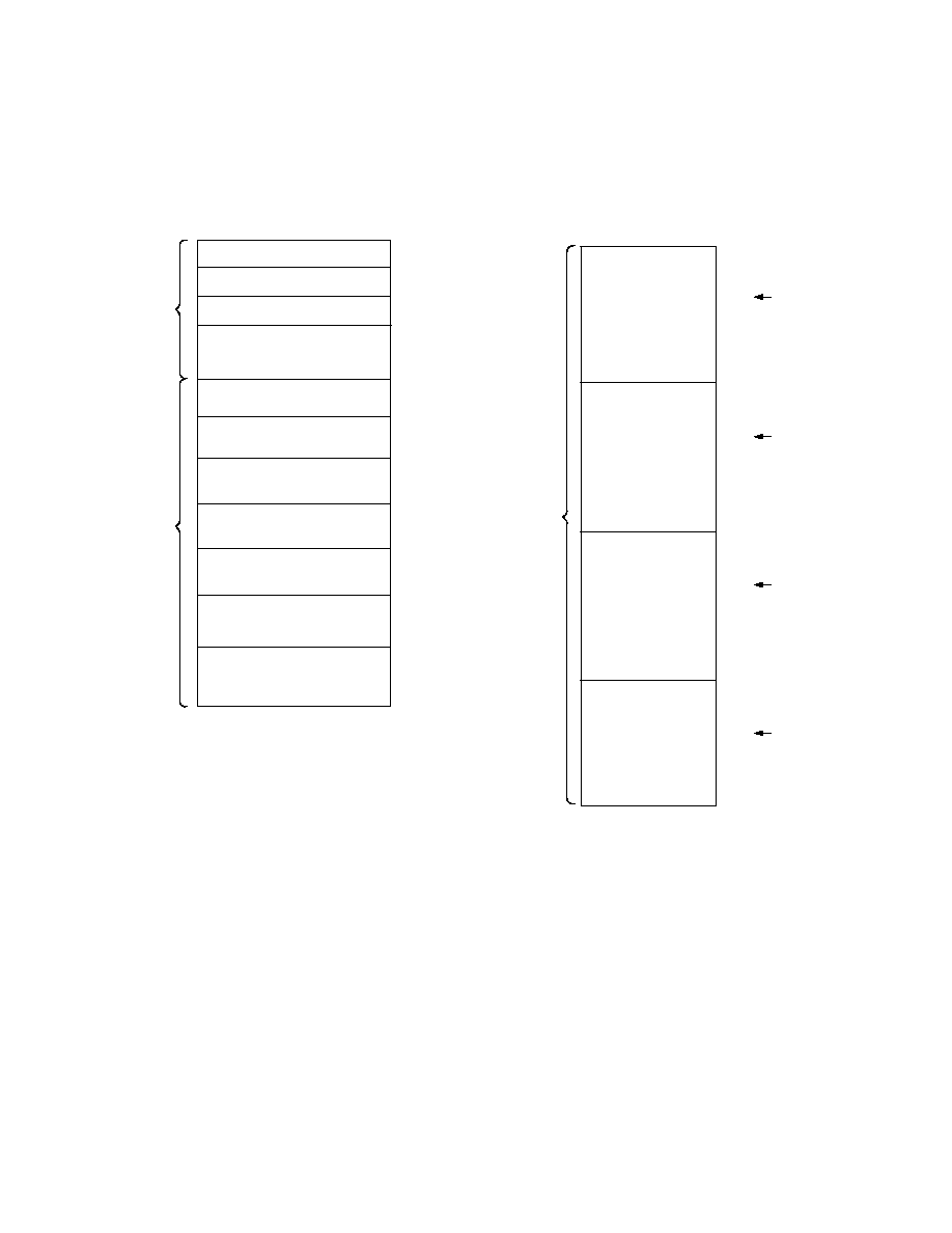
Figure 2. Memory Map
0x000A 0000 - 0x000A 7FFF (BLK 1)
0x0002 8000 - 0x0002 9FFF (BLK 1)
0x0005 0000 - 0x0005 3FFF (BLK 1)
0x0010 0000 - 0x0011 FFFF
0x0004 0000 - 0x0004 3FFF (BLK 0)
0x0008 0000 - 0x0008 7FFF (BLK 0)
0x0012 0000 - 0x0013 FFFF
0x0014 0000 - 0x0015 FFFF
0x0016 0000 - 0x0017 FFFF
0x001A 0000 - 0x001B FFFF
0x0000 0000 - 0x0001 FFFF
0x0002 0000 - 0x0002 1FFF (BLK 0)
0x0020 0000
BANK 1
MS0
BANK 2
MS1
BANK 3
MS2
MS3
IOP REGISTERS
LONG WORD ADDRESSING
SHORT WORD ADDRESSING
NORMAL WORD ADDRESSING
ADDRESS
BANK 0
0x03FF FFFF (SDRAM)
0x00FF FFFF (NON-SDRAM)
0x0400 0000
0x07FF FFFF (SDRAM)
0x04FF FFFF (NON-SDRAM)
0x0800 0000
0x0BFF FFFF (SDRAM)
0x08FF FFFF (NON-SDRAM)
0x0C00 0000
0x0FFF FFFF (SDRAM)
0x0CFF FFFF (NON-SDRAM)
NOTE: BANK SIZES ARE FIXED
0x0018 0000 - 0x0019 FFFF
INTERNAL
MEMORY
SPACE
MULTIPROCESSOR
MEMORY
SPACE
ADDRESS
IOP REGISTERS OF ADSP-21161N
WITH ID = 001
IOP REGISTERS OF ADSP-21161N
WITH ID = 010
IOP REGISTERS OF ADSP-21161N
WITH ID = 011
IOP REGISTERS OF ADSP-21161N
WITH ID = 100
IOP REGISTERS OF ADSP-21161N
WITH ID = 101
IOP REGISTERS OF ADSP-21161N
WITH ID = 110
RESERVED
0
x
001C 0000
0
x
001F FFFF
EXTERNAL MEMORY SPACE
7
REV. A
ADSP-21161N
synchronous approach, coupled with the core clock frequency,
supports data transfer at a high throughput--up to 400 M bytes/s
for 32-bit transfers and 600 M bytes/s for 48-bit transfers.
The SDRAM interface provides a glueless interface with
standard SDRAMs--16 Mb, 64 Mb, 128 Mb, and 256 Mb--
and includes options to support additional buffers between the
ADSP-21161N and SDRAM. The SDRAM interface is
extremely flexible and provides capability for connecting
SDRAMs to any one of the ADSP-21161N's four external
memory banks, with up to all four banks mapped to SDRAM.
Systems with several SDRAM devices connected in parallel may
require buffering to meet overall system timing requirements.
The ADSP-21161N supports pipelining of the address and
control signals to enable such buffering between itself and
multiple SDRAM devices.
Target Board JTAG Emulator Connector
Analog Devices DSP Tools product line of JTAG emulators uses
the IEEE 1149.1 JTAG test access port of the ADSP-21161N
processor to monitor and control the target board processor
during emulation. Analog Devices DSP Tools product line of
JTAG emulators provides emulation at full processor speed,
allowing inspection and modification of memory, registers, and
processor stacks. The processor's JTAG interface ensures that the
emulator will not affect target system loading or timing.
For complete information on SHARC Analog Devices DSP
Tools product line of JTAG emulator operation, see the appro-
priate Emulator Hardware User's Guide. For detailed infor-
mation on the interfacing of Analog Devices JTAG emulators
with Analog Devices DSP products with JTAG emulation ports,
please refer to Engineer to Engineer Note EE-68: Analog Devices
JTAG Emulation Technical Reference. Both of these documents can
be found on the Analog Devices website:
http://www.analog.com/dsp/tech_docs.html
DMA Controller
The ADSP-21161N's on-chip DMA controller enables zero-
overhead data transfers without processor intervention. The
DMA controller operates independently and invisibly to the
processor core, allowing DMA operations to occur while the core
is simultaneously executing its program instructions. DMA
transfers can occur between the ADSP-21161N's internal
memory and external memory, external peripherals, or a host
processor. DMA transfers can also occur between the ADSP-
21161N's internal memory and its serial ports, link ports, or the
SPI-compatible (Serial Peripheral Interface) port. External bus
packing and unpacking of 32-, 48-, or 64-bit words in internal
memory is performed during DMA transfers from either 8-,
16-, or 32-bit wide external memory. Fourteen channels of DMA
are available on the ADSP-21161N--two are shared between the
SPI interface and the link ports, eight via the serial ports, and
four via the processor's external port (for host processor, other
ADSP-21161Ns, memory, or I/O transfers). Programs can be
downloaded to the ADSP-21161N using DMA transfers. Asyn-
chronous off-chip peripherals can control two DMA channels
using DMA Request/Grant lines (
DMAR21, DMAG21).
Other DMA features include interrupt generation upon comple-
tion of DMA transfers, and DMA chaining for automatic linked
DMA transfers.
Multiprocessing
The ADSP-21161N offers powerful features tailored to
multiprocessing DSP systems. The external port and link ports
provide integrated glueless multiprocessing support.
The external port supports a unified address space (see
Figure 2
on Page 6
) that enables direct interprocessor accesses of each
ADSP-21161N's internal memory-mapped (I/O processor) reg-
isters. All other internal memory can be indirectly accessed via
DMA transfers initiated via the programming of the IOP DMA
parameter and control registers. Distributed bus arbitration logic
is included on-chip for simple, glueless connection of systems
containing up to six ADSP-21161Ns and a host processor.
Master processor change over incurs only one cycle of overhead.
Bus arbitration is selectable as either fixed or rotating priority.
Bus lock enables indivisible read-modify-write sequences for
semaphores. A vector interrupt is provided for interprocessor
commands. Maximum throughput for interprocessor data
transfer is 400 M bytes/s over the external port.
Two link ports provide a second method of multiprocessing com-
munications. Each link port can support communications to
another ADSP-21161N. The ADSP-21161N, running at
100 MHz, has a maximum throughput for interprocessor com-
munications over the links of 200 M bytes/s. The link ports and
cluster multiprocessing can be used concurrently or
independently.
Link Ports
The ADSP-21161N features two 8-bit link ports that provide
additional I/O capabilities. With the capability of running at
100 MHz, each link port can support 100 M bytes/s. Link port
I/O is especially useful for point-to-point interprocessor commu-
nication in multiprocessing systems. The link ports can operate
independently and simultaneously, with a maximum data
throughput of 200 M bytes/s. Link port data is packed into
48- or 32-bit words and can be directly read by the core processor
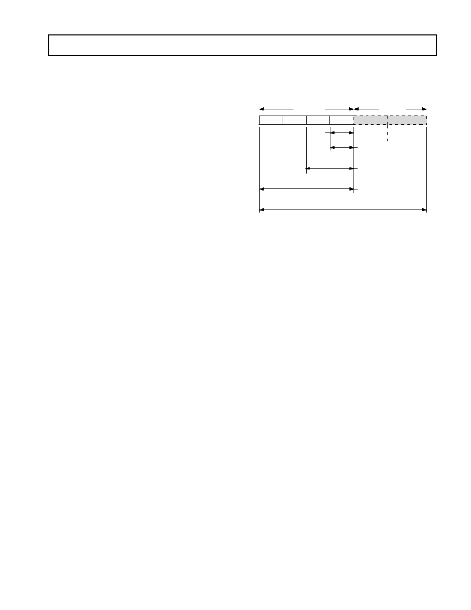
Figure 3. External Data Alignment Options
DATA150
15
8 7
0
L1DATA70
DAT A15-8
L0DATA70
DA TA70
16-BIT PACKED DMA DATA
16-BIT PACKED INSTRUC-
TION EXECUTION
F LOAT OR FIXED, D31D0,
32-BIT PA CKED
32-BIT PA CKED INSTRUC-
T ION
EXTRA DA TA LINES DATA150 AR E ONLY ACCESSIBLE IF LINK PORT S
ARE DISABLED. ENAB LE THESE ADDITIONAL DATA L INKS BY SELECT-
ING IPACK10 = 01 IN SYSCON.
48-BIT INSTRUCT ION FETCH
(NO PACKING)
47
40 39
32 31
24 23
16
DATA4716
8-BIT PACKED DMA D ATA
8-BIT PACKED INST RUCT ION
EXECUTION
PROM
BOOT
NOTE:
ADSP-21161N
8
REV. A
or DMA-transferred to on-chip memory. Each link port has its
own double-buffered input and output registers. Clock/acknowl-
edge handshaking controls link port transfers. Transfers are
programmable as either transmit or receive.
Serial Ports
The ADSP-21161N features four synchronous serial ports that
provide an inexpensive interface to a wide variety of digital and
mixed-signal peripheral devices. Each serial port is made up of
two data lines, a clock and frame sync. The data lines can be
programmed to either transmit or receive.
Figure 4. Shared Memory Multiprocessing System
ACK
OE
ADDR
DATA
CS
WE
GLOBAL
MEMORY
AND
PERIPHERALS
(OPTIONAL)
C
O
N
T
R
O
L
ADSP-21161N #1
ADDR23-0
CONTROL
ADSP-21161N #3
ID2-0
RESET
CLKIN
3
ADSP-21161N #4
CLOCK
ADDR
DATA
SDRAM
(OPTIONAL)
CS
ADDR
DATA
BOOT
EPROM
(OPTIONAL)
ID2-0
RESET
CLKIN
C
O
N
T
R
O
L
A
D
D
R
E
S
S
D
A
T
A
C
O
N
T
R
O
L
A
D
D
R
E
S
S
D
A
T
A
CONTROL
ADSP-21161N #2
ID2-0
RESET
CLKIN
2
1
ADDR
DATA
HOST
PROCESSOR
INTERFACE
(OPTIONAL)
WE
RAS
CAS
DQM
CLK
A10
CKE
CS
DATA47-16
SDWE
RAS
CAS
DQM
SDCLK1-0
SDA10
SDCKE
BR6-2
RD
MS3-0
SBTS
CS
ACK
BR1
REDY
HBG
HBR
WR
BMS
ADDR23-0
RESET
DATA47-16
ADDR23-0
DATA47-16
9
REV. A
ADSP-21161N
The serial ports operate at up to half the clock rate of the core,
providing each with a maximum data rate of 50 M bit/s. The serial
data pins are programmable as either a transmitter or receiver,
providing greater flexibility for serial communications. Serial port
data can be automatically transferred to and from on-chip
memory via a dedicated DMA. Each of the serial ports features
a Time Division Multiplex (TDM) multichannel mode, where
two serial ports are TDM transmitters and two serial ports are
TDM receivers (SPORT0 Rx paired with SPORT2 Tx,
SPORT1 Rx paired with SPORT3 Tx). Each of the serial ports
also support the I
2
S protocol (an industry standard interface
commonly used by audio codecs, ADCs and DACs), with two
data pins, allowing four I
2
S channels (using two I
2
S stereo
devices) per serial port, with a maximum of up to 16 I
2
S channels.
The serial ports permit little-endian or big-endian transmission
formats and word lengths selectable from 3 bits to 32 bits. For
I
2
S mode, data-word lengths are selectable between 8 bits and 32
bits. Serial ports offer selectable synchronization and transmit
modes as well as optional µ-law or A-law companding. Serial port
clocks and frame syncs can be internally or externally generated.
Serial Peripheral (Compatible) Interface
Serial Peripheral Interface (SPI) is an industry standard synchro-
nous serial link, enabling the ADSP-21161N SPI-compatible
port to communicate with other SPI-compatible devices. SPI is
a 4-wire interface consisting of two data pins, one device select
pin, and one clock pin. It is a full-duplex synchronous serial
interface, supporting both master and slave modes. The SPI port
can operate in a multimaster environment by interfacing with up
to four other SPI-compatible devices, either acting as a master or
slave device. The ADSP-21161N SPI-compatible peripheral
implementation also features programmable baud rate and clock
phase/polarities. The ADSP-21161N SPI-compatible port uses
open drain drivers to support a multimaster configuration and to
avoid data contention.
Host Processor Interface
The ADSP-21161N host interface enables easy connection to
standard 8-bit, 16-bit, or 32-bit microprocessor buses with little
additional hardware required. The host interface is accessed
through the ADSP-21161N's external port. Four channels of
DMA are available for the host interface; code and data transfers
are accomplished with low software overhead. The host processor
requests the ADSP-21161N's external bus with the host bus
request (
HBR), host bus grant (HBG), and chip select (CS)
signals. The host can directly read and write the internal IOP
registers of the ADSP-21161N, and can access the DMA channel
setup and message registers. DMA setup via a host would allow
it to access any internal memory address via DMA transfers.
Vector interrupt support provides efficient execution of host
commands.
General-Purpose I/O Ports
The ADSP-21161N also contains 12 programmable, general
purpose I/O pins that can function as either input or output. As
output, these pins can signal peripheral devices; as input, these
pins can provide the test for conditional branching.
Program Booting
The internal memory of the ADSP-21161N can be booted at
system power-up from either an 8-bit EPROM, a host processor,
the SPI interface, or through one of the link ports. Selection of
the boot source is controlled by the Boot Memory Select (
BMS),
EBOOT (EPROM Boot), and Link/Host Boot (LBOOT) pins.
8-, 16-, or 32-bit host processors can also be used for booting.
Phase-Locked Loop and Crystal Double Enable
The ADSP-21161N uses an on-chip Phase-Locked Loop (PLL)
to generate the internal clock for the core. The CLK_CFG1
0
pins are used to select ratios of 2:1, 3:1, and 4:1. In addition to
the PLL ratios, the
CLKDBL pin can be used for more clock
ratio options. The (1
×
/2
×
CLKIN) rate set by the
CLKDBL
pin determines the rate of the PLL input clock and the rate at
which the external port operates. With the combination of
CLK_CFG1
0 and
CLKDBL, ratios of 2:1, 3:1, 4:1, 6:1, and
8:1 between the core and CLKIN are supported. See also
Figure 10 on Page 20
.
Power Supplies
The ADSP-21161N has separate power supply connections for
the analog (AV
DD
/AGND), internal (V
DDINT
), and external
(V
DDEXT
) power supplies. The internal and analog supplies must
meet the 1.8 V requirement. The external supply must meet the
3.3 V requirement. All external supply pins must be connected
to the same supply.
Note that the analog supply (AV
DD
) powers the ADSP-21161N's
clock generator PLL. To produce a stable clock, provide an
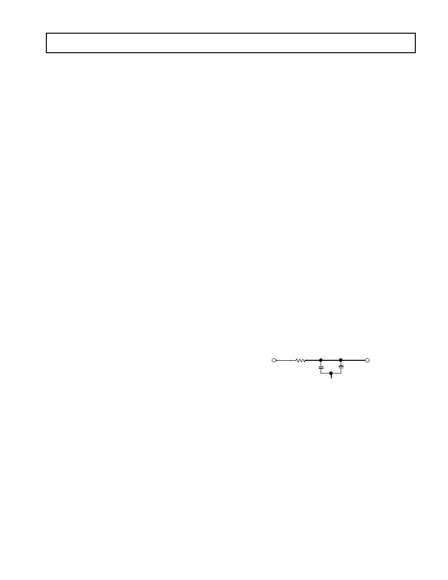
external circuit to filter the power input to the AV
DD
pin. Place
the filter as close as possible to the pin. For an example circuit,
see
Figure 5
. To prevent noise coupling, use a wide trace for the
analog ground (AGND) signal and install a decoupling capacitor
as close as possible to the pin.
Development Tools
The ADSP-21161N is supported with a complete set of software
and hardware development tools, including Analog Devices
emulators and VisualDSP++
1
development environment. The
same emulator hardware that supports other ADSP-21xxx DSPs,
also fully emulates the ADSP-21161N.
The VisualDSP++ project management environment lets pro-
grammers develop and debug an application. This environment
includes an easy-to-use assembler that is based on an algebraic
syntax; an archiver (librarian/library builder), a linker, a loader,
Figure 5. Analog Power (AV
DD
) Filter Circuit
1
VisualDSP++ is a registered trademark of Analog Devices, Inc.
10
V
DDINT
0.1 F
0.01 F
AGND
AV
DD
ADSP-21161N
10
REV. A
a cycle-accurate instruction-level simulator, a C/C++ compiler,
and a C/C++ run-time library that includes DSP and mathemat-
ical functions. Two key points for these tools are:
·
Compiled ADSP-21161N C/C++ code efficiency--The
compiler has been developed for efficient translation of
C/C++ code to ADSP-21161N assembly. The DSP has
architectural features that improve the efficiency of
compiled C/C++ code.
·
ADSP-2106x family code compatibility--The assembler
has legacy features to ease the conversion of existing
ADSP-2106x applications to the ADSP-21161N.
Debugging both C/C++ and assembly programs with the
VisualDSP++ debugger, programmers can:
·
View mixed C/C++ and assembly code (interleaved
source and object information)
·
Insert break points
·
Set conditional breakpoints on registers, memory, and
stacks
·
Trace instruction execution
·
Perform linear or statistical profiling of program
execution
·
Fill, dump, and graphically plot the contents of memory
·
Source level debugging
·
Create custom debugger windows
The VisualDSP++ IDE lets programmers define and manage
DSP software development. Its dialog boxes and property pages
let programmers configure and manage all of the ADSP-21xxx
development tools, including the syntax highlighting in the
VisualDSP++ editor. This capability permits:
·
Controlling how the development tools process inputs
and generate outputs.
·
Maintaining a one-to-one correspondence with the tool's
command line switches.
Analog Devices DSP emulators use the IEEE 1149.1 JTAG test
access port of the ADSP-21161N processor to monitor and
control the target board processor during emulation. The
emulator provides full-speed emulation, allowing inspection and
modification of memory, registers, and processor stacks. Nonin-
trusive in-circuit emulation is assured by the use of the processor's
JTAG interface--the emulator does not affect target system
loading or timing.
In addition to the software and hardware development tools
available from Analog Devices, third parties provide a wide range
of tools supporting the ADSP-21xxx processor family. Hardware
tools include ADSP-21xxx PC plug-in cards. Third Party
software tools include DSP libraries, real-time operating systems,
and block diagram design tools.
Designing an Emulator-Compatible DSP Board
(Target)
The Analog Devices DSP Tools family of emulators are tools that
every DSP developer needs to test and debug hardware and
software systems. Analog Devices has supplied an IEEE 1149.1
JTAG Test Access Port (TAP) on each JTAG DSP. The emulator
uses the TAP to access the internal features of the DSP, allowing
the developer to load code, set breakpoints, observe variables,
observe memory, and examine registers. The DSP must be halted
to send data and commands, but once an operation has been
completed by the emulator, the DSP system is set running at full
speed with no impact on system timing.
To use these emulators, the target's design must include the
interface between an Analog Devices JTAG DSP and the
emulation header on a custom DSP target board.
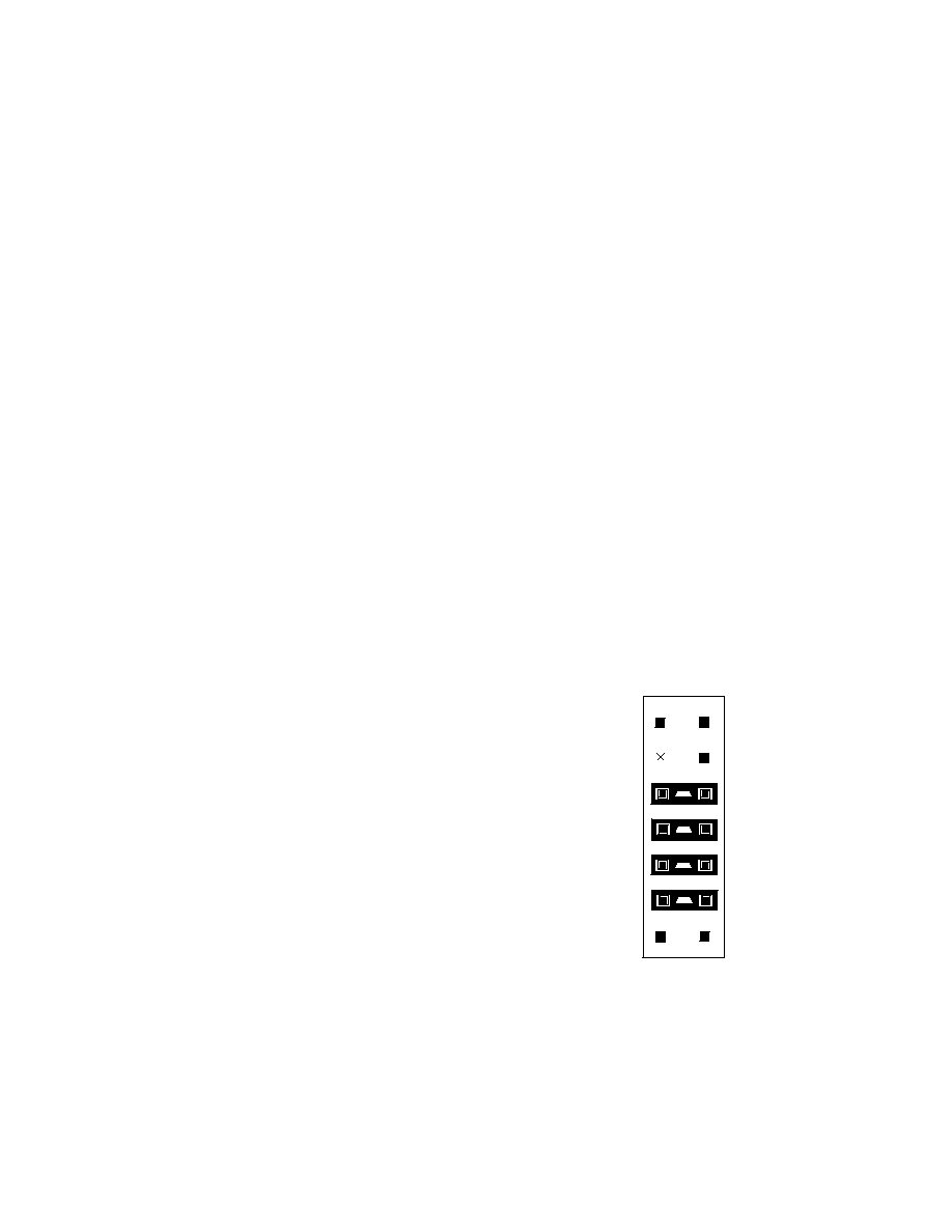
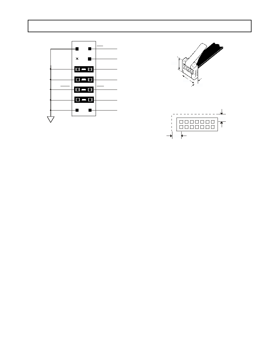
Target Board Header
The emulator interface to an Analog Devices JTAG DSP is a
14-pin header, as shown in
Figure 6
. The customer must supply
this header on the target board in order to communicate with the
emulator. The interface consists of a standard dual row 0.025"
square post header, set on 0.1"
×
0.1" spacing, with a minimum
post length of 0.235". Pin 3 is the key position used to prevent
the pod from being inserted backwards. This pin must be clipped
on the target board.
Also, the clearance (length, width, and height) around the header
must be considered. Leave a clearance of at least 0.15" and 0.10"
around the length and width of the header, and reserve a height
clearance to attach and detach the pod connector.
As can be seen in
Figure 6
, there are two sets of signals on the
header. There are the standard JTAG signals TMS, TCK, TDI,
TDO,
TRST, and EMU used for emulation purposes (via an
emulator). There are also secondary JTAG signals BTMS,
BTCK, BTDI, and
BTRST that are optionally used for board-
level (boundary scan) testing.
When the emulator is not connected to this header, place jumpers
across BTMS, BTCK,
BTRST, and BTDI as shown in
Figure 7
.
This holds the JTAG signals in the correct state to allow the DSP
to run free. Remove all the jumpers when connecting the
emulator to the JTAG header.
Figure 6. JTAG Target Board Connector for JTAG
Equipped Analog Devices DSP (Jumpers in Place)
TOP VIEW
13
14
11
12
9
10
7
8
5
6
3
4
1
2
GND
TMS
TCK
TDI
TDO
GND
KEY (NO PIN)
BTMS
BTCK
BTDI
GND
BTRST
TRST
EMU
11
REV. A
ADSP-21161N
JTAG Emulator Pod Connector
Figure 8
details the dimensions of the JTAG pod connector at the
14-pin target end.
Figure 9
displays the keep-out area for a target
board header. The keep-out area enables the pod connector to
properly seat onto the target board header. This board area
should contain no components (chips, resistors, capacitors, etc.).
The dimensions are referenced to the center of the 0.025" square
post pin.
Design-for-Emulation Circuit Information
For details on target board design issues including mechanical
layout, single processor connections, multiprocessor scan chains,
signal buffering, signal termination, and emulator pod logic, see
the EE-68: Analog Devices
JTAG Emulation Technical Reference on
the Analog Devices website (
www.analog.com
)--use site search
on "EE-68". This document is updated regularly to keep pace
with improvements to emulator support.
Additional Information
This data sheet provides a general overview of the ADSP-21161N
architecture and functionality. For detailed information on the
ADSP-2116x Family core architecture and instruction set, refer
to the ADSP-21161 SHARC DSP Hardware Reference and the
ADSP-21160 SHARC DSP Instruction Set Reference.
Figure 7. JTAG Target Board Connector with No
Local Boundary Scan
TOP VIEW
13
14
11
12
9
10
9
7
8
5
6
3
4
1
2
EMU
GND
TMS
TCK
TRST
TDI
TDO
GND
KEY (NO PIN)
BTMS
BTCK
BTRST
BTDI
GND
Figure 8. JTAG Pod Connector Dimensions
Figure 9. JTAG Pod Connector Keep-Out Area
0.64"
0.88"
0.24"
0.10"
0.15"

ADSP-21161N
12
REV. A
PIN FUNCTION DESCRIPTIONS
ADSP-21161N pin definitions are listed below. Inputs identified
as synchronous (S) must meet timing requirements with respect
to CLKIN (or with respect to TCK for TMS, TDI). Inputs
identified as asynchronous (A) can be asserted asynchronously
to CLKIN (or to TCK for
TRST).Tie or pull unused inputs to
V
DDEXT
or GND, except for the following:
·
ADDR23 0, DATA47 0, BRST, CLKOUT (Note:
These pins have a logic-level hold circuit enabled on the
ADSP-21161N DSP with ID2 0 = 00x.)
·
PA, ACK, RD, WR, DMARx, DMAGx, (ID20 = 00x)
(Note: These pins have a pull-up enabled on the ADSP-
21161N DSP with ID2 0 = 00x.)
·
LxCLK, LxACK, LxDAT7 0 (LxPDRDE = 0) (Note:
See Link Port Buffer Control Register Bit definitions in
the ADSP-21161N SHARC DSP Hardware Reference.)
·
DxA, DxB, SCLKx, SPICLK, MISO, MOSI,
EMU,
TMS,
TRST, TDI (Note: These pins have a pull-up.)
The following symbols appear in the Type column of
Table 2
:
A = Asynchronous, G = Ground, I = Input, O = Output,
P = Power Supply, S = Synchronous, (A/D) = Active Drive,
(O/D) = Open Drain, and T = Three-State (when
SBTS is
asserted or when the ADSP-21161N is a bus slave).
Unlike previous SHARC processors, the ADSP-21161N
contains internal series resistance equivalent to 50
on all
input/output drivers except the CLKIN and XTAL pins.
Therefore, for traces longer than six inches, external series
resistors on control, data, clock, or frame sync pins are not
required to dampen reflections from transmission line effects for
point-to-point connections. However, for more complex
networks such as a star configuration, series termination is still
recommended.
Table 2. Pin Function Descriptions
Pin Type
Function
ADDR23
0
I/O/T
External Bus Address. The ADSP-21161N outputs addresses for external memory and
peripherals on these pins. In a multiprocessor system the bus master outputs addresses for
read/writes of the IOP registers of other ADSP-21161Ns while all other internal memory
resources can be accessed indirectly via DMA control (that is, accessing IOP DMA parameter
registers). The ADSP-21161N inputs addresses when a host processor or multiprocessing
bus master is reading or writing its IOP registers. A keeper latch on the DSP's ADDR23-0
pins maintains the input at the level it was last driven. This latch is only enabled on the
ADSP-21161N with ID2
0 = 00x.
DATA47
16
I/O/T
External Bus Data. The ADSP-21161N inputs and outputs data and instructions on these
pins. Pull-up resistors on unused data pins are not necessary. A keeper latch on the DSP's
DATA47
16 pins maintains the input at the level it was last driven. This latch is only enabled
on the ADSP-21161N with ID2
0 = 00x.
Note: DATA15
8 pins (multiplexed with L1DAT7
0) can also be used to extend the data bus if
the link ports are disabled and will not be used. In addition, DATA7
0 pins (multiplexed with
L0DAT7
0) can also be used to extend the data bus if the link ports are not used. This enables
execution of 48-bit instructions from external SBSRAM (system clock speed-external port), SRAM
(system clock speed-external port) and SDRAM (core clock or one-half the core clock speed). The
IPACKx Instruction Packing Mode Bits in SYSCON should be set correctly (IPACK1
0 = 0x1)
to enable this full instruction Width/No-packing Mode of operation.
MS30
I/O/T
Memory Select Lines. These outputs are asserted (low) as chip selects for the corre-
sponding banks of external memory. Memory bank sizes are fixed to 16 M words for non-
SDRAM and 64 M words for SDRAM. The
MS30 outputs are decoded memory address
lines. In asynchronous access mode, the
MS30 outputs transition with the other address
outputs. In synchronous access modes, the
MS30 outputs assert with the other address
lines; however, they deassert after the first CLKIN cycle in which ACK is sampled asserted.
In a multiprocessor system, the
MSx signals are tracked by slave SHARCs. The internal
addresses 24 and 25 are zeros and 26 and 27 are decoded into
MS30.
RD
I/O/T
Memory Read Strobe.
RD is asserted whenever ADSP-21161N reads a word from external
memory or from the IOP registers of other ADSP-21161Ns. External devices, including
other ADSP-21161Ns, must assert
RD for reading from a word of the ADSP-21161N IOP
register memory. In a multiprocessing system,
RD is driven by the bus master. RD has a
20 k
internal pull-up resistor that is enabled for DSPs with ID2
0 = 00x.

13
REV. A
ADSP-21161N
WR
I/O/T
Memory Write Low Strobe.
WR is asserted when ADSP-21161N writes a word to external
memory or IOP registers of other ADSP-21161Ns. External devices must assert
WR for
writing to ADSP-21161N IOP registers. In a multiprocessing system, the bus master drives
WR. WR has a 20 k
internal pull-up resistor that is enabled for DSPs with ID2
0 = 00x.
BRST
I/O/T
Sequential Burst Access. BRST is asserted by ADSP-21161N to indicate that data
associated with consecutive addresses is being read or written. A slave device samples the
initial address and increments an internal address counter after each transfer. The incre-
mented address is not pipelined on the bus. A master ADSP-21161N in a multiprocessor
environment can read slave external port buffers (EPBx) using the burst protocol. BRST is
asserted after the initial access of a burst transfer. It is asserted for every cycle after that,
except for the last data request cycle (denoted by
RD or WR asserted and BRST negated).
A keeper latch on the DSP's BRST pin maintains the input at the level it was last driven.
This latch is only enabled on the ADSP-21161N with ID2
0 = 00x.
ACK
I/O/S
Memory Acknowledge. External devices can de-assert ACK (low) to add wait states to an
external memory access. ACK is used by I/O devices, memory controllers, or other periph-
erals to hold off completion of an external memory access. The ADSP-21161N deasserts
ACK as an output to add wait states to a synchronous access of its IOP registers. ACK has
a 20 k
internal pull-up resistor that is enabled during reset or on DSPs with ID2
0 = 00x.
SBTS
I/S
Suspend Bus and Three-State. External devices can assert
SBTS (low) to place the
external bus address, data, selects, and strobes in a high impedance state for the following
cycle. If the ADSP-21161N attempts to access external memory while
SBTS is asserted, the
processor will halt and the memory access will not be completed until
SBTS is deasserted.
SBTS should only be used to recover from host processor/ADSP-21161N deadlock.
CAS
I/O/T
SDRAM Column Access Strobe. In conjunction with
RAS, MSx, SDWE, SDCLKx,
and sometimes SDA10, defines the operation for the SDRAM to perform.
RAS
I/O/T
SDRAM Row Access Strobe. In conjunction with
CAS, MSx, SDWE, SDCLKx, and
sometimes SDA10, defines the operation for the SDRAM to perform.
SDWE
I/O/T
SDRAM Write Enable. In conjunction with
CAS, RAS, MSx, SDCLKx, and sometimes
SDA10, defines the operation for the SDRAM to perform.
DQM
O/T
SDRAM Data Mask. In write mode, DQM has a latency of zero and is used during a
precharge command and during SDRAM power-up initialization.
SDCLK0
I/O/S/T
SDRAM Clock Output 0. Clock for SDRAM devices.
SDCLK1
O/S/T
SDRAM Clock Output 1. Additional clock for SDRAM devices. For systems with multiple
SDRAM devices, handles the increased clock load requirements, eliminating need of off-
chip clock buffers. Either SDCLK1 or both SDCLKx pins can be three-stated.
SDCKE
I/O/T
SDRAM Clock Enable. Enables and disables the CLK signal. For details, see the data
sheet supplied with the SDRAM device.
SDA10
O/T
SDRAM A10 Pin. Enables applications to refresh an SDRAM in parallel with a non-
SDRAM accesses or host accesses. This pin replaces the DSP's A10 pin only during SDRAM
accesses.
IRQ20
I/A
Interrupt Request Lines. These are sampled on the rising edge of CLKIN and may be
either edge-triggered or level-sensitive.
FLAG11
0
I/O/A
Flag Pins. Each is configured via control bits as either an input or output. As an input, it
can be tested as a condition. As an output, it can be used to signal external peripherals.
TIMEXP
O
Timer Expired. Asserted for four core clock cycles when the timer is enabled and
TCOUNT decrements to zero.
HBR
I/A
Host Bus Request. Must be asserted by a host processor to request control of the ADSP-
21161N's external bus. When
HBR is asserted in a multiprocessing system, the ADSP-
21161N that is bus master will relinquish the bus and assert
HBG. To relinquish the bus,
the ADSP-21161N places the address, data, select, and strobe lines in a high impedance
state.
HBR has priority over all ADSP-21161N bus requests (BR61) in a multiprocessing
system.
Table 2. Pin Function Descriptions (continued)
Pin Type
Function

ADSP-21161N
14
REV. A
HBG
I/O
Host Bus Grant. Acknowledges an
HBR bus request, indicating that the host processor
may take control of the external bus.
HBG is asserted (held low) by the ADSP-21161N until
HBR is released. In a multiprocessing system, HBG is output by the ADSP-21161N bus
master and is monitored by all others.
After
HBR is asserted, and before HBG is given, HBG will float for 1 t
CK
(1 CLKIN cycle).
To avoid erroneous grants,
HBG should be pulled up with a 20k
to 50k
external resistor.
CS
I/A
Chip Select. Asserted by host processor to select the ADSP-21161N.
REDY O
(O/D)
Host Bus Acknowledge. The ADSP-21161N deasserts REDY (low) to add wait states to
a host access of its IOP registers when
CS and HBR inputs are asserted.
DMAR1
I/A
DMA Request 1 (DMA Channel 11). Asserted by external port devices to request DMA
services.
DMAR1 has a 20 k
internal pull-up resistor that is enabled for DSPs with
ID2
0 = 00x.
DMAR2
I/A
DMA Request 2 (DMA Channel 12). Asserted by external port devices to request DMA
services.
DMAR2 has a 20 k
internal pull-up resistor that is enabled for DSPs with
ID2
0 = 00x.
DMAG1
O/T
DMA Grant 1 (DMA Channel 11). Asserted by ADSP-21161N to indicate that the
requested DMA starts on the next cycle. Driven by bus master only.
DMAG1 has a 20 k
internal pull-up resistor that is enabled for DSPs with ID2
0 = 00x.
DMAG2
O/T
DMA Grant 2 (DMA Channel 12). Asserted by ADSP-21161N to indicate that the
requested DMA starts on the next cycle. Driven by bus master only.
DMAG2 has a 20 k
internal pull-up resistor that is enabled for DSPs with ID2
0 = 00x.
BR61
I/O/S
Multiprocessing Bus Requests. Used by multiprocessing ADSP-21161Ns to arbitrate for
bus mastership. An ADSP-21161N only drives its own
BRx line (corresponding to the value
of its ID2
0 inputs) and monitors all others. In a multiprocessor system with less than six
ADSP-21161Ns, the unused
BRx pins should be pulled high; the processor's own BRx line
must not be pulled high or low because it is an output.
BMSTR
O
Bus Master Output. In a multiprocessor system, indicates whether the ADSP-21161N is
current bus master of the shared external bus. The ADSP-21161N drives BMSTR high only
while it is the bus master. In a single-processor system (ID = 000), the processor drives this
pin high. This pin is used for debugging purposes.
ID2
0
I
Multiprocessing ID. Determines which multiprocessing bus request (
BR6
BR1) is used
by ADSP-21161N. ID = 001 corresponds to
BR1, ID=010 corresponds to BR2, and so on.
Use ID = 000 or ID = 001 in single-processor systems. These lines are a system configuration
selection that should be hardwired or only changed at reset.
RPBA
I/S
Rotating Priority Bus Arbitration Select. When RPBA is high, rotating priority for
multiprocessor bus arbitration is selected. When RPBA is low, fixed priority is selected. This
signal is a system configuration selection that must be set to the same value on every ADSP-
21161N. If the value of RPBA is changed during system operation, it must be changed in
the same CLKIN cycle on every ADSP-21161N.
PA
I/O/T
Priority Access. Asserting its
PA pin enables an ADSP-21161N bus slave to interrupt
background DMA transfers and gain access to the external bus.
PA is connected to all ADSP-
21161Ns in the system. If access priority is not required in a system, the
PA pin should be
left unconnected.
PA has a 20 k
internal pull-up resistor that is enabled for DSPs with
ID2
0 = 00x.
DxA
I/O
Data Transmit or Receive Channel A (Serial Ports 0, 1, 2, 3). Each DxA pin has an
internal pull-up resistor. Bidirectional data pin. This signal can be configured as an output
to transmit serial data, or as an input to receive serial data.
DxB
I/O
Data Transmit or Receive Channel B (Serial Ports 0, 1, 2, 3). Each DxB pin has an
internal pull-up resistor. Bidirectional data pin. This signal can be configured as an output
to transmit serial data, or as an input to receive serial data.
SCLKx
I/O
Transmit/Receive Serial Clock (Serial Ports 0, 1, 2, 3). Each SCLK pin has an internal
pull-up resistor. This signal can be either internally or externally generated.
Table 2. Pin Function Descriptions (continued)
Pin Type
Function

15
REV. A
ADSP-21161N
FSx
I/O
Transmit or Receive Frame Sync (Serial Ports 0, 1, 2, 3). The frame sync pulse initiates
shifting of serial data. This signal is either generated internally or externally. It can be active
high or low or an early or a late frame sync, in reference to the shifting of serial data.
SPICLK
I/O
Serial Peripheral Interface Clock Signal. Driven by the master, this signal controls the
rate at which data is transferred. The master may transmit data at a variety of baud rates.
SPICLK cycles once for each bit transmitted. SPICLK is a gated clock that is active during
data transfers, only for the length of the transferred word. Slave devices ignore the serial
clock if the slave select input is driven inactive (HIGH). SPICLK is used to shift out and
shift in the data driven on the MISO and MOSI lines. The data is always shifted out on one
clock edge of the clock and sampled on the opposite edge of the clock. Clock polarity and
clock phase relative to data are programmable into the SPICTL control register and define
the transfer format. SPICLK has a 50 k
internal pull-up resistor.
SPIDS
I
Serial Peripheral Interface Slave Device Select. An active low signal used to enable
slave devices. This input signal behaves like a chip select, and is provided by the master device
for the slave devices. In multimaster mode
SPIDS signal can be asserted to a master device
to signal that an error has occurred, as some other device is also trying to be the master
device. If asserted low when the device is in master mode, it is considered a multimaster
error. For a single-master, multiple-slave configuration where FLAG3
0 are used, this pin
must be tied or pulled high to V
DDEXT
on the master device. For ADSP-21161N to ADSP-
21161N SPI interaction, any of the master ADSP-21161N's FLAG3
0 pins can be used to
drive the
SPIDS signal on the ADSP-21161N SPI slave device.
MOSI
I/O (o/d)
SPI Master Out Slave. If the ADSP-21161N is configured as a master, the MOSI pin
becomes a data transmit (output) pin, transmitting output data. If the ADSP-21161N is
configured as a slave, the MOSI pin becomes a data receive (input) pin, receiving input data.
In an ADSP-21161N SPI interconnection, the data is shifted out from the MOSI output pin
of the master and shifted into the MOSI input(s) of the slave(s). MOSI has an internal pull-
up resistor.
MISO
I/O (o/d)
SPI Master In Slave Out. If the ADSP-21161N is configured as a master, the MISO pin
becomes a data receive (input) pin, receiving input data. If the ADSP-21161N is configured
as a slave, the MISO pin becomes a data transmit (output) pin, transmitting output data. In
an ADSP-21161N SPI interconnection, the data is shifted out from the MISO output pin
of the slave and shifted into the MISO input pin of the master. MISO has an internal pull-
up resistor. MISO can be configured as o/d by setting the OPD bit in the SPICTL register.
Note: Only one slave is allowed to transmit data at any given time.
LxDAT7
0
[DATA15
0]
I/O
[I/O/T]
Link Port Data (Link Ports 0
1).
For silicon revisions 1.2 and higher, each LxDAT pin has a keeper latch that is enabled when
used as a data pin; or a 20 k
internal pull-down resistor that is enabled or disabled by the
LxPDRDE bit of the LCTL register.
For silicon revisions 0.3, 1.0, and 1.1 each LxDAT pin has a 50 k
internal pull-down resistor
that is enabled or disabled by the LxPDRDE bit of the LCTL register.
Note: L1DAT7
0 are multiplexed with the DATA15
8 pins L0DAT7
0 are multiplexed with the
DATA7
0 pins. If link ports are disabled and are not used, these pins can be used as additional
data lines for executing instructions at up to the full clock rate from external memory. See
DATA47
16 for more information.
LxCLK
I/O
Link Port Clock (Link Ports 0
1). Each LxCLK pin has an internal pull-down 50 k
resistor that is enabled or disabled by the LxPDRDE bit of the LCTL register.
LxACK
I/O
Link Port Acknowledge (Link Ports 0
1). Each LxACK pin has an internal pull-down
50 k
resistor that is enabled or disabled by the LxPDRDE bit of the LCTL register.
EBOOT
I
EPROM Boot Select. For a description of how this pin operates, see the table in the
BMS
pin description. This signal is a system configuration selection that should be hardwired.
LBOOT
I
Link Boot. For a description of how this pin operates, see the table in the
BMS pin
description. This signal is a system configuration selection that should be hardwired.
Table 2. Pin Function Descriptions (continued)
Pin Type
Function

ADSP-21161N
16
REV. A
BMS
I/O/T
Boot Memory Select. Serves as an output or input as selected with the EBOOT and
LBOOT pins (see
Table 4
). This input is a system configuration selection that should be
hardwired. For Host and PROM boot, DMA channel 10 (EPB0) is used. For Link boot and
SPI boot, DMA channel 8 is used.
Three-state only in EPROM boot mode (when
BMS is an output).
CLKIN
I
Local Clock In. Used in conjunction with XTAL. CLKIN is the ADSP-21161N clock input.
It configures the ADSP-21161N to use either its internal clock generator or an external clock
source. Connecting the necessary components to CLKIN and XTAL enables the internal
clock generator. Connecting the external clock to CLKIN while leaving XTAL unconnected
configures the ADSP-21161N to use the external clock source such as an external clock
oscillator.The ADSP-21161N external port cycles at the frequency of CLKIN. The
instruction cycle rate is a multiple of the CLKIN frequency; it is programmable at power-
up via the CLK_CFG1
0 pins. CLKIN may not be halted, changed, or operated below the
specified frequency.
XTAL
O
Crystal Oscillator Terminal 2. Used in conjunction with CLKIN to enable the ADSP-
21161N's internal clock oscillator or to disable it to use an external clock source. See CLKIN.
CLK_CFG1-0 I
Core/CLKIN Ratio Control. ADSP-21161N core clock (instruction cycle) rate is equal
to n
×
PLLICLK where n is user selectable to 2, 3, or 4, using the CLK_CFG1
0 inputs.
These pins can also be used in combination with the
CLKDBL pin to generate additional
core clock rates of 6
×
CLKIN and 8
×
CLKIN (see the Clock Rate Ratios table in the
CLKDBL description).
CLKDBL
I
Crystal Double Mode Enable. This pin is used to enable the 2
×
clock double circuitry,
where CLKOUT can be configured as either 1
×
or 2
×
the rate of CLKIN. This CLKIN
double circuit is primarily intended to be used for an external crystal in conjunction with
the internal clock generator and the XTAL pin. The internal clock generator when used in
conjunction with the XTAL pin and an external crystal is designed to support up to a
maximum of 25 MHz external crystal frequency.
CLKDBL can be used in XTAL mode to
generate a 50 MHz input into the PLL. The 2
×
clock mode is enabled (during
RESET low)
by tying
CLKDBL to GND, otherwise it is connected to V
DDEXT
for 1
×
clock mode. For
example, this enables the use of a 25 MHz crystal to enable 100 MHz core clock rates and
a 50 MHz CLKOUT operation when CLK_CFG0 = 0, CLK_CFG1 = 0 and
CLKDBL=0.
This pin can also be used to generate different clock rate ratios for external clock oscillators
as well. The possible clock rate ratio options (up to 100 MHz) for either CLKIN (external
clock oscillator) or XTAL (crystal input) are shown in
Table 3 on Page 17
. An 8:1 ratio
enables the use of a 12.5 MHz crystal to generate a 100 MHz core (instruction clock) rate
and a 25 MHz CLKOUT (external port) clock rate. See also
Figure 10 on Page 20
.
Note: When using an external crystal, the maximum crystal frequency cannot exceed 25 MHz.
For all other external clock sources, the maximum CLKIN frequency is 50 MHz.
CLKOUT
O/T
Local Clock Out. CLKOUT is 1
×
or 2
×
and is driven at either 1
×
or 2
×
the frequency of
CLKIN frequency by the current bus master. The frequency is determined by the
CLKDBL
pin. This output is three-stated when the ADSP-21161N is not the bus master or when the
host controls the bus (
HBG asserted). A keeper latch on the DSP's CLKOUT pin maintains
the output at the level it was last driven. This latch is only enabled on the ADSP-21161N
with ID2
0 = 00x.
If
CLKDBL enabled, CLKOUT=2
×
CLKIN
If
CLKDBL disabled, CLKOUT=1
×
CLKIN
Note: CLKOUT is only controlled by the
CLKDBL pin and operates at either 1
×
CLKIN or
2
×
CLKIN.
Do not use CLKOUT in multiprocessing systems. Use CLKIN instead.
RESET
I/A
Processor Reset. Resets the ADSP-21161N to a known state and begins execution at the
program memory location specified by the hardware reset vector address. The
RESET input
must be asserted (low) at power-up.
Table 2. Pin Function Descriptions (continued)
Pin Type
Function
17
REV. A
ADSP-21161N
BOOT MODES
RSTOUT
1
O
Reset Out. When
RSTOUT is asserted (low), this pin indicates that the core blocks are in
reset. It is deasserted 4080 cycles after
RESET is deasserted indicating that the PLL is stable
and locked.
TCK
I
Test Clock (JTAG). Provides a clock for JTAG boundary scan.
TMS
I/S
Test Mode Select (JTAG). Used to control the test state machine. TMS has a 20 k
internal
pull-up resistor.
TDI
I/S
Test Data Input (JTAG). Provides serial data for the boundary scan logic. TDI has a 20 k
internal pull-up resistor.
TDO
O
Test Data Output (JTAG). Serial scan output of the boundary scan path.
TRST
I/A
Test Reset (JTAG). Resets the test state machine.
TRST must be asserted (pulsed low)
after power-up or held low for proper operation of the ADSP-21161N.
TRST has a 20 k
internal pull-up resistor.
EMU
O (O/D)
Emulation Status. Must be connected to the ADSP-21161N Analog Devices DSP Tools
product line of JTAG emulators target board connector only.
EMU has a 50 k
internal
pull-up resistor.
V
DDINT
P
Core Power Supply. Nominally +1.8 V dc and supplies the DSP's core processor (14 pins).
V
DDEXT
P
I/O Power Supply. Nominally +3.3 V dc. (13 pins).
AVDD
P
Analog Power Supply. Nominally +1.8 V dc and supplies the DSP's internal PLL (clock
generator). This pin has the same specifications as V
DDINT
, except that added filtering
circuitry is required.
See Power Supplies on Page 9.
AGND
G
Analog Power Supply Return.
GND
G
Power Supply Return. (26 pins).
NC
Do Not Connect. Reserved pins that must be left open and unconnected. (5 pins
2
).
1
RSTOUT exists only for silicon revision 1.2.
2
Four NC pins for silicon revision 1.2, because
RSTOUT has been added.
Table 3. Clock Rate Ratios
CLKDBL
CLK_CFG1
CLK_CFG0
Core:CLKIN
CLKIN:CLKOUT
1
0
0
2:1
1:1
1
0
1
3:1
1
:1
1
1
0
4:1
1
:1
0
0
0
4:1
1:2
0
0
1
6:1
1:2
0
1
0
8:1
1:2
Table 2. Pin Function Descriptions (continued)
Pin Type
Function
Table 4. Boot Mode Selection
EBOOT
LBOOT
BMS
Booting Mode
1
0
Output
EPROM (Connect
BMS to EPROM chip select.)
0
0
1 (Input)
Host Processor
0
1
0 (Input)
Serial Boot via SPI
0
1
1 (Input)
Link Port
0
0
0 (Input)
No Booting. Processor executes from external memory.
1
1
x (Input)
Reserved
ADSP-21161N
18
REV. A
SPECIFICATIONS
RECOMMENDED OPERATING CONDITIONS
Parameter
C Grade
K Grade
Test Conditions
Min
Max
Min
Max
Unit
V
DDINT
Internal (Core) Supply Voltage
1.71
1.89
1.71
1.89
V
AV
DD
Analog (PLL) Supply Voltage
1.71
1.89
1.71
1.89
V
V
DDEXT
External (I/O) Supply Voltage
3.13
3.47
3.13
3.47
V
V
IH
High Level Input Voltage
1
1
Applies to input and bidirectional pins: DATA4716, ADDR230,
MS30, RD, WR, ACK, SBTS, IRQ20, FLAG110, HBG, HBR, CS, DMAR1,
DMAR2, BR61, ID20, RPBA, PA, BRST, FSx, DxA, DxB, SCLKx, RAS, CAS, SDWE, SDCLK0, LxDAT70, LxCLK, LxACK, SPICLK, MOSI,
MISO,
SPIDS, EBOOT, LBOOT, BMS, SDCKE, CLK_CFGx, CLKDBL, CLKIN, RESET, TRST, TCK, TMS, TDI.
@ V
DDEXT
= max
2.0
V
DDEXT
+ 0.5
2.0
V
DDEXT
+ 0.5
V
V
IL
Low Level Input Voltage
1
@
V
DDEXT
= min
0.5
+0.8
0.5
+ 0.8
V
T
CASE
Case Operating Temperature
2
2
See
Thermal Characteristics on Page 52
for information on thermal specifications.
40
+105
0
+ 85
°
C
Specifications subject to change without notice.
ELECTRICAL CHARACTERISTICS
Parameter
Test Conditions
Min
Max
Unit
V
OH
High Level Output Voltage
1
1
Applies to output and bidirectional pins: DATA4716, ADDR230,
MS30, RD, WR, ACK, DQM, FLAG110, HBG, REDY, DMAG1, DMAG2,
BR61, BMSTR, PA, BRST, FSx, DxA, DxB, SCLKx, RAS, CAS, SDWE, SDA10, LxDAT70, LxCLK, LxACK, SPICLK, MOSI, MISO, BMS,
SDCLKx, SDCKE,
EMU, XTAL, TDO, CLKOUT, TIMEXP, RSTOUT.
@ V
DDEXT
= min, I
OH
= 2.0 mA
2
2
See
Output Drive Currents on Page 51
for typical drive current capabilities.
2.4
V
V
OL
Low Level Output Voltage
1
@ V
DDEXT
= min, I
OL
= 4.0 mA
2
0.4
V
I
IH
High Level Input Current
3,
4
3
Applies to input pins: DATA4716, ADDR230,
MS30, SBTS, IRQ20, FLAG110, HBG, HBR, CS, BR61, ID20, RPBA, BRST, FSx, DxA, DxB,
SCLKx,
RAS, CAS, SDWE, SDCLK0, LxDAT70, LxCLK, LxACK, SPICLK, MOSI, MISO, SPIDS, EBOOT, LBOOT, BMS, SDCKE, CLK_CFGx,
CLKDBL, TCK, RESET, CLKIN.
4
Applies to input pins with 20 k
internal pull-ups:
RD, WR, ACK, DMAR1, DMAR2, PA, TRST, TMS, TDI.
@ V
DDEXT
= max, V
IN
= V
DDEXT
max
10
µA
I
IL
Low Level Input Current
3
@ V
DDEXT
= max, V
IN
= 0 V
10
µA
I
IHC
CLKIN High Level Input Current
5
5
Applies to CLKIN only.
@ V
DDEXT
= max, V
IN
= V
DDEXT
max
35
µA
I
ILC
CLKIN Low Level Input Current
5
@ V
DDEXT
= max, V
IN
= 0 V
35
µA
I
IKH
Keeper High Load Current
6
6
Applies to all pins with keeper latches: ADDR230, DATA470,
MS30, BRST, CLKOUT.
@ V
DDEXT
= max, V
IN
= 2.0 V
250
100
µA
I
IKL
Keeper Low Load Current
6
@ V
DDEXT
= max, V
IN
= 0.8 V
50
200
µA
I
IKH-OD
Keeper High Overdrive Current
6,
7,
8
7
Current required to switch from kept high to low or from kept low to high.
8
Characterized, but not tested.
@ V
DDEXT
= max
300
µA
I
IKL-OD
Keeper Low Overdrive Current
6,
7,
8
@ V
DDEXT
= max
300
µA
I
ILPU
Low Level Input Current Pull-Up
4
@ V
DDEXT
= max, V
IN
= 0 V
350
µA
I
OZH
Three-State Leakage Current
9,
10,
11
@ V
DDEXT
= max, V
IN
= V
DDEXT
max
10
µA
I
OZL
Three-State Leakage Current
9, 12, 13
@ V
DDEXT
= max, V
IN
= 0 V
10
µA
I
OZLPU1
Three-State Leakage Current Pull-Up1
10
@ V
DDEXT
= max, V
IN
= 0 V
500
µA
I
OZLPU2
Three-State Leakage Current Pull-Up2
11
@ V
DDEXT
= max, V
IN
= 0 V
350
µA
I
OZHPD1
Three-State Leakage Current Pull-Down1
12
@ V
DDEXT
= max, V
IN
= V
DDEXT
max
350
µA
I
OZHPD2
Three-State Leakage Current Pull-Down2
13
@ V
DDEXT
= max, V
IN
= V
DDEXT
max
500
µA
I
DD-INPEAK
Supply Current (Internal)
14, 15
t
CCLK
= 10.0 ns, V
DDINT
= max
900
mA
I
DD-INHIGH
Supply Current (Internal)
15, 16
t
CCLK
= 10.0 ns, V
DDINT
= max
650
mA
I
DD-INLOW
Supply Current (Internal)
15, 17
t
CCLK
= 10.0 ns, V
DDINT
= max
500
mA
I
DD-IDLE
Supply Current (Idle)
15, 18
t
CCLK
= 10.0 ns, V
DDINT
= max
400
mA
AI
DD
Supply Current (Analog)
19
@ AV
DD
= max
10
mA
C
IN
Input Capacitance
20, 21
f
IN
= 1 MHz, T
CASE
= 25°C, V
IN
= 1.8 V
4.7
pF
Specifications subject to change without notice.

19
REV. A
ADSP-21161N
ABSOLUTE MAXIMUM RATINGS
ESD SENSITIVITY
9
Applies to three-statable pins: DATA4716, ADDR230,
MS30, CLKOUT, FLAG110, REDY, HBG, BMS, BR61, RAS, CAS, SDWE, DQM,
SDCLKx, SDCKE, SDA10, BRST.
10
Applies to three-statable pins with 20 k
pull-ups:
RD, WR, DMAG1, DMAG2, PA.
11
Applies to three-statable pins with 50 k
internal pull-ups: DxA, DxB, SCLKx, SPICLK.,
EMU, MISO, MOSI
12
Applies to three-statable pins with 50 k
internal pull-downs: LxDAT70 (below Revision1.2), LxCLK, LxACK. Use I
OZHPD2
for Rev. 1.2 and higher.
13
Applies to three-statable pins with 20 k
internal pull-downs: LxDAT7-0 (Revision 1.2 and higher).
14
The test program used to measure I
DDINPEAK
represents worst-case processor operation and is not sustainable under normal application conditions. Actual
internal power measurements made using typical applications are less than specified.
For more information, see "Power Dissipation" on Page 21.
15
Current numbers are for V
DDINT
and AVDD supplies combined.
16
I
DDINHIGH
is a composite average based on a range of high activity code.
See Power Dissipation on Page 21.
17
I
DDINLOW
is a composite average based on a range of low activity code.
See Power Dissipation on Page 21.
18
Idle denotes ADSP-21161N state during execution of IDLE instruction.
See Power Dissipation on Page 21.
19
Characterized, but not tested.
20
Applies to all signal pins.
21
Guaranteed, but not tested.
Internal (Core) Supply Voltage (V
DDINT
)
1
. . 0.3 V to +2.2 V
1
Stresses greater than those listed above may cause permanent damage to the
device. These are stress ratings only; functional operation of the device at these
or any other conditions greater than those indicated in the operational sections
of this specification is not implied. Exposure to absolute maximum rating
conditions for extended periods may affect device reliability.
Analog (PLL) Supply Voltage (AV
DD
)
1
. . . . 0.3 V to +2.2 V
External (I/O) Supply Voltage (V
DDEXT
)
1
. . 0.3 V to +4.6 V
Input Voltage
1
. . . . . . . . . . . . . . . . 0.5 V to V
DDEXT
+ 0.5 V
Output Voltage Swing
1
. . . . . . . . . 0.5 V to V
DDEXT
+ 0.5 V
Load Capacitance
1
. . . . . . . . . . . . . . . . . . . . . . . . . .200 pF
Storage Temperature Range
1
. . . . . . . . . . .65
°
C to +150
°
C
CAUTION
ESD (electrostatic discharge) sensitive device. Electrostatic charges as high as 4000 V
readily accumulate on the human body and test equipment and can discharge without
detection. Although the ADSP-21161N features proprietary ESD protection circuitry,
permanent damage may occur on devices subjected to high energy electrostatic
discharges. Therefore, proper ESD precautions are recommended to avoid performance
degradation or loss of functionality.
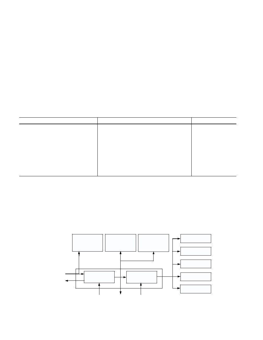
ADSP-21161N
20
REV. A
TIMING SPECIFICATIONS
The ADSP-21161N's internal clock switches at higher frequen-
cies than the system input clock (CLKIN). To generate the
internal clock, the DSP uses an internal phase-locked loop
(PLL). This PLL-based clocking minimizes the skew between
the system clock (CLKIN) signal and the DSP's internal clock
(the clock source for the external port logic and I/O pads).
The ADSP-21161N's internal clock (a multiple of CLKIN)
provides the clock signal for timing internal memory, processor
core, link ports, serial ports, and external port (as required for
read/write strobes in asynchronous access mode). During reset,
program the ratio between the DSP's internal clock frequency
and external (CLKIN) clock frequency with the CLK_CFG10
and
CLKDBL pins. Even though the internal clock is the clock
source for the external port, it behaves as described in the Clock
Rate Ratio chart in
Table 3 on Page 17
. To determine switching
frequencies for the serial and link ports, divide down the internal
clock, using the programmable divider control of each port
(DIVx for the serial ports and LxCLKD for the link ports).
Note the following definitions of various clock periods that are a
function of CLKIN and the appropriate ratio control.
Figure 10
enables Core-to-CLKIN ratios of 2:1, 3:1, 4:1, 6:1,
and 8:1 with external oscillator or crystal. It also shows support
for CLKOUT-to-CLKIN ratios of 1:1 and 2:1.
Table 5. CLKOUT and CCLK Clock Generation Operation
Timing Requirements
Description
1
Calculation
CLKIN Input
Clock
1/t
CK
CLKOUT
External Port System Clock
1/t
CKOP
PLLICLK
PLL Input Clock
1/t
PLLIN
CCLK
Core Clock
1/t
CCLK
t
CK
CLKIN Clock Period
1/CLKIN
t
CCLK
(Processor) Core Clock Period
1/CCLK
t
LCLK
Link Port Clock Period
(t
CCLK
)
×
LR
t
SCLK
Serial Port Clock Period
(t
CCLK
)
×
SR
t
SDK
SDRAM Clock Period
(t
CCLK
)
×
SDCKR
t
SPICLK
SPI Clock Period
(t
CCLK
)
×
SPIR
1
where:
LR = link port-to-core clock ratio (1, 2, 3, or 1:4, determined by LxCLKD)
SR = serial port-to-core clock ratio (wide range, determined by CLKDIV)
SDCKR = SDRAM-to-Core Clock Ratio (1:1 or 1:2, determined by SDCTL register)
SPIR = SPI-to-Core Clock Ratio (wide range, determined by SPICTL register)
LCLK = Link Port Clock
SCLK = Serial Port Clock
SDK = SDRAM Clock
SPICLK = SPI Clock
Figure 10. Core Clock and System Clock Relationship to CLKIN
CLOCK DOUBLER
1,
2
RATIOS
2,
3,
4
PLL
ASYNCHRONOUS EP
HOST
SRAM
SYNCHRONOUS EP
MULTIPROCESSING
SBSRAM
HARDWARE
INTERRUPT
I/O FLAG
TIMER
P
L
L
I
C
L
K
(
4
.
2
5
0
M
H
z
)
CLKDBL
CLKOUT
CLK_CFG10
CLKIN
(CRYSTAL OSCILLATOR
4.250MHz)
XTAL
(QUARTZ CRYSTAL
25MHz MAX)
CORE
I/O PROCESSOR
SPI
1/8 MAX
SERIAL PORTS
1/2 MAX
SDRAM
1,
1/2
LINK PORTS
1,
1/2,
1/3,
1/4
C
C
L
K
(
3
3
.
3
1
0
0
M
H
z
)

21
REV. A
ADSP-21161N
Use the exact timing information given. Do not attempt to derive
parameters from the addition or subtraction of others. While
addition or subtraction would yield meaningful results for an
individual device, the values given in this data sheet reflect sta-
tistical variations and worst cases. Consequently, it is not
meaningful to add parameters to derive longer times.
See
Figure 40 on Page 51
under Test Conditions for voltage
reference levels.
Switching characteristics specify how the processor changes its
signals. Circuitry external to the processor must be designed for
compatibility with these signal characteristics. Switching charac-
teristics describe what the processor will do in a given circum-
stance. Use switching characteristics to ensure that any timing
requirement of a device connected to the processor (such as
memory) is satisfied.
Timing requirements apply to signals that are controlled by
circuitry external to the processor, such as the data input for a
read operation. Timing requirements guarantee that the
processor operates correctly with other devices.
Power Dissipation
Total power dissipation has two components: one due to internal
circuitry and one due to the switching of external output drivers.
Internal power dissipation depends on the instruction execution
sequence and the data operands involved. Using the current spec-
ifications (I
DDINPEAK
, I
DDINHIGH
, I
DDINLOW
, I
DDIDLE
) from the
Electrical Characteristics
on Page 18
and the current-versus-
operation information in
Table 6
, the programmer can estimate
the ADSP-21161N's internal power supply (V
DDINT
) input
current for a specific application, according to the following
formula:
The external component of total power dissipation is caused by
the switching of output pins. Its magnitude depends on:
·
The number of output pins that switch during each cycle
(O)
·
The maximum frequency at which they can switch (f)
·
Their load capacitance (C)
·
Their voltage swing (V
DD
)
and is calculated by:
The load capacitance should include the processor package
capacitance (C
IN
). The switching frequency includes driving the
load high and then back low. At a maximum rate of 1/t
CK
,
address and data pins can drive high and low, while writing to a
SDRAM memory.
Example: Estimate P
EXT
with the following assumptions:
·
A system with one bank of external memory (32 bit)
·
Two 1M 16 SDRAM chips are used, each with a load
of 10 pF (ignoring trace capacitance)
·
External Data Memory writes can occur every cycle at a
rate of 1/t
CK
with 50% of the pins switching
·
The bus cycle time is 50 MHz
·
The external SDRAM clock rate is 100 MHz
·
Ignoring SDRAM refresh cycles
·
Addresses are incremental and on the same page
The P
EXT
equation is calculated for each class of pins that can
drive, as shown in
Table 7
.
A typical power consumption can now be calculated for these
conditions by adding a typical internal power dissipation:
Where:
P
EXT
is from
Table 7
.
P
INT
is I
DDINT
× 1.8 V, using the calculation I
DDINT
listed in
Power
Dissipation on Page 21
.
P
PLL
is AI
DD
× 1.8 V, using the value for AI
DD
listed in the Electrical
Characteristics
on Page 18
.
% Peak
I
DDINPEAK
×
% High
I
DDINHIGH
×
% Low
I
DDINLOW
×
+ % Idle
I
DDIDLE
×
I
DDINT
--------------------------------------------------
Table 6. Operation Types Versus Input Current
Operation
Peak Activity
1
(I
DDINPEAK
)
High Activity
1
(I
DDINHIGH
)
Low Activity
1
(I
DDINLOW
)
Instruction Type
Multifunction
Multifunction
Single Function
Instruction Fetch
Cache
Internal Memory
Internal Memory
Core Memory Access
2
2 per t
CK
cycle (DM
×
64 and PM
×
64)
1 per t
CK
cycle (DM
×
64)
None
Internal Memory DMA
1 per 2 t
CCLK
cycles
1 per 2 t
CCLK
cycles
N/A
External Memory DMA
1 per external port cycle (
×
32)
1 per external port cycle (
×
32)
N/A
Data bit pattern for core
memory access and DMA
Worst case
Random
N/A
1
The state of the PEYEN bit (SIMD versus SISD mode) does not influence these calculations.
2
These assume a 2:1 core clock ratio. For more information on ratios and clocks (t
CK
and t
CCLK
), see the timing ratio definitions
on Page 20
.
P
EXT
O
C
×
V
DD
2
×
f
×
=
P
TOTAL
P
EXT
P
INT
P
PLL
+
+
=
ADSP-21161N
22
REV. A
Note that the conditions causing a worst-case P
EXT
are different
from those causing a worst-case P
INT
. Maximum P
INT
cannot
occur while 100% of the output pins are switching from all ones
to all zeros. Note also that it is not common for an application to
have 100% or even 50% of the outputs switching simultaneously.
Power-Up Sequencing Silicon Revision 0.3, 1.0, 1.1
The timing requirements for DSP startup for silicon revision 0.3,
1.0, or 1.1 are given in
Table 8
.
Table 7. External Power Calculations (3.3 V Device)
Pin Type
Number of Pins
% Switching
C
f
V
DD
2
= P
EXT
Address
11
20
24.7 pF
50 MHz
10.9 V
= 0.030 W
MSx
4
0
24.7 pF
N/A
10.9 V
= 0.000 W
SDWE
1
0
24.7 pF
N/A
10.9 V
= 0.000 W
Data
32
50
14.7 pF
50 MHz
10.9 V
= 0.128 W
SDCLK0
1
100
24.7 pF
100 MHz
10.9 V
= 0.027 W
P
EXT
= 0.185 W
Table 8. Power-Up Sequencing for Revisions 0.3, 1.0, and 1.1 (DSP Startup)
Parameter
Min
Max
Unit
Timing Requirements
t
RSTVDD
RESET Low Before V
DDINT
/V
DDEXT
on
0
ns
t
VDDRAMP
V
DDINT
/V
DDEXT
Voltage Ramp Rate
1
0.0009
9
V/µs
t
IVDDEVDD
V
DDINT
on Before V
DDEXT
50
+200
ms
t
CLKVDD
CLKIN Valid After V
DDINT
/V
DDEXT
Valid
0
200
ms
t
VDDRST
V
DDINT
/V
DDEXT
Valid Before
RESET Deasserted
2
100
µs
t
CLKRST
CLKIN Valid Before
RESET Deasserted
3
100
µs
t
PLLRST
PLL Control Setup Before
RESET Deasserted
20
µs
1
The minimum 0.9 V/ms is based on the slowest allowable ramp-up time (2 ms) for V
DDINT
to ramp from 0 volts to 1.8 volts and (3.6 ms) for V
DDEXT
to
ramp from 0 volts to 3.3 volts.
2
The minimum time of 0 ns assumes that V
DDINT
and V
DDEXT
power supplies are valid. The V
DDINT
and V
DDEXT
supplies must be fully ramped to their
1.8 and 3.3 volt rails before
RESET can be deasserted.
3
The 100 µs minimum assumes a stable CLKIN signal after meeting worst-case start-up timing of crystal oscillator circuits. Refer to the crystal oscillator
manufacturer's data sheet for start-up time. A 25 ms maximum oscillator start-up time can be assumed if using the XTAL pin and internal oscillator
circuit in conjunction with an external crystal. 100 µs is the minimum time required for the PLL to reliably lock to a valid (stable) CLKIN frequency.
Figure 11. Power-Up Sequencing for Revisions 0.3, 1.0, and 1.1 (DSP Startup)
RESET
CLKDBL
CLK_CFG1-0
CLKIN
t
RSTVDD
VDDEXT
VDDINT
t
CLKRST
t
VDDRAMP
t
IVDDEVDD
t
VDDRAMP
t
PLLRST
t
CLKVDD
t
VDDRST
23
REV. A
ADSP-21161N
Power-Up Sequencing Silicon Revision 1.2
The timing requirements for DSP startup for silicon with revision
1.2 are given in
Table 9
.
RSTOUT does not currently exist for ADSP-21161N revisions
0.3, 1.0, and 1.1. This new signal will be placed on one of the
current no-connect pins: ball B15.
During the power-up sequence of the DSP, differences in the
ramp-up rates and activation time between the two supplies can
cause current to flow in the I/O ESD protection circuitry. To
prevent damage to the ESD diode protection circuitry, Analog
Devices recommends including a bootstrap Schottky diode.
The bootstrap Schottky diode is connected between the 1.8 V
and 3.3 V power supplies as shown in
Figure 13
. It protects the
ADSP-21161N from partially powering the 3.3 V supply.
Including a Schottky diode will shorten the delay between
the supply ramps and thus prevent damage to the ESD diode
Table 9. Power-Up Sequencing for Revision 1.2 (DSP Startup)
Parameter
Min
Max
Unit
Timing Requirements
t
RSTVDD
RESET Low Before V
DDINT
/V
DDEXT
on
0
ns
t
IVDDEVDD
V
DDINT
on Before V
DDEXT
50
+200
ms
t
CLKVDD
CLKIN Valid After V
DDINT
/V
DDEXT
Valid
1
0
200
ms
t
CLKRST
CLKIN Valid Before
RESET Deasserted
2
10
µs
t
PLLRST
PLL Control Setup Before
RESET Deasserted
3
20
µs
t
WRST
Subsequent
RESET Low Pulsewidth
4
4t
CK
ns
Switching Requirements
t
CORERST
DSP core reset deasserted after
RESET deasserted
4080t
CK
3, 5
1
Valid V
DDINT
/V
DDEXT
assumes that the supplies are fully ramped to their 1.8 and 3.3 volt rails. Voltage ramp rates can vary from microseconds to hundreds
of milliseconds depending on the design of the power supply subsystem.
2
Assumes a stable CLKIN signal, after meeting worst-case start-up timing of crystal oscillators. Refer to the crystal oscillator manufacturer's data sheet for
start-up time. Assume a 25 ms maximum oscillator start-up time if using the XTAL pin and internal oscillator circuit in conjunction with an external crystal.
3
Based on CLKIN cycles
4
Applies after the power-up sequence is complete. Subsequent resets require a minimum of 4 CLKIN cycles for
RESET to be held low in order to properly
initialize and propagate default states at all I/O pins.
5
The 4080 cycle count depends on t
SRST
specification in
Table 11
. If setup time is not met, one additional CLKIN cycle may be added to the core reset
time, resulting in 4081 cycles maximum.
Figure 12. Power-Up Sequencing for Revision 1.2 (DSP Startup)
RESET
RSTOUT
CLKDBL
CLK_CFG1-0
CLKIN
t
RSTVDD
VDDEXT
VDDINT
t
PLLRST
t
CLKRST
t
CLKVDD
t
IVDDEVDD
t
CORERST
ADSP-21161N
24
REV. A
protection circuitry. With this technique, if the 1.8 V rail rises
ahead of the 3.3 V rail, the Schottky diode pulls the 3.3 V rail
along with the 1.8 V rail.
Clock Input
In systems that use multiprocessing or SBSRAM,
CLKDBL
cannot be enabled nor can the systems use an external crystal as
the CLKIN source.
Do not use CLKOUT as the clock source for the SBSRAM
device. Using an external crystal in conjunction with
CLKDBL
to generate a CLKOUT frequency is not supported. Negative
hold times can result from the potential skew between CLKIN
and CLKOUT.
Clock Signals
The ADSP-21161N can use an external clock or a crystal. See
CLKIN pin description. The programmer can configure the
ADSP-21161N to use its internal clock generator by connecting
the necessary components to CLKIN and XTAL.
Figure 15
shows the component connections used for a crystal operating in
fundamental mode.
Figure 13. Dual Voltage Schottky Diode
3.3V I/O
VOLTAGE
REGULATOR
1.8V CORE
VOLTAGE
REGULATOR
V
DDEXT
V
DDINT
ADSP-21161N
DC INPUT
SOURCE
Table 10. Clock Input
Parameter
100 MHz
Unit
Min
Max
Timing Requirements
t
CK
CLKIN Period
1
20
238
ns
t
CKL
CLKIN Width Low
1
7.5
119
ns
t
CKH
CLKIN Width High
1
7.5
119
ns
t
CKRF
CLKIN Rise/Fall (0.4 V2.0 V)
3
ns
t
CCLK
CCLK Period
10
30
ns
Switching Characteristics
t
DCKOO
CLKOUT Delay After CLKIN
0
2
ns
t
CKOP
CLKOUT Period
t
CKOP
1
t
CKOP
+1
ns
t
CKWH
CLKOUT Width High
t
CKOP
/2 2
t
CKOP
/2 + 2
ns
t
CKWL
CLKOUT Width Low
t
CKOP
/2 2
t
CKOP
/2 + 2
ns
1
CLKIN is dependent on the configuration of the CLKCFGx and
CLKDBL pins to achieve desired t
CCLK
.
Figure 14. Clock Input
CLKIN
t
CKH
t
CK
t
CKL
CLKOUT
t
DCKOO
1
t
CKOP
1
t
CKWL
1
t
CKWH
1
CLKOUT
NOTES:
1. WHEN
CLKDBL
IS DISABLED, ANY SPECIFICATION TO CLKIN
APPLIES TO THE RISING EDGE, ONLY.
2. WHEN
CLKDBL
IS ENABLED, ANY SPECIFICATION TO CLKIN
APPLIES TO THE RISING OR FALLING EDGE.
t
DCKOO
2
t
CKOP
2
t
DCKOO
2
t
CKWH
2
t
CKWL
2
Figure 15. 100 MHz Operation (Fundamental Mode
Crystal)
CLKIN
XTAL
C2
27pF
C1
27pF
X1
SUGGESTED COMPONENTS FOR 100MHz OPERATION:
ECLIPTEK EC2SM-25.000M (SURFACE MOUNT PACKAGE)
ECLIPTEK EC-25.000M (THROUGH-HOLE PACKAGE)
C1 = 27pF
C2 = 27pF
NOTE: C1 AND C2 ARE SPECIFIC TO CRYSTAL SPECIFIED FOR X1.
CONTACT CRYSTAL MANUFACTURER FOR DETAILS. THIS 25MHz
CRYSTAL GENERATES A 100MHz CCLK AND A 50MHz EP CLOCK
WITH
CLKDBL
ENABLED AND A 2:1 PLL MULTIPLY RATIO.
25
REV. A
ADSP-21161N
Reset
Interrupts
Table 11. Reset
Parameter
Min
Max
Unit
Timing Requirements
t
WRST
RESET Pulsewidth Low
1
4t
CK
ns
t
SRST
RESET Setup Before CLKIN High
2
8.5
ns
1
Applies after the power-up sequence is complete.
2
Only required if multiple ADSP-21161Ns must come out of reset synchronous to CLKIN with program counters (PC) equal. Not required for multiple
ADSP-21161Ns communicating over the shared bus (through the external port), because the bus arbitration logic synchronizes itself automatically
after reset.
Figure 16. Reset
RESET
CLKIN
t
WRST
t
SRST
Table 12. Interrupts
Parameter
Min
Max
Unit
Timing Requirements
t
SIR
IRQ20 Setup Before CLKIN
1
6
ns
t
HIR
IRQ20 Hold After CLKIN
1
0
ns
t
IPW
IRQ20 Pulsewidth
2
2 + t
CKOP
ns
1
Only required for
IRQx recognition in the following cycle.
2
Applies only if t
SIR
and t
HIR
requirements are not met.
Figure 17. Interrupts
CLKIN
t
IPW
t
SIR
t
HIR
IRQ20
ADSP-21161N
26
REV. A
Timer
Flags
Table 13. Timer
Parameter
Min
Max Unit
Switching Characteristic
t
DTEX
CLKIN to TIMEXP
1
7
ns
Figure 18. Timer
CLKIN
TIMEXP
t
DTEX
t
DTEX
Table 14. Flags
Parameter
Min
Max
Unit
Timing Requirement
t
SFI
FLAG110
IN
Setup Before CLKIN
1
4
ns
t
HFI
FLAG110
IN
Hold After CLKIN
1
1
ns
t
DWRFI
FLAG110
IN
Delay After
RD/WR Low
1
12
ns
t
HFIWR
FLAG110
IN
Hold After
RD/WR Deasserted
1
0
ns
Switching Characteristics
t
DFO
FLAG110
OUT
Delay After CLKIN
9
ns
t
HFO
FLAG110
OUT
Hold After CLKIN
1
ns
t
DFOE
CLKIN to FLAG110
OUT
Enable
1
ns
t
DFOD
CLKIN to FLAG110
OUT
Disable
5
ns
1
Flag inputs meeting these setup and hold times for instruction cycle N will affect conditional instructions in instruction cycle N+2.
Figure 19. Flags
CLKIN
FLAG110
OUT
FLAG OUTPUT
CLKIN
FLAG INPUT
FLAG110
IN
t
DFO
t
HFO
t
DFO
t
DFOD
t
DFOE
t
SFI
t
HFI
t
HFIWR
t
DWRFI
RD WR
,
27
REV. A
ADSP-21161N
Memory Read Bus Master
Use these specifications for asynchronous interfacing to
memories (and memory-mapped peripherals) without reference
to CLKIN. These specifications apply when the ADSP-21161N
is the bus master accessing external memory space in asynchro-
nous access mode.
Table 15. Memory Read
Bus Master
Parameter
Min
Max
Unit
Timing Requirements
t
DAD
Address, Selects Delay to Data Valid
1, 2
t
CKOP
0.25t
CCLK
11+ W
ns
t
DRLD
RD Low to Data Valid
1
0.75t
CKOP
11 + W
ns
t
HDA
Data Hold from Address, Selects
3
0
ns
t
SDS
Data Setup to
RD High
8
ns
t
HDRH
Data Hold from
RD High
3
1
ns
t
DAAK
ACK Delay from Address, Selects
2, 4
t
CKOP
0.5t
CCLK
12 + W
ns
t
DSAK
ACK Delay from
RD Low
4
t
CKOP
0.75t
CCLK
11 + W
ns
t
SAKC
ACK Setup to CLKIN
4
0.5t
CCLK
+3
ns
t
HAKC
ACK Hold After CLKIN
1
ns
Switching Characteristics
t
DRHA
Address Selects Hold After
RD High
0.25t
CCLK
1+ H
ns
t
DARL
Address Selects to
RD Low
2
0.25t
CCLK
3
ns
t
RW
RD Pulsewidth
t
CKOP
0.5t
CCLK
1 + W
ns
t
RWR
RD High to WR, RD, DMAGx Low
0.5t
CCLK
1 + HI
ns
W = (number of wait states specified in WAIT register) × t
CKOP
.
HI = t
CKOP
(if an address hold cycle or bus idle cycle occurs, as specified in WAIT register; otherwise HI = 0).
H = t
CKOP
(if an address hold cycle occurs as specified in WAIT register; otherwise H = 0).
1
Data Delay/Setup: User must meet t
DAD
, t
DRLD
, or t
SDS.
2
The falling edge of
MSx, BMS is referenced.
3
Data Hold: User must meet t
HDA
or t
HDRH
in asynchronous access mode. See
Example System Hold Time Calculation on Page 51
for the calculation of
hold times given capacitive and dc loads.
4
ACK Delay/Setup: User must meet t
DAAK
, t
DSAK
, or t
SAKC
for deassertion of ACK (Low); all three specifications must be met for assertion of ACK (High).
Figure 20. Memory Read Bus Master
ACK
DATA
t
DARL
t
RW
t
DAD
t
DAAK
t
HDRH
t
HDA
t
RWR
t
DRLD
t
DRHA
t
DSAK
t
SDS
t
SAKC
t
HAKC
CLKIN
ADDRESS
MSx
,
BMS
RD
WR
,
DMAG
ADSP-21161N
28
REV. A
Memory Write Bus Master
Use these specifications for asynchronous interfacing to
memories (and memory-mapped peripherals) without reference
to CLKIN. These specifications apply when the ADSP-21161N
is the bus master accessing external memory space in asynchro-
nous access mode.
Table 16. Memory Write Bus Master
Parameter
Min
Max
Unit
Timing Requirements
t
DAAK
ACK Delay from Address, Selects
1, 2
t
CKOP
0.5t
CCLK
12+W
ns
t
DSAK
ACK Delay from
WR Low
1
t
CKOP
0.75t
CCLK
11+W
ns
t
SAKC
ACK Setup to CLKIN
1
0.5t
CCLK
+ 3
ns
t
HAKC
ACK Hold After CLKIN
1
1
ns
Switching Characteristics
t
DAWH
Address, Selects to
WR Deasserted
2
t
CKOP
0.25t
CCLK
3 + W
ns
t
DAWL
Address, Selects to
WR Low
2
0.25t
CCLK
3
ns
t
WW
WR Pulsewidth
t
CKOP
0.5t
CCLK
1 + W
ns
t
DDWH
Data Setup Before
WR High
t
CKOP
0.25t
CCLK
13.5 + W
ns
t
DWHA
Address Hold After
WR Deasserted
0.25t
CCLK
1 + H
ns
t
DWHD
Data Hold After
WR Deasserted
0.25t
CCLK
1 + H
ns
t
DATRWH
Data Disable After
WR Deasserted
3
0.25t
CCLK
2 + H
0.25t
CCLK
+2.5+H
ns
t
WWR
WR High to WR, RD, DMAGx Low
0.5t
CCLK
1.25 + HI
ns
t
DDWR
Data Disable Before
WR or RD Low
0.25t
CCLK
3 + I
ns
t
WDE
WR Low to Data Enabled
0.25t
CCLK
1
ns
W = (number of wait states specified in WAIT register) × t
CKOP
.
H = t
CKOP
(if an address hold cycle occurs, as specified in WAIT register; otherwise H = 0).
HI = t
CKOP
(if an address hold cycle or bus idle cycle occurs, as specified in WAIT register; otherwise HI = 0).
I = t
CKOP
(if a bus idle cycle occurs, as specified in WAIT register; otherwise I = 0).
1
ACK Delay/Setup: User must meet t
DAAK
or t
DSAK
or t
SAKC
for deassertion of ACK (Low); all three specifications must be met for assertion of ACK (High).
2
The falling edge of
MSx, BMS is referenced.
3
See
Example System Hold Time Calculation on Page 51
for calculation of hold times given capacitive and dc loads.
Figure 21. Memory Write Bus Master
t
DATRWH
ACK
DATA
t
DAWL
t
WW
t
DAAK
t
WWR
t
WDE
t
DDWR
t
DWHA
t
DAWH
t
DSAK
t
DDWH
t
DWHD
t
SAKC
t
HAKC
CLKIN
ADDRESS
MSx
,
BMS
WR
RD
,
DMAG
29
REV. A
ADSP-21161N
Synchronous Read/Write Bus Master
Use these specifications for interfacing to external memory
systems that require CLKIN, relative to timing or for accessing
a slave ADSP-21161N (in multiprocessor memory space). When
accessing a slave ADSP-21161N, these switching characteristics
must meet the slave's timing requirements for synchronous
read/writes (see
Synchronous Read/Write Bus Slave on
Page 30
). The slave ADSP-21161N must also meet these (bus
master) timing requirements for data and acknowledge setup and
hold times.
Table 17. Synchronous Read/Write Bus Master
Parameter
Min
Max
Unit
Timing Requirements
t
SSDATI
Data Setup Before CLKIN
5.5
ns
t
HSDATI
Data Hold After CLKIN
1
ns
t
SACKC
ACK Setup Before CLKIN
0.5t
CCLK
+3
ns
t
HACKC
ACK Hold After CLKIN
1
ns
Switching Characteristics
t
DADDO
Address,
MSx, BMS, BRST, Delay After CLKIN
10
ns
t
HADDO
Address,
MSx, BMS, BRST, Hold After CLKIN
1.5
ns
t
DRDO
RD High Delay After CLKIN
0.25t
CCLK
1
0.25t
CCLK
+9
ns
t
DWRO
WR High Delay After CLKIN
0.25t
CCLK
1
0.25t
CCLK
+9
ns
t
DRWL
RD/WR Low Delay After CLKIN
0.25t
CCLK
1
0.25t
CCLK
+9
ns
t
DDATO
Data Delay After CLKIN
12.5
ns
t
HDATO
Data Hold After CLKIN
1.5
ns
Figure 22. Synchronous Read/Write Bus Master
CLKIN
ACK
(IN)
DATA (OUT)
DATA
(IN)
WRITE CYCLE
READ CYCLE
t
DRWL
t
HSDATI
t
SSDATI
t
DRDO
t
DWRO
t
HDATO
t
DDATO
t
DRWL
t
SACKC
t
HACKC
t
HADDO
t
DADDO
ADDRESS
MSx
,
BRST
RD
WR
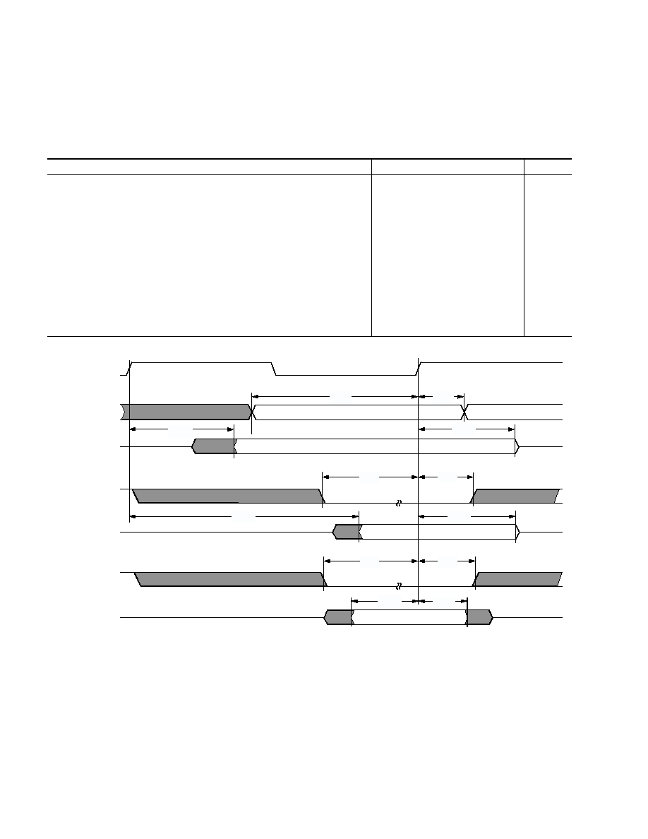
ADSP-21161N
30
REV. A
Synchronous Read/Write Bus Slave
Use these specifications for ADSP-21161N bus master accesses
of a slave's IOP registers in multiprocessor memory space. The
bus master must meet these (bus slave) timing requirements.
Table 18. Synchronous Read/Write Bus Slave
Parameter
Min
Max
Unit
Timing Requirements
t
SADDI
Address, BRST Setup Before CLKIN
5
ns
t
HADDI
Address, BRST Hold After CLKIN
1
ns
t
SRWI
RD/WR Setup Before CLKIN
5
ns
t
HRWI
RD/WR Hold After CLKIN
1
ns
t
SSDATI
Data Setup Before CLKIN
5.5
ns
t
HSDATI
Data Hold After CLKIN
1
ns
Switching Characteristics
t
DDATO
Data Delay After CLKIN
12.5
ns
t
HDATO
Data Hold After CLKIN
1.5
ns
t
DACKC
ACK Delay After CLKIN
10
ns
t
HACKO
ACK Hold After CLKIN
1.5
ns
Figure 23. Synchronous Read/Write Bus Slave
CLKIN
ADDRESS
ACK
DATA
(OUT)
WRITE ACCESS
DATA
(IN)
READ ACCESS
t
SADDI
t
HADDI
t
DACKC
t
HACKO
t
HRWI
t
SRWI
t
DDATO
t
HDATO
t
SRWI
t
HRWI
t
HSDATI
t
SSDATI
RD
WR
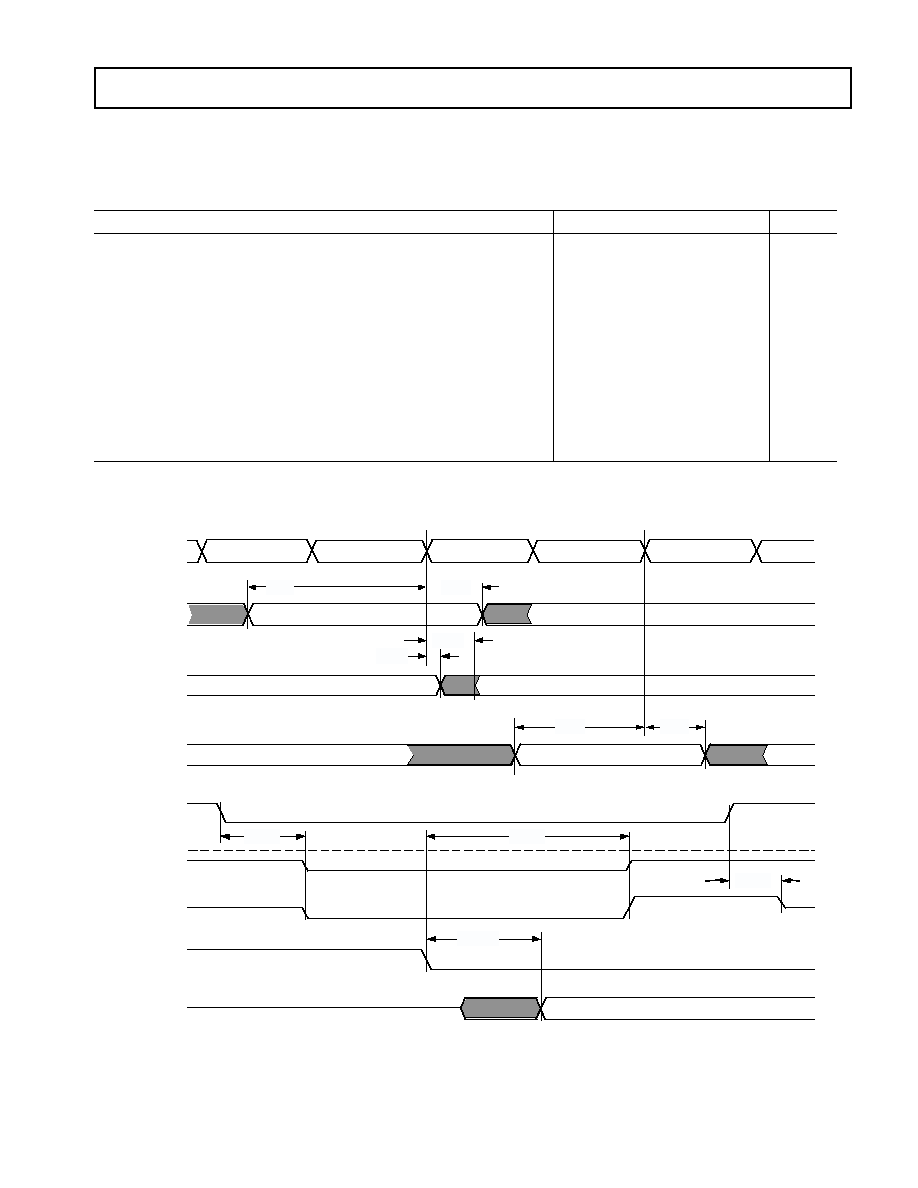
31
REV. A
ADSP-21161N
Host Bus Request
Use these specifications for asynchronous host bus requests of an
ADSP-21161N (
HBR, HBG).
Table 19. Host Bus Request
Parameter
Min
Max
Unit
Timing Requirements
t
HBGRCSV
HBG Low to RD/WR/CS Valid
19
ns
t
SHBRI
HBR Setup Before CLKIN
1
6
ns
t
HHBRI
HBR Hold After CLKIN
1
1
ns
t
SHBGI
HBG Setup Before CLKIN
6
ns
t
HHBGI
HBG Hold After CLKIN
1
ns
Switching Characteristics
t
DHBGO
HBG Delay After CLKIN
7
ns
t
HHBGO
HBG Hold After CLKIN
1.5
ns
t
DRDYCS
REDY (O/D) or (A/D) Low from
CS and HBR Low
2
10
ns
t
TRDYHG
REDY (O/D) Disable or REDY (A/D) High from
HBG
2
t
CKOP
+14
ns
t
ARDYTR
REDY (A/D) Disable from
CS or HBR High
2
11
ns
1
Only required for recognition in the current cycle.
2
(O/D) = open drain, (A/D) = active drive.
Figure 24. Host Bus Request
REDY
(O/D)
REDY
(A/D)
O/D = OPEN DRAIN, A/ D = ACTIVE DRIVE
t
D R DY C S
t
H B GR CS V
t
TR D YH G
t
A R D YTR
t
SH B GI
t
H H B GI
CLKIN
(OUT)
HBG
t
H H BR I
t
SH B R I
t
H H B GO
t
D H BG O
HBR
(IN)
HBG
HBR
CS
(OUT)
HBG
RD
WR
CS
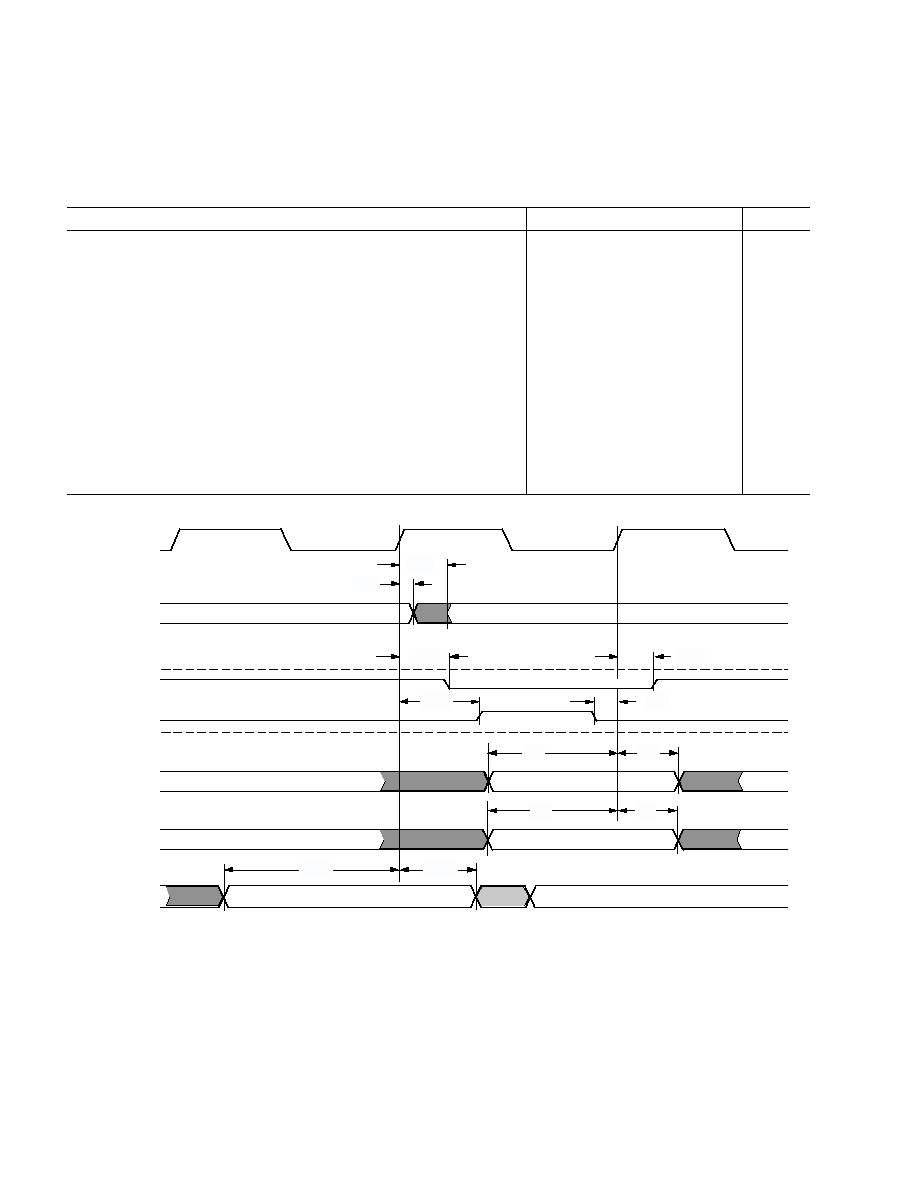
ADSP-21161N
32
REV. A
Multiprocessor Bus Request
Use these specifications for passing of bus mastership between
multiprocessing ADSP-21161Ns (
BRx).
Table 20. Multiprocessor Bus Request
Parameter
Min
Max
Unit
Timing Requirements
t
SBRI
BRx, Setup Before CLKIN High
9
ns
t
HBRI
BRx, Hold After CLKIN High
0.5
ns
t
SPAI
PA Setup Before CLKIN High
9
ns
t
HPAI
PA Hold After CLKIN High
1
ns
t
SRPBAI
RPBA Setup Before CLKIN High
6
ns
t
HRPBAI
RPBA Hold After CLKIN High
2
ns
Switching Characteristics
t
DBRO
BRx Delay After CLKIN High
8
ns
t
HBRO
BRx Hold After CLKIN High
1.0
ns
t
DPASO
PA Delay After CLKIN High, Slave
8
ns
t
TRPAS
PA Disable After CLKIN High, Slave
1.5
ns
t
DPAMO
PA Delay After CLKIN High, Master
0.25t
CCLK
+9
ns
t
PATR
PA Disable Before CLKIN High, Master
0.25t
CCLK
5
ns
Figure 25. Multiprocessor Bus Request
t
H BR I
RPBA
O/D = OPEN DRAI N
t
HR P B AI
t
S R PB A I
t
SB R I
CLKIN
PA
(OUT)
(SLAVE)
t
D B RO
t
H B RO
t
DP A SO
t
TR PA S
PA
(OUT)
(MASTER)
t
D PA MO
t
P AT R
PA
(IN)
(O/D)
t
H PA I
t
S PA I
BRx
(OUT)
BRx
(IN)

33
REV. A
ADSP-21161N
Asynchronous Read/Write Host to ADSP-21161N
Use these specifications for asynchronous host processor accesses
of an ADSP-21161N, after the host has asserted
CS and HBR
(low). After
HBG is returned by the ADSP-21161N, the host can
drive the
RD and WR pins to access the ADSP-21161N's IOP
registers.
HBR and HBG are assumed low for this timing.
Although the DSP will recognize
HBR asserted before reset, a
HBG will not be returned by the DSP until after reset is deas-
serted and the DSP completes bus synchronization.
Note: Host internal memory access is not supported.
Table 21. Read Cycle
Parameter
Min
Max
Unit
Timing Requirements
t
SADRDL
Address Setup and
CS Low Before RD Low
0
ns
t
HADRDH
Address Hold and
CS Hold Low After RD
2
ns
t
WRWH
RD/WR High Width
3.5
ns
t
DRDHRDY
RD High Delay After REDY (O/D) Disable
0
ns
t
DRDHRDY
RD High Delay After REDY (A/D) Disable
0
ns
Switching Characteristics
t
SDATRDY
Data Valid Before REDY Disable from Low
2
ns
t
DRDYRDL
REDY (O/D) or (A/D) Low Delay After
RD Low
10
ns
t
RDYPRD
REDY (O/D) or (A/D) Low Pulsewidth for Read
1.5t
CCLK
ns
t
HDARWH
Data Disable After
RD High
2
6
ns
Table 22. Write Cycle
Parameter
Min
Max
Unit
Timing Requirements
t
SCSWRL
CS Low Setup Before WR Low
0
ns
t
HCSWRH
CS Low Hold After WR High
0
ns
t
SADWRH
Address Setup Before
WR High
6
ns
t
HADWRH
Address Hold After
WR High
2
ns
t
WWRL
WR Low Width
t
CCLK
+1
ns
t
WRWH
RD/WR High Width
3.5
ns
t
DWRHRDY
WR High Delay After REDY (O/D) or (A/D) Disable
0
ns
t
SDATWH
Data Setup Before
WR High
5
ns
t
HDATWH
Data Hold After
WR High
4
ns
Switching Characteristics
t
DRDYWRL
REDY (O/D) or (A/D) Low Delay After
WR/CS Low
1
11
ns
t
RDYPWR
REDY (O/D) or (A/D) Low Pulsewidth for Write
1
12
ns
1
Only when slave write FIFO is full.
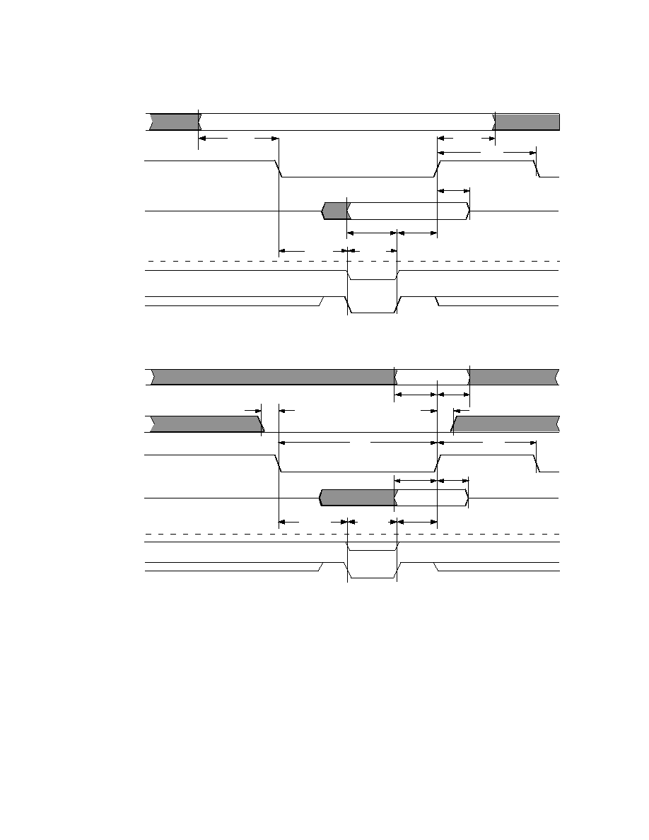
ADSP-21161N
34
REV. A
Figure 26. Asynchronous Read/Write Host to ADSP-21161N
REDY (O/D)
READ CYCLE
DATA (OUT)
REDY (A/D)
O/D = OPEN DRAI N, A/D = ACTIVE DRIVE
REDY (O/D)
WRITE CYCLE
DATA (IN)
ADDRESS
REDY (A/D)
t
D RDY R DL
t
H D AR W H
t
R DYPRD
t
D R DH RD Y
t
S D AT RD Y
t
SDA TWH
t
H D ATWH
t
D R DY WR L
t
H A DW RH
t
RD YPW R
t
DWR H R D Y
t
S A DW R H
t
SC S WRL
t
HC SWR H
t
H A D RD H
t
WR WH
t
WWRL
t
W RW H
t
SA D R DL
RD
CS
WR
ADDRESS/
CS

35
REV. A
ADSP-21161N
Three-State Timing Bus Master, Bus Slave
These specifications show how the memory interface is disabled
(stops driving) or enabled (resumes driving) relative to CLKIN
and the
SBTS pin. This timing is applicable to bus master tran-
sition cycles (BTC) and host transition cycles (HTC) as well as
the
SBTS pin.
During reset, the DSP will not respond to
SBTS, HBR, and
MMS accesses. Although the DSP will recognize
HBR asserted
before reset, a
HBG will not be returned by the DSP until after
reset is deasserted and the DSP completes bus synchronization.
Table 23. Three-State Timing Bus Master, Bus Slave
Parameter
Min
Max
Unit
Timing Requirements
t
STSCK
SBTS Setup Before CLKIN
6
ns
t
HTSCK
SBTS Hold After CLKIN
2
ns
Switching Characteristics
t
MIENA
Address/Select Enable After CLKIN High
1.5
9
ns
t
MIENS
Strobes Enable After CLKIN High
1
-
1.5
+9
ns
t
MIENHG
HBG Enable After CLKIN
1.5
9
ns
t
MITRA
Address/Select Disable After CLKIN High
0.5t
CKOP
20
0.5t
CKOP
15
ns
t
MITRS
Strobes Disable After CLKIN High
t
CKOP
0.25
t
CCLK
-
17
t
CKOP
0.25
t
CCLK
-
12.5
ns
t
MITRHG
HBG Disable After CLKIN
2
0.5t
CKOP
+N
×
t
CCLK
20
0.5t
CKOP
+N
×
t
CCLK
15
ns
t
DATEN
Data Enable After CLKIN
3
1.5
10
ns
t
DATTR
Data Disable After CLKIN
3
1.5
6
ns
t
ACKEN
ACK Enable After CLKIN High
1.5
9
ns
t
ACKTR
ACK Disable After CLKIN High
0.2
5
ns
t
CDCEN
CLKOUT Enable After CLKIN
2
0.5t
CKOP
+N
×
t
CCLK
0.5t
CKOP
+N
×
t
CCLK
+5
ns
t
CDCTR
CLKOUT Disable After CLKIN
t
CKOP
-5
t
CKOP
ns
t
ATRHBG
Address/Select Disable Before
HBG Low
4
1.5t
CKOP
6
1.5t
CKOP
+2
ns
t
STRHBG
RD/WR/DMAGx Disable Before HBG Low
4
t
CKOP
+
0.25
t
CCLK
-
4
t
CKOP
+
0.25
t
CCLK
+3
ns
t
BTRHBG
BMS Disable Before HBG Low
4
0.5t
CKOP
4
0.5t
CKOP
+2
ns
t
MENHBG
Memory Interface Enable After
HBG High
4
t
CKOP
5
t
CKOP
+5
ns
1
Strobes =
RD, WR, DMAGx.
2
Where N = 0.5, 1.0, 1.5 for 1:2, 1:3, and 1:4, respectively.
3
In addition to bus master transition cycles, these specs also apply to bus master and bus slave synchronous read/write.
4
Memory Interface = Address,
RD, WR, MSx, DMAGx, and BMS (in EPROM boot mode). BMS is only an output in EPROM boot mode.
ADSP-21161N
36
REV. A
Figure 27. Three-State Timing Bus Master, Bus Slave
CLKIN
ACK
MEMORY
INTERFACE
CLKOUT
t
CDCTR
DATA
MEMORY
INTERFACE
t
MITRA,
t
MITRS,
t
MITRHG
t
HTSCK
t
CDCEN
t
MIENA,
t
MIENS,
t
MIENHG
CLKIN
t
ATRHBG,
t
STRHBG,
t
BTRHBG
t
STSCK
t
DATEN
t
ACKEN
t
DATTR
t
ACKTR
t
MENHBG
SBTS
HBG
MEMORY INTERFACE = ADDRESS,
RD
,
WR
,
MSx
,
DMAGx
,
BMS
(IN EPROM MODE)

37
REV. A
ADSP-21161N
DMA Handshake
These specifications describe the three DMA handshake modes.
In all three modes
DMAR is used to initiate transfers. For
handshake mode,
DMAG controls the latching or enabling of
data externally. For external handshake mode, the data transfer
is controlled by the ADDR230,
RD, WR, MS30, ACK, and
DMAG signals. For Paced Master mode, the data transfer is
controlled by ADDR230,
RD, WR, MS30, and ACK (not
DMAG). For Paced Master mode, the Memory Read-Bus
Master, Memory Write-Bus Master, and Synchronous
Read/Write-Bus Master timing specifications for ADDR23
0,
RD, WR, MS30, DATA4716, and ACK also apply.
Table 24. DMA Handshake
Parameter
Min
Max
Unit
Timing Requirements
t
SDRC
DMARx Setup Before CLKIN
1
3.5
ns
t
WDR
DMARx Width Low (Nonsynchronous)
2
t
CCLK
+ 4.5
ns
t
SDATDGL
Data Setup After
DMAGx Low
3
t
CKOP
0.5t
CCLK
7
ns
t
HDATIDG
Data Hold After
DMAGx High
2
ns
t
DATDRH
Data Valid After
DMARx High
3
t
CKOP
+ 3
ns
t
DMARLL
DMARx Low Edge to Low Edge
4
t
CKOP
ns
t
DMARH
DMARx Width High
2
t
CCLK
+ 4.5
ns
Switching Characteristics
t
DDGL
DMAGx Low Delay After CLKIN
0.25t
CCLK
+ 1
0.25t
CCLK
+ 9
ns
t
WDGH
DMAGx High Width
0.5t
CCLK
1 + HI
ns
t
WDGL
DMAGx Low Width
t
CKOP
0.5t
CCLK
1
ns
t
HDGC
DMAGx High Delay After CLKIN
t
CKOP
0.25t
CCLK
+ 1.0
t
CKOP
0.25t
CCLK
+ 9
ns
t
VDATDGH
Data Valid Before
DMAGx High
5
t
CKOP
0.25t
CCLK
8
t
CKOP
0.25t
CCLK
+ 5
ns
t
DATRDGH
Data Disable After
DMAGx High
6
0.25t
CCLK
3
0.25t
CCLK
+ 4
ns
t
DGWRL
WRx Low Before DMAGx Low
1.5
+2
ns
t
DGWRH
DMAGx Low Before WRx High
t
CKOP
0.5t
CCLK
2 + W
ns
t
DGWRR
WRx High Before DMAGx High
7
1.5
+2
ns
t
DGRDL
RDx Low Before DMAGx Low
1.5
+2
ns
t
DRDGH
RDx Low Before DMAGx High
t
CKOP
0.5t
CCLK
2 + W
ns
t
DGRDR
RDx High Before DMAGx High
7
1.5
+2
ns
t
DGWR
DMAGx High to WRx, RDx Low
0.5t
CCLK
2 + HI
ns
t
DADGH
Address/Select Valid to
DMAGx High
15
ns
t
DDGHA
Address/Select Hold After
DMAGx High
1
ns
W = (number of wait states specified in WAIT register)
×
t
CKOP
.
HI = t
CKOP
(if data bus idle cycle occurs, as specified in WAIT register; otherwise HI = 0).
1
Only required for recognition in the current cycle.
2
Maximum throughput using
DMARx/DMAGx handshaking equals t
WDR
+ t
DMARH
= (t
CCLK
+ 4.5) + (t
CCLK
+ 4.5) = 29 ns (34.5 MHz). This throughput
limit applies to non-synchronous access mode only.
3
t
SDATDGL
is the data setup requirement if
DMARx is not being used to hold off completion of a write. Otherwise, if DMARx low holds off completion of
the write, the data can be driven t
DATDRH
after
DMARx is brought high.
4
Use t
DMARLL
if
DMARx transitions synchronous with CLKIN. Otherwise, use t
WDR
and t
DMARH
.
5
t
VDATDGH
is valid if
DMARx is not being used to hold off completion of a read. If DMARx is used to prolong the read, then
t
VDATDGH
= t
CKOP
0.25t
CCLK
8 + (n × t
CKOP
) where n equals the number of extra cycles that the access is prolonged.
6
See
Example System Hold Time Calculation on Page 51
for calculation of hold times given capacitive and dc loads.
7
This parameter applies for synchronous access mode only.
ADSP-21161N
38
REV. A
Figure 28. DMA Handshake
CLKIN
t
SDRC
DATA
DATA
t
WDR
t
SDRC
t
DMARH
t
DMARLL
t
HDGC
t
WDGH
t
DDGL
t
VDATDGH
t
DATDRH
t
DATRDGH
t
HDATIDG
t
DGWRL
t
DGWRH
t
DGWRR
t
DGRDL
t
DRDGH
t
DGRDR
t
SDATDGL
(EXTERNAL DEVICE TO EXTERNAL MEMORY)
(EXTERNAL MEMORY TO EXTERNAL DEVICE)
TRANSFERS BETWEEN ADSP-21161N
INTERNAL MEMORY AND EXTERNAL DEVICE
TRANSFERS BETWEEN EXTERNAL DEVICE AND
EXTERNAL MEMORY
1
(EXTERNAL HANDSHAKE MODE)
t
DDGHA
ADDRESS
MSx
t
DADGH
t
WDGL
(FROM EXTERNAL DRIVE TO ADSP-21161N)
(FROM ADSP-2116x TO EXTERNAL DRIVE)
t
DGWR
DMARx
DMAGx
WR
RD
1
MEMORY READ BUS MASTER, MEMORY WRITE BUS MASTER, OR SYNCHRONOUS READ/WRITE BUS MASTER
TIMING SPECIFICATIONS FOR ADDR230,
RD
,
WR
,
MS3-0
AND ACK ALSO APPLY HERE.

39
REV. A
ADSP-21161N
SDRAM Interface Bus Master
Use these specifications for ADSP-21161N bus master accesses
of SDRAM:
SDRAM Interface Bus Slave
These timing requirements allow a bus slave to sample the bus
master's SDRAM command and detect when a refresh occurs:
Table 25. SDRAM Interface
Bus Master
Parameter
Min
Max
Unit
Timing Requirements
t
SDSDK
Data Setup Before SDCLK
2.0
ns
t
HDSDK
Data Hold After SDCLK
2.3
ns
Switching Characteristics
t
DSDK1
First SDCLK Rise Delay After CLKIN
1,
2
0.75t
CCLK
+ 1.5
0.75t
CCLK
+ 8.0
ns
t
SDK
SDCLK Period
t
CCLK
2
×
t
CCLK
ns
t
SDKH
SDCLK Width High
4
ns
t
SDKL
SDCLK Width Low
4
ns
t
DCADSDK
Command, Address, Data, Delay After
SDCLK
3
0.25t
CCLK
+2.5
ns
t
HCADSDK
Command, Address, Data, Hold After
SDCLK
3
2.0
ns
t
SDTRSDK
Data Three-State After SDCLK
4
0.5t
CCLK
+ 2.0
ns
t
SDENSDK
Data Enable After SDCLK
5
0.75t
CCLK
ns
t
SDCTR
Command Three-State After CLKIN
0.5t
CCLK
1.5
0.5t
CCLK
+ 6.0
ns
t
SDCEN
Command Enable After CLKIN
2
5
ns
t
SDSDKTR
SDCLK Three-State After CLKIN
0
3
ns
t
SDSDKEN
SDCLK Enable After CLKIN
1
4
ns
t
SDATR
Address Three-State After CLKIN
-
0.25 t
CCLK
-
5
-
0.25t
CCLK
ns
t
SDAEN
Address Enable After CLKIN
-
0.4
+7.2
ns
1
For the second, third, and fourth rising edges of SDCLK delay from CLKIN, add appropriate number of SDCLK period to the t
DSDK1
and t
SSDKC1
values,
depending upon the SDCKR value and the core clock to CLKIN ratio.
2
Subtract t
CCLK
from result if value is greater than or equal to t
CCLK
.
3
Command = SDCKE,
MSx, DQM, RAS, CAS, SDA10, and SDWE
4
SDRAM Controller adds one SDRAM CLK three-stated cycle delay on a read, followed by a write.
5
Valid when DSP transitions to SDRAM master from SDRAM slave.
Table 26. SDRAM Interface
Bus Slave
Parameter
Min
Max
Unit
Timing Requirements
t
SSDKC1
First SDCLK Rise
after CLKOUT
1, 2, 3
SDCK
t
CCLK
-
0.5t
CCLK
-
0.5
SDCKR
t
CCLK
-
0.25t
CCLK
+ 2.0
ns
t
SCSDK
Command Setup
before SDCLK
4
2
ns
t
HCSDK
Command Hold
after SDCLK
4
1
ns
1
For the second, third, and fourth rising edges of SDCLK delay from CLKOUT, add appropriate number of SDCLK period to the t
DSDK1
and t
SSDKC1
values, depending upon the SDCKR value and the Core clock to CLKOUT ratio.
2
SDCKR = 1 for SDCLK equal to core clock frequency and SDCKR = 2 for SDCLK equal to half core clock frequency.
3
Subtract t
CCLK
from result if value is greater than or equal to t
CCLK
.
4
Command = SDCKE,
RAS, CAS, and SDWE.
ADSP-21161N
40
REV. A
Figure 29. SDRAM Interface
CLKIN
SDCLK
DATA(IN)
DATA(OUT)
CMND
1
ADDR
(OUT)
CMND
1
(OUT)
ADDR
(OUT)
CLKOUT
SDCLK (IN)
CMND
2
(IN)
t
SDK
t
DSDK1
t
SDKH
t
SDKL
t
SDSDK
t
HDSDK
t
DCADSDK
t
SDENSDK
t
SDTRSDK
t
HCADSDK
t
DCADSDK
t
HCADSDK
t
SDCEN
t
SDCTR
t
SDATR
t
SDAEN
t
SSDKC1
t
SCSDK
t
HCSDK
CLKIN
t
SDSDKEN
t
SDSDKTR
SDCLK
1
COMMAND = SDCKE,
MSx
,
RAS
,
CAS
,
SDWE
, DQM, AND SDA10.
2
COMMAND = SDCKE,
RAS
,
CAS
, AND
SDWE
.
41
REV. A
ADSP-21161N
Link Ports
Calculation of link receiver data setup and hold relative to link
clock is required to determine the maximum allowable skew that
can be introduced in the transmission path between LDATA and
LCLK. Setup skew is the maximum delay that can be introduced
in LDATA relative to LCLK, (setup skew = t
LCLKTWH
min t
DLDCH
t
SLDCL
). Hold skew is the maximum delay that can be introduced
in LCLK relative to LDATA, (hold skew = t
LCLKTWL
min t
HLDCH
t
HLDCL
). Calculations made directly from speed specifications
will result in unrealistically small skew times because they include
multiple tester guardbands. The setup and hold skew times
shown below are calculated to include only one tester guardband.
ADSP-21161N Setup Skew = 1.5 ns max
ADSP-21161N Hold Skew = 1.5 ns max
Note that there is a two-cycle effect latency between the link port
enable instruction and the DSP enabling the link port.
Table 27. Link Ports
Receive
Parameter
Min
Max
Unit
Timing Requirements
t
SLDCL
Data Setup Before LCLK Low
1
ns
t
HLDCL
Data Hold After LCLK Low
3.5
ns
t
LCLKIW
LCLK Period
t
LCLK
ns
t
LCLKRWL
LCLK Width Low
4.0
ns
t
LCLKRWH
LCLK Width High
4.0
ns
Switching Characteristics
t
DLALC
LACK Low Delay After LCLK High
1
8
12
ns
1
LACK goes low with t
DLALC
relative to rise of LCLK after first nibble, but does not go low if the receiver's link buffer is not about to fill.
Figure 30. Link Ports--Receive
LCLK
LDAT7-0
LACK (OUT)
RECEIVE
IN
t
SLDCL
t
HLDCL
t
DLALC
t
LCLKRWL
t
LCLKIW
t
LCLKRWH
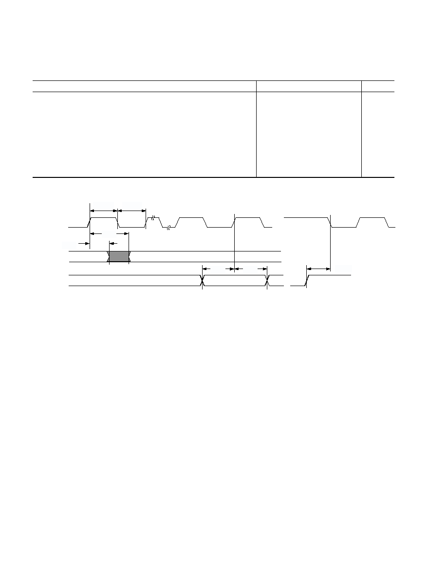
ADSP-21161N
42
REV. A
Table 28. Link Ports
Transmit
Parameter
Min
Max
Unit
Timing Requirements
t
SLACH
LACK Setup Before LCLK High
8
ns
t
HLACH
LACK Hold After LCLK High
2
ns
Switching Characteristics
t
DLDCH
Data Delay After LCLK High
3
ns
t
HLDCH
Data Hold After LCLK High
0
ns
t
LCLKTWL
LCLK Width Low
0.5t
LCLK
1.0
0.5t
LCLK
+1.0
ns
t
LCLKTWH
LCLK Width High
0.5t
LCLK
1.0
0.5t
LCLK
+1.0
ns
t
DLACLK
LCLK Low Delay After LACK High
0.5t
LCLK
+3
3t
LCLK
+11
ns
Figure 31. Link Ports--Transmit
LCLK
LDAT7-0
LACK (IN)
THE
t
SLACH
REQUIREMENT APPLIES TO THE RISING EDGE OF LCLK ONLY FOR THE FIRST NIBBLE TRANSMITTED.
TRANSMIT
LAST NIBBLE/BYTE
TRANSMITTED
FIRST NIBBLE/BYTE
TRANSMITTED
LCLK INACTIVE
(HIGH)
OUT
t
DLDCH
t
HLDCH
t
LCLKTWH
t
LCLKTWL
t
SLACH
t
HLACH
t
DLACLK

43
REV. A
ADSP-21161N
Serial Ports
To determine whether communication is possible between two
devices at clock speed n, the following specifications must be
confirmed: 1) frame sync delay and frame sync setup and hold,
2) data delay and data setup and hold, and 3) SCLK width.
Table 29. Serial Ports
External Clock
Parameter
Min
Max
Unit
Timing Requirements
t
SFSE
Transmit/Receive FS Setup Before Transmit/Receive
SCLK
1
3.5
ns
t
HFSE
Transmit/Receive FS Hold After Transmit/Receive
SCLK
1
4
ns
t
SDRE
Receive Data Setup Before Receive SCLK
1
1.5
ns
t
HDRE
Receive Data Hold After Receive SCLK
1
4
ns
t
SCLKW
SCLKx Width
7
ns
t
SCLK
SCLKx Period
2t
CCLK
ns
1
Referenced to sample edge.
Table 30. Serial Ports
Internal Clock
Parameter
Min
Max
Unit
Timing Requirements
t
SFSI
FS Setup Time Before SCLK (Transmit/Receive Mode)
1
8
ns
t
HFSI
FS Hold After SCLK (Transmit/Receive Mode)
1
0.5t
CCLK
+1
ns
t
SDRI
Receive Data Setup Before SCLK
1
4
ns
t
HDRI
Receive Data Hold After SCLK
1
3
ns
1
Referenced to sample edge.
Table 31. Serial Ports
External Clock
Parameter
Min
Max
Unit
Switching Characteristics
t
DFSE
FS Delay After SCLK (Internally Generated FS)
1, 2, 3
13
ns
t
HOFSE
FS Hold After SCLK (Internally Generated FS)
1, 2 , 3
3
ns
t
DDTE
Transmit Data Delay After SCLK
1, 2
16
ns
t
HDTE
Transmit Data Hold After SCLK
1, 2
0
ns
1
Referenced to drive edge.
2
SCLK/FS Configured as a transmit clock/frame sync with the DDIR bit = 1 in SPCTLx register.
3
SCLK/FS Configured as a receive clock/frame sync with the DDIR bit = 0 in SPCTLx register.
Table 32. Serial Ports
Internal Clock
Parameter
Min
Max
Unit
Switching Characteristics
t
DFSI
FS Delay After SCLK (Internally Generated FS)
1, 2, 3
4.5
ns
t
HOFSI
FS Hold After SCLK (Internally Generated FS)
1, 2, 3
1.5
ns
t
DDTI
Transmit Data Delay After SCLK
1, 2
7.5
ns
t
HDTI
Transmit Data Hold After SCLK
1, 2
0
ns
t
SCLKIW
SCLK Width
2
0.5t
SCLK
2.5
0.5t
SCLK
+2
ns
1
Referenced to drive edge.
2
SCLK/FS Configured as a transmit clock/frame sync with the DDIR bit = 1 in SPCTLx register.
3
SCLK/FS Configured as a receive clock/frame sync with the DDIR bit = 0 in SPCTLx register.

ADSP-21161N
44
REV. A
Table 33. Serial Ports
Enable and Three-State
Parameter
Min
Max
Unit
Switching Characteristics
t
DDTEN
Data Enable from External Transmit SCLK
1, 2
4
ns
t
DDTTE
Data Disable from External Transmit SCLK
1
10
ns
t
DDTIN
Data Enable from Internal Transmit SCLK
1
0
ns
t
DDTTI
Data Disable from Internal Transmit SCLK
1
3
ns
1
Referenced to drive edge.
2
SCLK/FS Configured as a transmit clock/frame sync with the DDIR bit = 1 in SPCTLx register.
Table 34. Serial Ports
External Late Frame Sync
Parameter
Min
Max
Unit
Switching Characteristics
t
DDTLFSE
Data Delay from Late External Transmit FS or External
Receive FS with MCE = 1, MFD = 0
1
13
ns
t
DDTENFS
Data Enable from Late FS or MCE = 1, MFD = 0
1
0.5
ns
1
MCE = 1, Transmit FS enable and Transmit FS valid follow t
DDTLFSE
and t
DDTENFS
.
45
REV. A
ADSP-21161N
Figure 32. Serial Ports
DRIVE EDGE
SCLK (INT)
DRIVE EDGE
SCLK
DRIVE EDGE
DRIVE EDGE
SCLK
SCLK (EXT)
t
DDTTE
t
DDTEN
t
DDTTI
t
DDTIN
D
X
A/D
X
B
D
X
A/D
X
B
SCLK
FS
DRIVE EDGE
SAMPLE EDGE
DATA RECEIVE-- INTERNAL CLOCK
DATA RECEIVE-- EXTERNAL CLOCK
SCLK
FS
DRIVE EDGE
SAMPLE EDGE
NOTE: EITHER THE RISING EDGE OR FALLING EDGE OF SCLK (EXTERNAL), SCLK (INTERNAL) CAN BE USED AS THE ACTIVE SAMPLING EDGE.
t
SDRI
t
HDRI
t
SFSI
t
HFSI
t
DFSI
t
HOFSI
t
SCLKIW
t
SDRE
t
HDRE
t
SFSE
t
HFSE
t
DFSE
t
SCLKW
t
HOFSE
D
X
A/D
X
B
D
X
A/D
X
B
t
DDTI
SCLK
FS
DRIVE EDGE
SAMPLE EDGE
DATA TRANSMIT -- INTERNAL CLOCK
t
SFSI
t
HFSI
t
DFSI
t
HOFSI
t
SCLKIW
D
X
A/D
X
B
t
HDTI
NOTE: EITHER THE RISING EDGE OR FALLING EDGE OF SCLK (EXTERNAL), SCLK (INTERNAL) CAN BE USED AS THE ACTIVE SAMPLING EDGE.
t
DDTE
SCLK
FS
DRIVE EDGE
SAMPLE EDGE
DATA TRANSMIT -- EXTERNAL CLOCK
t
SFSE
t
HFSE
t
DFSE
t
HOFSE
t
SCLKW
D
X
A/D
X
B
t
HDTE
ADSP-21161N
46
REV. A
Figure 33. Serial Ports
External Late Frame Sync
DRIVE
SAMPLE
DRIVE
SCLK
FS
D
X
A/D
X
B
DRIVE
SAMPLE
DRIVE
LATE EXTERNAL TRANSMIT FS
EXTERNAL RECEIVE FS WITH MCE = 1, MFD = 0
1ST BIT
2ND BIT
SCLK
FS
1ST BIT
2ND BIT
t
HOFSE/I
t
SFSE/I
t
DDTE/I
t
DDTENFS
t
DDTLFSE
t
HDTE/I
t
HOFSE/I
t
SFSE/I
t
DDTE/I
t
DDTENFS
t
DDTLFSE
t
HDTE/I
D
X
A/D
X
B
47
REV. A
ADSP-21161N
SPI Interface Specifications
Table 35. SPI Interface Protocol
Master Switching and Timing
Parameter
Min
Max
Unit
Timing Requirements
t
SSPIDM
Data Input Valid to SPICLK Edge (Data Input Set-up
Time)
0.5t
CCLK
+10
ns
t
HSPIDM
SPICLK Last Sampling Edge to Data Input Not Valid
0.5t
CCLK
+1
ns
t
SPITDM
Sequential Transfer Delay
2t
CCLK
ns
Switching Characteristics
t
SPICLKM
Serial Clock Cycle
8 t
CCLK
ns
t
SPICHM
Serial Clock High Period
4t
CCLK
4
ns
t
SPICLM
Serial Clock Low Period
4t
CCLK
4
ns
t
DDSPIDM
SPICLK Edge to Data Out Valid (Data Out Delay Time)
3
ns
t
HDSPIDM
SPICLK Edge to Data Out Not Valid (Data Out Hold Time)
0
ns
t
SDSCIM_0
FLAG30 (SPI Device Select) Low to First SPICLK Edge
for CPHASE = 0
5t
CCLK
ns
t
SDSCIM_1
FLAG30 (SPI Device Select) Low to First SPICLK Edge
for CPHASE = 1
3t
CCLK
ns
t
HDSM
Last SPICLK Edge to FLAG30 High
t
CCLK
3
ns
Table 36. SPI Interface Protocol
Slave Switching and Timing
Parameter
Min
Max
Unit
Timing Requirements
t
SPICLKS
Serial Clock Cycle
8t
CCLK
ns
t
SPICHS
Serial Clock High Period
4t
CCLK
4
ns
t
SPICLS
Serial Clock Low Period
4t
CCLK
4
ns
t
SDSCO
SPIDS Assertion to First SPICLK Edge
CPHASE = 0
3.5t
CCLK
+8
ns
CPHASE = 1
1.5t
CCLK
+8
ns
t
HDS
Last SPICLK Edge to
SPIDS Not Asserted
CPHASE = 0
0
ns
t
SSPIDS
Data Input Valid to SPICLK Edge (Data Input Set-up Time) 0
ns
t
HSPIDS
SPICLK Last Sampling Edge to Data Input Not Valid
t
CCLK
+1
ns
t
SDPPW
SPIDS Deassertion Pulsewidth (CPHASE = 0)
t
CCLK
ns
Switching Characteristics
t
DSOE
SPIDS Assertion to Data Out Active
2
0.5t
CCLK
+5.5
ns
t
DSDHI
SPIDS Deassertion to Data High Impedance
1.5
0.5t
CCLK
+5.5
ns
t
DDSPIDS
SPICLK Edge to Data Out Valid (Data Out Delay Time)
0.75t
CCLK
+3
ns
t
HDSPIDS
1
SPICLK Edge to Data Out Not Valid (Data Out Hold Time) 0.25t
CCLK
+3
ns
t
HDLSBS
1
SPICLK Edge to Last Bit Out Not Valid
(Data Out Hold Time) for LSB
0.5t
SPICLK
+4.5t
CCLK
ns
t
DSOV
2
SPIDS Assertion to Data Out Valid (CPHASE = 0)
1.5t
CCLK
+7
ns
1
When CPHASE = 0 and baud rate is greater than 1, t
HDLSBS
affects the length of the last bit transmitted.
2
Applies to the first deassertion of
SPIDS only.
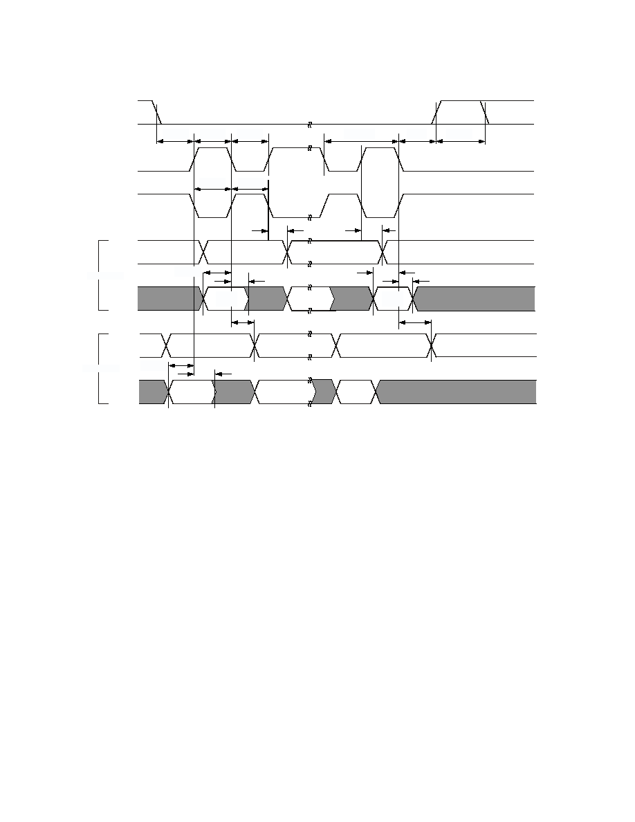
ADSP-21161N
48
REV. A
Figure 34. SPI Interface Protocol
Master Switching and Timing
t
S S P ID M
t
H S P I D M
t
H D S P I D M
LS B
MS B
t
H S S P I D M
t
D D S P ID M
MO S I
(O UTP UT)
MI SO
(INP UT)
FL AG3- 0
(O UTP UT )
S PICLK
(C P = 0)
(O UTP UT )
S PIC LK
(CP = 1)
(O UTP UT )
t
S P I C H M
t
S P I C L M
t
S P I C L M
t
S P I C L K M
t
S P I C H M
t
H D S M
t
S P I T D M
t
H D SP I D M
L SB
V ALID
L S B
MS B
MS B
VAL ID
t
H S P I D M
t
D D S P I D M
MO S I
(O UTP UT)
MI SO
(INP UT)
t
S S P I D M
CPHASE = 1
CPHASE = 0
MS B
V ALID
t
S D S C I M
t
S S P ID M
L SB
VA LID
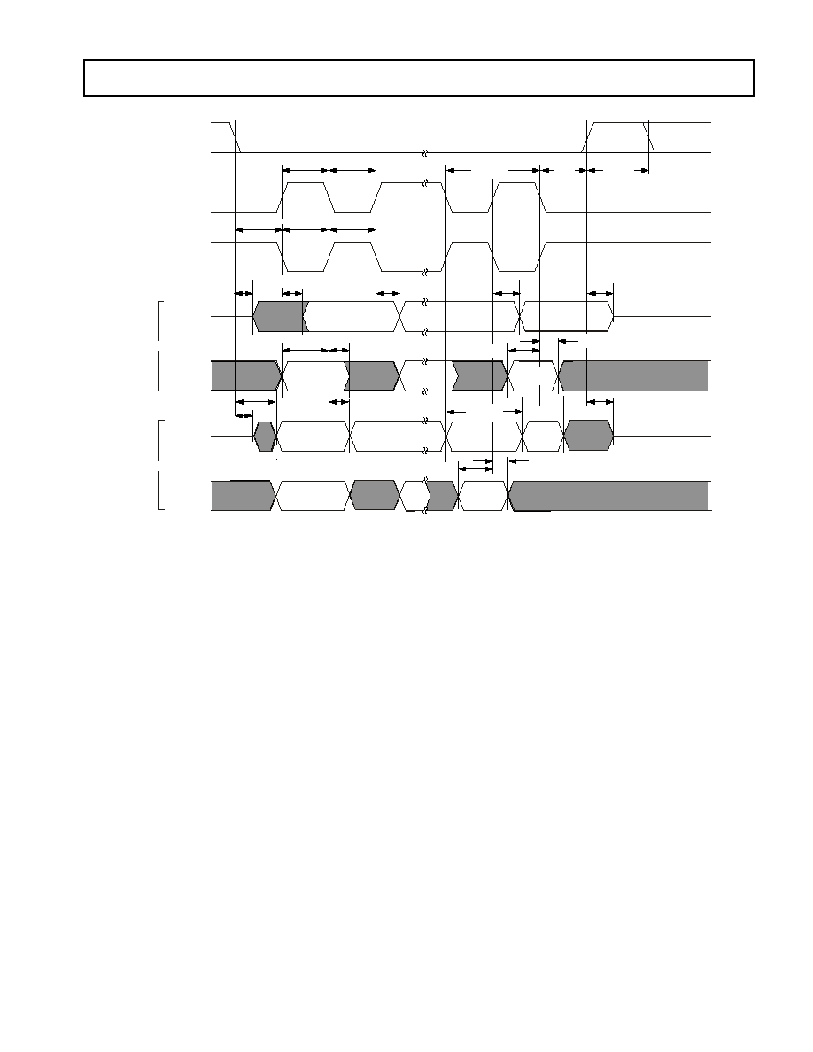
49
REV. A
ADSP-21161N
Figure 35. SPI Interface Protocol
Slave Switching and Timing
t
H S P ID S
t
D D S P I D S
t
D S D H I
L SB
MSB
MSB
VA LID
t
H S P I D S
t
D S O E
t
D D S P I D S
t
H D S P I D S
MISO
(OUTPUT )
MOSI
(IN PUT)
t
S S P I D S
SPIDS
(INPUT)
SPICLK
( CP = 0)
( INPUT)
SPICLK
( CP = 1)
( INPUT)
t
S D S C O
t
S P I C H S
t
S P I C L S
t
S P IC LS
t
S P I C L K S
t
H D S
t
S P I C H S
t
S SP I D S
t
H S P I D S
t
D S D H I
L SB
VA LID
MSB
MSB VALI D
t
D S O E
t
D D S P ID S
MISO
(OUTPUT )
MOSI
(IN PUT)
t
S S P I D S
L SB
VA LID
LSB
CPH ASE = 1
CPH ASE = 0
t
S D P P W
t
D S O V
t
H D L S B S
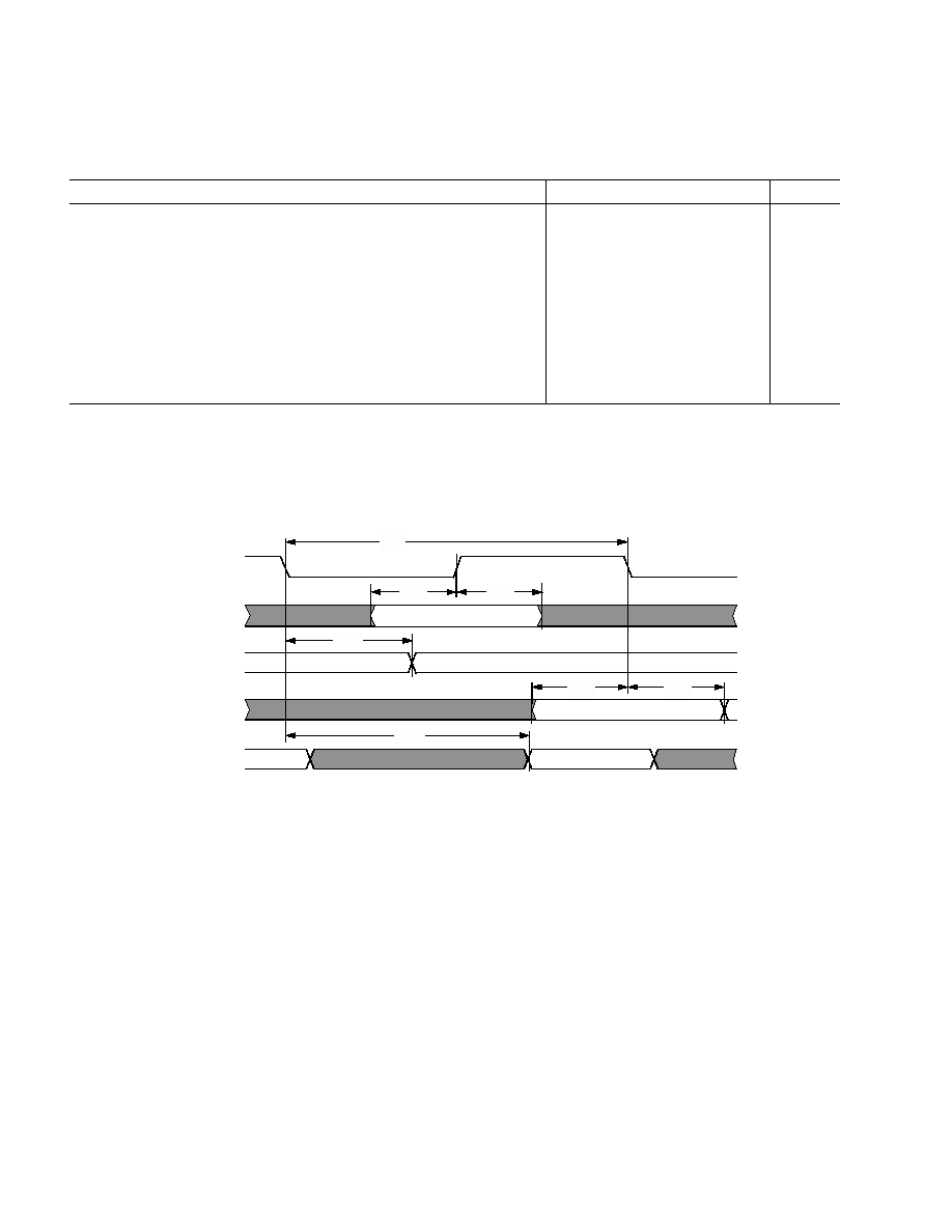
ADSP-21161N
50
REV. A
JTAG Test Access Port and Emulation
Table 37. JTAG Test Access Port and Emulation
Parameter
Min
Max Unit
Timing Requirements
t
TCK
TCK Period
t
CK
ns
t
STAP
TDI, TMS Setup Before TCK High
5
ns
t
HTAP
TDI, TMS Hold After TCK High
6
ns
t
SSYS
System Inputs Setup Before TCK Low
1
2
ns
t
HSYS
System Inputs Hold After TCK Low
1
15
ns
t
TRSTW
TRST Pulsewidth
4t
CK
ns
Switching Characteristics
t
DTDO
TDO Delay from TCK Low
13
ns
t
DSYS
System Outputs Delay After TCK Low
2
30
ns
1
System Inputs = DATA4716, ADDR230,
RD, WR, ACK, RPBA, SPIDS, EBOOT, LBOOT, DMAR21, CLK_CFG10, CLKDBL, CS, HBR,
SBTS, ID20, IRQ20, RESET, BMS, MISO, MOSI, SPICLK, DxA, DxB, SCLKx, FSx, LxDAT70, LxCLK, LxACK, SDWE, HBG, RAS, CAS,
SDCLK0, SDCKE, BRST,
BR61, PA, MS30, FLAG110.
2
System Outputs =
BMS, MISO, MOSI, SPICLK, DxA, DxB, SCLKx, FSx, LxDAT70, LxCLK, LxACK, DATA4716, SDWE, ACK, HBG, RAS,
CAS, SDCLK10, SDCKE, BRST, RD, WR, BR61, PA, MS30, ADDR230, FLAG110, DMAG21, DQM, REDY, CLKOUT, SDA10,
TIMEXP,
EMU, BMSTR, RSTOUT.
Figure 36. JTAG Test Access Port and Emulation
TCK
TMS
TDI
TDO
SYSTEM
INPUTS
SYSTEM
OUTPUTS
t
STAP
t
TCK
t
HTAP
t
DTDO
t
SSYS
t
HSYS
t
DSYS
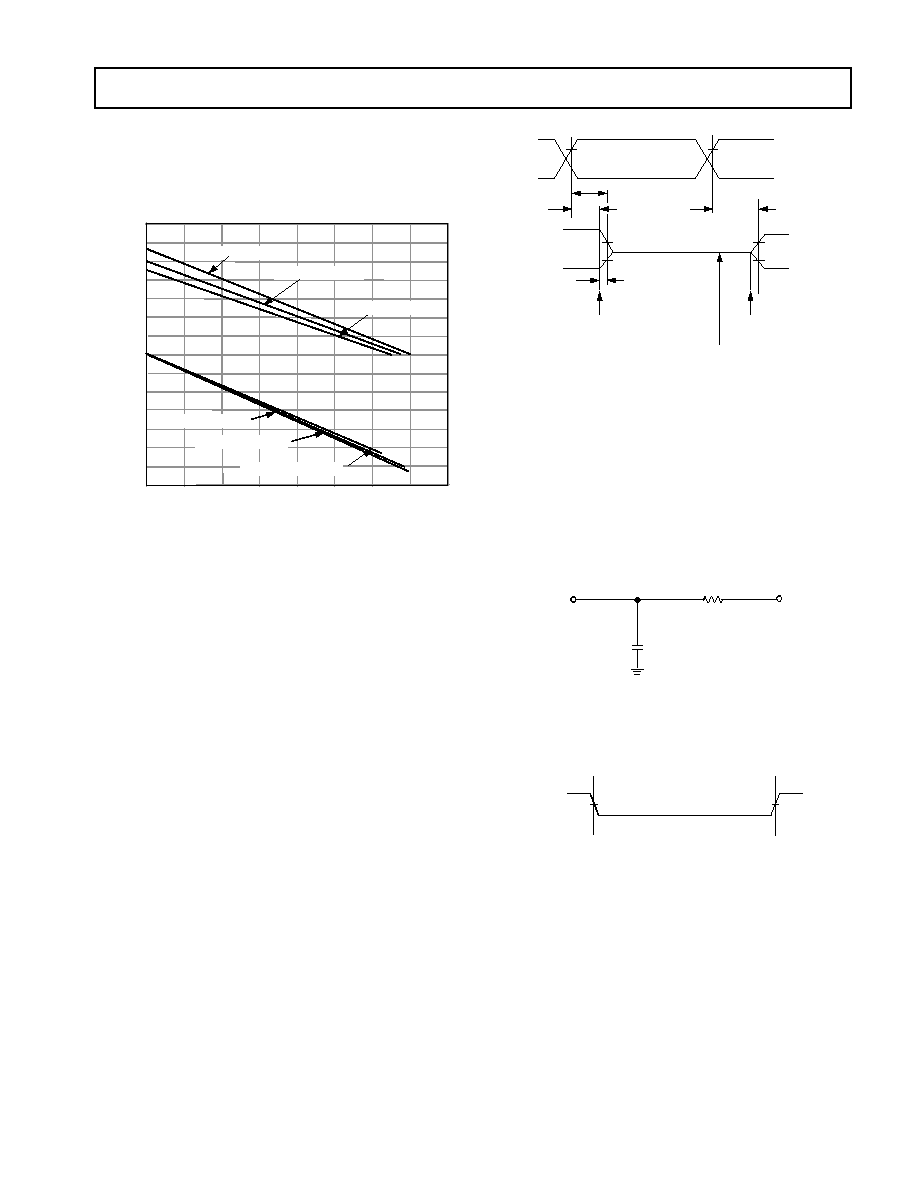
51
REV. A
ADSP-21161N
Output Drive Currents
Figure 37
shows typical I-V characteristics for the output drivers
of the ADSP-21161N. The curves represent the current drive
capability of the output drivers as a function of output voltage.
Test Conditions
The DSP is tested for output enable, disable, and hold time.
Output Enable Time
Output pins are considered to be enabled when they have made
a transition from a high impedance state to the point when they
start driving. The output enable time t
ENA
is the interval from the
point when a reference signal reaches a high or low voltage level
to the point when the output has reached a specified high or low
trip point, as shown in the Output Enable/Disable diagram
(
Figure 38
). If multiple pins (such as the data bus) are enabled,
the measurement value is that of the first pin to start driving.
Output Disable Time
Output pins are considered to be disabled when they stop driving,
go into a high impedance state, and start to decay from their
output high or low voltage. The time for the voltage on the bus
to decay by
V is dependent on the capacitive load, C
L
and the
load current, I
L
. This decay time can be approximated by the
following equation:
The output disable time t
DIS
is the difference between t
MEASURED
and t
DECAY
as shown in
Figure 38
. The time t
MEASURED
is the
interval from when the reference signal switches to when the
output voltage decays
V from the measured output high or
output low voltage. t
DECAY
is calculated with test loads C
L
and I
L
,
and with
V equal to 0.5 V.
Example System Hold Time Calculation
To determine the data output hold time in a particular system,
first calculate t
DECAY
using the equation given above. Choose
V
to be the difference between the ADSP-21161N's output voltage
and the input threshold for the device requiring the hold time. A
typical
V will be 0.4 V. C
L
is the total bus capacitance (per data
line), and I
L
is the total leakage or three-state current (per data
line). The hold time will be t
DECAY
plus the minimum disable time
(i.e., t
DATRWH
for the write cycle).
Figure 37. Typical Drive Currents
SWEEP (V
DDEXT
) VOLTAGE V
60
10
40
0
3.5
0.5
1.0
1.5
2.0
2.5
3.0
50
0
20
30
30
10
40
20
50
60
L
O
A
D
(
V
D
D
E
X
T
)
C
U
R
R
E
N
T
m
A
V
DDEXT
= 3.47V, 40°C
V
DDEXT
= 3.3V, +25°C
V
DDEXT
= 3.13V, +105°C
V
DDEXT
= 3.13V, +105°C
V
DDEXT
= 3.47V, 40°C
V
DDEXT
= 3.3V, +25°C
80
80
t
DECAY
C
L
V
(
)
I
L
---------------------
=
Figure 38. Output Enable/Disable
Figure 39. 31Equivalent Device Loading for AC
Measurements (Includes All Fixtures)
Figure 40. Voltage Reference Levels for AC
Measurements (Except Output Enable/Disable)
REFERENCE
SIGNAL
t
DIS
OUTPUT STARTS DRIVING
V
OH
(MEASURED)
V
V
OL
(MEASURED) +
V
t
MEASURED
V
OH
(MEASURED)
V
OL
(MEASURED)
2.0V
1.0V
V
OH
(MEASURED)
V
OL
(MEASURED)
HIGH IMPEDANCE STATE.
TEST CONDITIONS CAUSE THIS
VOLTAGE TO BE APPROXIMATELY 1.5V.
OUTPUT STOPS DRIVING
t
ENA
t
DECAY
1.5V
30pF
TO
OUTPUT
PIN
50
INPUT
OR
OUTPUT
1.5V
1.5V
ADSP-21161N
52
REV. A
Capacitive Loading
Output delays and holds are based on standard capacitive loads:
30 pF on all pins (see
Figure 39 on Page 51
).
Figure 41
shows
graphically how output delays and holds vary with load capaci-
tance. (Note that this graph or derating does not apply to output
disable delays; see
Output Disable Time on Page 51
.) The graphs
of
Figure 41
,
Figure 42
, and
Figure 43
may not be linear outside
the ranges shown for Typical Output Delay vs. Load Capacitance
and Typical Output Rise Time (20% 80%, V = Min) vs. Load
Capacitance.
Environmental Conditions
The thermal characteristics in which the DSP is operating
influence performance.
Thermal Characteristics
The ADSP-21161N is packaged in a 225-ball Mini Ball Grid
Array (MBGA). The ADSP-21161N is specified for a case tem-
perature (T
CASE
). To ensure that the T
CASE
data sheet specification
is not exceeded, a heatsink and/or an air flow source may be used.
Use the center block of ground pins (MBGA balls: F6-10,
G6-10, H6-10, J6-10, K6-10) to provide thermal pathways to the
printed circuit board's ground plane. A heatsink should be
attached to the ground plane (as close as possible to the thermal
pathways) with a thermal adhesive.
where:
·
T
CASE
= Case temperature (measured on top surface
of package)
·
PD = Power dissipation in W (this value depends upon
the specific application; a method for calculating PD is
shown under Power Dissipation).
·
CA
= Value from
Table 38
.
·
JB
= 8.0°C/W
Figure 41. Typical Output Delay or Hold vs. Load
Capacitance (at Max Case Temperature)
Figure 42. Typical Output Rise/Fall Time (20% 80%,
V
DDEXT
= Max)
Figure 43. Typical Output Rise/Fall Time (20% 80%,
V
DDEXT
= Min)
LOAD CAPACITANCE pF
25
5
0
210
30
60
90
120
150
180
20
15
10
5
NOMINAL
Y = 0.0835X - 2.42
O
U
T
P
U
T
D
E
L
A
Y
O
R
H
O
L
D
n
s
LOAD CAPACITANCE pF
16.0
8.0
0
0
200
20
40
60
80
100
120
140
160
180
14.0
12.0
4.0
2.0
10.0
6.0
FALL TIME
RISE TIME
Y = 0.0743X + 1.5613
R
I
S
E
A
N
D
F
A
L
L
T
I
M
E
S
n
s
(
0
.
6
9
4
V
T
O
2
.
7
7
V
,
2
0
%
T
O
8
0
%
)
Y = 0.0414X + 2.0128
LOAD CAPACITANCE pF
16.0
8.0
0
0
200
20
40
60
80
100
120
140
160
180
14.0
12.0
4.0
2.0
10.0
6.0
FALL TIME
RISE TIME
Y = 0.0773X + 1.4399
R
I
S
E
A
N
D
F
A
L
L
T
I
M
E
S
n
s
(
0
.
6
9
4
V
T
O
2
.
7
7
V
,
2
0
%
T
O
8
0
%
)
Y = 0.0417X + 1.8674
Table 38. Airflow Over Package Versus
CA
Airflow (Linear Ft./Min.)
0
200
400
CA
(°C/W)
1
1
JC
= 6.8°C/W.
17.9
15.2
13.7
T
CASE
T
AMB
PD
CA
×
(
)
+
=

53
REV. A
ADSP-21161N
225-BALL METRIC MBGA PIN CONFIGURATIONS
Table 39. 225-Ball Metric MBGA Pin Assignments
Pin Name
PBGA
Pin Number
Pin Name
PBGA
Pin Number
Pin Name
PBGA
Pin Number
Pin Name
PBGA
Pin Number
NC
A01
TRST
B01
TMS
C01
TDO
D01
BMSTR
A02
TDI
B02
EMU
C02
TCK
D02
BMS
A03
RPBA
B03
GND
C03
FLAG11
D03
SPIDS
A04
MOSI
B04
SPICLK
C04
MISO
D04
EBOOT
A05
FS0
B05
D0B
C05
SCLK0
D05
LBOOT
A06
SCLK1
B06
D1A
C06
D1B
D06
SCLK2
A07
D2B
B07
D2A
C07
FS1
D07
D3B
A08
D3A
B08
FS2
C08
V
DDINT
D08
L0DAT4
A09
L0DAT7
B09
FS3
C09
SCLK3
D09
L0ACK
A10
L0CLK
B10
L0DAT6
C10
L0DAT5
D10
L0DAT2
A11
L0DAT1
B11
L1DAT7
C11
L0DAT3
D11
L1DAT6
A12
L1DAT4
B12
L1DAT3
C12
L1DAT5
D12
L1CLK
A13
L1ACK
B13
L1DAT1
C13
DATA42
D13
L1DAT2
A14
L1DAT0
B14
DATA45
C14
DATA46
D14
NC
A15
RSTOUT
1
B15
DATA47
C15
DATA44
D15
FLAG10
E01
FLAG5
F01
FLAG1
G01
FLAG0
H01
RESET
E02
FLAG7
F02
FLAG2
G02
IRQ0
H02
FLAG8
E03
FLAG9
F03
FLAG4
G03
V
DDINT
H03
D0A
E04
FLAG6
F04
FLAG3
G04
IRQ1
H04
V
DDEXT
E05
V
DDINT
F05
V
DDEXT
G05
V
DDINT
H05
V
DDINT
E06
GND
F06
GND
G06
GND
H06
V
DDEXT
E07
GND
F07
GND
G07
GND
H07
V
DDINT
E08
GND
F08
GND
G08
GND
H08
V
DDEXT
E09
GND
F09
GND
G09
GND
H09
V
DDINT
E10
GND
F10
GND
G10
GND
H10
V
DDEXT
E11
V
DDINT
F11
V
DDEXT
G11
V
DDINT
H11
L0DAT0
E12
DATA37
F12
DATA34
G12
DATA29
H12
DATA39
E13
DATA40
F13
DATA35
G13
DATA28
H13
DATA43
E14
DATA38
F14
DATA33
G14
DATA30
H14
DATA41
E15
DATA36
F15
DATA32
G15
DATA31
H15
IRQ2
J01
TIMEXP
K01
ADDR19
L01
ADDR16
M01
ID1
J02
ADDR22
K02
ADDR17
L02
ADDR12
M02
ID2
J03
ADDR20
K03
ADDR21
L03
ADDR18
M03
ID0
J04
ADDR23
K04
ADDR2
L04
ADDR6
M04
V
DDEXT
J05
V
DDINT
K05
V
DDEXT
L05
ADDR0
M05
GND
J06
GND
K06
V
DDINT
L06
MS1
M06
GND
J07
GND
K07
V
DDEXT
L07
BR6
M07
GND
J08
GND
K08
V
DDINT
L08
V
DDEXT
M08
GND
J09
GND
K09
V
DDEXT
L09
WR
M09
GND
J10
GND
K10
V
DDINT
L10
SDA10
M10
V
DDEXT
J11
V
DDINT
K11
V
DDEXT
L11
RAS
M11
DATA26
J12
DATA22
K12
CAS
L12
ACK
M12
DATA24
J13
DATA19
K13
DATA20
L13
DATA17
M13
DATA25
J14
DATA21
K14
DATA16
L14
DMAG2
M14
DATA27
J15
DATA23
K15
DATA18
L15
DMAG1
M15
ADSP-21161N
54
REV. A
ADDR14
N01
ADDR13
P01
NC
R01
ADDR15
N02
ADDR9
P02
ADDR11
R02
ADDR10
N03
ADDR8
P03
ADDR7
R03
ADDR5
N04
ADDR4
P04
ADDR3
R04
ADDR1
N05
MS2
P05
MS3
R05
MS0
N06
SBTS
P06
PA
R06
BR5
N07
BR4
P07
BR3
R07
BR2
N08
BR1
P08
RD
R08
BRST
N09
SDCLK1
P09
CLKOUT
R09
SDCKE
N10
SDCLK0
P10
HBR
R10
CS
N11
REDY
P11
HBG
R11
CLK_CFG1
N12
CLKIN
P12
CLKDBL
R12
CLK_CFG0
N13
DQM
P13
XTAL
R13
AVDD
N14
AGND
P14
SDWE
R14
DMAR1
N15
DMAR2
P15
NC
R15
1
RSTOUT exists only for silicon revisions 1.2 and greater. Leave this pin unconnected for silicon revisions 0.3, 1.0, and 1.1.
Figure 44. 225-Ball Metric MBGA Pin Assignments (Bottom View, Summary)
Table 39. 225-Ball Metric MBGA Pin Assignments (continued)
Pin Name
PBGA
Pin Number
Pin Name
PBGA
Pin Number
Pin Name
PBGA
Pin Number
Pin Name
PBGA
Pin Number
VDDINT
VDDEXT
GND
*
AGND
AVDD
SIGNAL
*
USE THE CENTER BLOCK OF GROUND PINS TO PROVIDE THERMAL
PATHWAYS TO YOUR PRINTED CIRCUIT BOARD GROUND PLANE
KEY:
1
2
3
4
5
6
7
8
9
10
11
12
14
15
13
R
P
N
M
L
K
J
H
G
F
E
D
C
B
A
55
REV. A
ADSP-21161N
OUTLINE DIMENSIONS
The ADSP-21161N comes in a 17 mm
×
17 mm, 225-ball MBGA package with 15 rows of balls.
ORDERING GUIDE
225-Ball Mini-BGA (CA-225)
Part Number
1
1
These parts are packaged in a 225-ball Mini-Ball Grid Array (MBGA).
Case Temperature
Range
Instruction Rate
On-Chip
SRAM
Operating Voltage
ADSP-21161NKCA-100
0
°
C to +85
°
C
100 MHz
1 M bit
1.8 int/3.3 ext V
ADSP-21161NCCA-100
40
°
C to +105
°
C
100 MHz
1 M bit
1.8 int/3.3 ext V
1.85 MAX
(SEE NOTE 1)
DETAIL A
1.00
BSC
A
B
C
D
E
F
G
H
J
K
L
M
N
P
R
15 14 13 12 11 10 9 8 7 6 5 4 3 2 1
SEATING
PLANE
1.31 MAX
(SEE NOTE 1)
0.20 MAX
0.70
0.60
0.50
(BALL DIAMETER)
0.30 MIN
DETAIL A
TOP VIEW
BOTTOM VIEW
A1 BALL
INDICATOR
14.00
BSC
SQ
17.00
BSC
1.00 BSC (BALL PITCH)
17.00
BSC
NOTES:
1. DIMENSIONS ARE IN MILLIMETERS AND COMPLY WITH JEDEC STANDARD MO-192-AAF2, EXCEPT FOR HEIGHT
AND THICKNESS DIMENSIONS NOTED.
2. ACTUAL POSITION OF THE BALL GRID IS WITHIN 0.25 OF ITS IDEAL POSITION RELATIVE TO THE PACKAGE EDGES.
3. ACTUAL POSITION OF EACH BALL IS WITHIN 0.10 OF ITS IDEAL POSITION RELATIVE TO THE BALL GRID.

ADSP-21161N
56
REV. A
Revision History
Location
Page
5/03--Changed from Rev. 0 to Rev. A
Changes to:
KEY FEATURES . . . . . . . . . . . . . . . . . . . . . . . . . . . . . . . . . . . . . . . . . . . . . . . . . . . . . . . . . . . . . . . . . . . . . . . . . .
2
Table 1 . . . . . . . . . . . . . . . . . . . . . . . . . . . . . . . . . . . . . . . . . . . . . . . . . . . . . . . . . . . . . . . . . . . . . . . . . . . . . . . . . . .
3
SIMD Computational Engine . . . . . . . . . . . . . . . . . . . . . . . . . . . . . . . . . . . . . . . . . . . . . . . . . . . . . . . . . . . . . . . . . .
5
Figure 2 . . . . . . . . . . . . . . . . . . . . . . . . . . . . . . . . . . . . . . . . . . . . . . . . . . . . . . . . . . . . . . . . . . . . . . . . . . . . . . . . . .
6
Off-Chip Memory and Peripherals Interface . . . . . . . . . . . . . . . . . . . . . . . . . . . . . . . . . . . . . . . . . . . . . . . . . . . . . . . .
6
DMA Controller . . . . . . . . . . . . . . . . . . . . . . . . . . . . . . . . . . . . . . . . . . . . . . . . . . . . . . . . . . . . . . . . . . . . . . . . . . .
7
Host Processor Interface . . . . . . . . . . . . . . . . . . . . . . . . . . . . . . . . . . . . . . . . . . . . . . . . . . . . . . . . . . . . . . . . . . . . . .
9
Phase-Locked Loop and Crystal Double Enable . . . . . . . . . . . . . . . . . . . . . . . . . . . . . . . . . . . . . . . . . . . . . . . . . . . .
9
Design-for-Emulation Circuit Information . . . . . . . . . . . . . . . . . . . . . . . . . . . . . . . . . . . . . . . . . . . . . . . . . . . . . . .
11
Table 2 . . . . . . . . . . . . . . . . . . . . . . . . . . . . . . . . . . . . . . . . . . . . . . . . . . . . . . . . . . . . . . . . . . . . . . . . . . . . . . . . . .
12
Table 3 . . . . . . . . . . . . . . . . . . . . . . . . . . . . . . . . . . . . . . . . . . . . . . . . . . . . . . . . . . . . . . . . . . . . . . . . . . . . . . . . . .
17
ELECTRICAL CHARACTERISTICS . . . . . . . . . . . . . . . . . . . . . . . . . . . . . . . . . . . . . . . . . . . . . . . . . . . . . . . . .
18
TIMING SPECIFICATIONS . . . . . . . . . . . . . . . . . . . . . . . . . . . . . . . . . . . . . . . . . . . . . . . . . . . . . . . . . . . . . . . .
20
Table 5 . . . . . . . . . . . . . . . . . . . . . . . . . . . . . . . . . . . . . . . . . . . . . . . . . . . . . . . . . . . . . . . . . . . . . . . . . . . . . . . . . .
20
Figure 10 . . . . . . . . . . . . . . . . . . . . . . . . . . . . . . . . . . . . . . . . . . . . . . . . . . . . . . . . . . . . . . . . . . . . . . . . . . . . . . . .
20
Power Dissipation . . . . . . . . . . . . . . . . . . . . . . . . . . . . . . . . . . . . . . . . . . . . . . . . . . . . . . . . . . . . . . . . . . . . . . . . . .
21
Table 8 . . . . . . . . . . . . . . . . . . . . . . . . . . . . . . . . . . . . . . . . . . . . . . . . . . . . . . . . . . . . . . . . . . . . . . . . . . . . . . . . . .
22
Figure 11 . . . . . . . . . . . . . . . . . . . . . . . . . . . . . . . . . . . . . . . . . . . . . . . . . . . . . . . . . . . . . . . . . . . . . . . . . . . . . . . .
22
Table 9 . . . . . . . . . . . . . . . . . . . . . . . . . . . . . . . . . . . . . . . . . . . . . . . . . . . . . . . . . . . . . . . . . . . . . . . . . . . . . . . . . .
23
Figure 12 . . . . . . . . . . . . . . . . . . . . . . . . . . . . . . . . . . . . . . . . . . . . . . . . . . . . . . . . . . . . . . . . . . . . . . . . . . . . . . . .
23
Clock Input . . . . . . . . . . . . . . . . . . . . . . . . . . . . . . . . . . . . . . . . . . . . . . . . . . . . . . . . . . . . . . . . . . . . . . . . . . . . . .
24
Table 10 . . . . . . . . . . . . . . . . . . . . . . . . . . . . . . . . . . . . . . . . . . . . . . . . . . . . . . . . . . . . . . . . . . . . . . . . . . . . . . . . .
24
Figure 14 . . . . . . . . . . . . . . . . . . . . . . . . . . . . . . . . . . . . . . . . . . . . . . . . . . . . . . . . . . . . . . . . . . . . . . . . . . . . . . . .
24
Table 12 . . . . . . . . . . . . . . . . . . . . . . . . . . . . . . . . . . . . . . . . . . . . . . . . . . . . . . . . . . . . . . . . . . . . . . . . . . . . . . . . .
25
Figure 17 . . . . . . . . . . . . . . . . . . . . . . . . . . . . . . . . . . . . . . . . . . . . . . . . . . . . . . . . . . . . . . . . . . . . . . . . . . . . . . . .
25
Table 13 . . . . . . . . . . . . . . . . . . . . . . . . . . . . . . . . . . . . . . . . . . . . . . . . . . . . . . . . . . . . . . . . . . . . . . . . . . . . . . . . .
26
Figure 18 . . . . . . . . . . . . . . . . . . . . . . . . . . . . . . . . . . . . . . . . . . . . . . . . . . . . . . . . . . . . . . . . . . . . . . . . . . . . . . . .
26
Table 14 . . . . . . . . . . . . . . . . . . . . . . . . . . . . . . . . . . . . . . . . . . . . . . . . . . . . . . . . . . . . . . . . . . . . . . . . . . . . . . . . .
26
Figure 19 . . . . . . . . . . . . . . . . . . . . . . . . . . . . . . . . . . . . . . . . . . . . . . . . . . . . . . . . . . . . . . . . . . . . . . . . . . . . . . . .
26
Memory Read
Bus Master . . . . . . . . . . . . . . . . . . . . . . . . . . . . . . . . . . . . . . . . . . . . . . . . . . . . . . . . . . . . . . . . . .
27
Table 15 . . . . . . . . . . . . . . . . . . . . . . . . . . . . . . . . . . . . . . . . . . . . . . . . . . . . . . . . . . . . . . . . . . . . . . . . . . . . . . . . .
27
Figure 20 . . . . . . . . . . . . . . . . . . . . . . . . . . . . . . . . . . . . . . . . . . . . . . . . . . . . . . . . . . . . . . . . . . . . . . . . . . . . . . . .
27
Memory Write
Bus Master . . . . . . . . . . . . . . . . . . . . . . . . . . . . . . . . . . . . . . . . . . . . . . . . . . . . . . . . . . . . . . . . . .
28
Table 16 . . . . . . . . . . . . . . . . . . . . . . . . . . . . . . . . . . . . . . . . . . . . . . . . . . . . . . . . . . . . . . . . . . . . . . . . . . . . . . . . .
28
Figure 21 . . . . . . . . . . . . . . . . . . . . . . . . . . . . . . . . . . . . . . . . . . . . . . . . . . . . . . . . . . . . . . . . . . . . . . . . . . . . . . . .
28
Synchronous Read/Write
Bus Master . . . . . . . . . . . . . . . . . . . . . . . . . . . . . . . . . . . . . . . . . . . . . . . . . . . . . . . . . .
29
Table 17 . . . . . . . . . . . . . . . . . . . . . . . . . . . . . . . . . . . . . . . . . . . . . . . . . . . . . . . . . . . . . . . . . . . . . . . . . . . . . . . . .
29
Figure 22 . . . . . . . . . . . . . . . . . . . . . . . . . . . . . . . . . . . . . . . . . . . . . . . . . . . . . . . . . . . . . . . . . . . . . . . . . . . . . . . .
29
Host BusRequest . . . . . . . . . . . . . . . . . . . . . . . . . . . . . . . . . . . . . . . . . . . . . . . . . . . . . . . . . . . . . . . . . . . . . . . . . .
31
Table 19 . . . . . . . . . . . . . . . . . . . . . . . . . . . . . . . . . . . . . . . . . . . . . . . . . . . . . . . . . . . . . . . . . . . . . . . . . . . . . . . . .
31
Figure 24 . . . . . . . . . . . . . . . . . . . . . . . . . . . . . . . . . . . . . . . . . . . . . . . . . . . . . . . . . . . . . . . . . . . . . . . . . . . . . . . .
31
Table 20 . . . . . . . . . . . . . . . . . . . . . . . . . . . . . . . . . . . . . . . . . . . . . . . . . . . . . . . . . . . . . . . . . . . . . . . . . . . . . . . . .
32
Figure 25 . . . . . . . . . . . . . . . . . . . . . . . . . . . . . . . . . . . . . . . . . . . . . . . . . . . . . . . . . . . . . . . . . . . . . . . . . . . . . . . .
32
Asynchronous Read/Write
Host to
ADSP-21161N
. . . . . . . . . . . . . . . . . . . . . . . . . . . . . . . . . . . . . . . . . . . . . . . .
33
Table 21 . . . . . . . . . . . . . . . . . . . . . . . . . . . . . . . . . . . . . . . . . . . . . . . . . . . . . . . . . . . . . . . . . . . . . . . . . . . . . . . . .
33
Table 22 . . . . . . . . . . . . . . . . . . . . . . . . . . . . . . . . . . . . . . . . . . . . . . . . . . . . . . . . . . . . . . . . . . . . . . . . . . . . . . . . .
33
Three-State Timing
Bus Master, Bus Slave . . . . . . . . . . . . . . . . . . . . . . . . . . . . . . . . . . . . . . . . . . . . . . . . . . . . . .
35
Figure 27 . . . . . . . . . . . . . . . . . . . . . . . . . . . . . . . . . . . . . . . . . . . . . . . . . . . . . . . . . . . . . . . . . . . . . . . . . . . . . . . .
36
Table 23 . . . . . . . . . . . . . . . . . . . . . . . . . . . . . . . . . . . . . . . . . . . . . . . . . . . . . . . . . . . . . . . . . . . . . . . . . . . . . . . . .
35
Table 24 . . . . . . . . . . . . . . . . . . . . . . . . . . . . . . . . . . . . . . . . . . . . . . . . . . . . . . . . . . . . . . . . . . . . . . . . . . . . . . . . .
37
Figure 28 . . . . . . . . . . . . . . . . . . . . . . . . . . . . . . . . . . . . . . . . . . . . . . . . . . . . . . . . . . . . . . . . . . . . . . . . . . . . . . . .
38

57
REV. A
ADSP-21161N
Changes to:
Table 25 . . . . . . . . . . . . . . . . . . . . . . . . . . . . . . . . . . . . . . . . . . . . . . . . . . . . . . . . . . . . . . . . . . . . . . . . . . . . . . . .
39
Table 26 . . . . . . . . . . . . . . . . . . . . . . . . . . . . . . . . . . . . . . . . . . . . . . . . . . . . . . . . . . . . . . . . . . . . . . . . . . . . . . . .
39
Figure 29 . . . . . . . . . . . . . . . . . . . . . . . . . . . . . . . . . . . . . . . . . . . . . . . . . . . . . . . . . . . . . . . . . . . . . . . . . . . . . . . .
40
Table 29 . . . . . . . . . . . . . . . . . . . . . . . . . . . . . . . . . . . . . . . . . . . . . . . . . . . . . . . . . . . . . . . . . . . . . . . . . . . . . . . .
43
Table 30 . . . . . . . . . . . . . . . . . . . . . . . . . . . . . . . . . . . . . . . . . . . . . . . . . . . . . . . . . . . . . . . . . . . . . . . . . . . . . . . .
43
Table 31 . . . . . . . . . . . . . . . . . . . . . . . . . . . . . . . . . . . . . . . . . . . . . . . . . . . . . . . . . . . . . . . . . . . . . . . . . . . . . . . . .
43
Table 32 . . . . . . . . . . . . . . . . . . . . . . . . . . . . . . . . . . . . . . . . . . . . . . . . . . . . . . . . . . . . . . . . . . . . . . . . . . . . . . . .
43
Table 36 . . . . . . . . . . . . . . . . . . . . . . . . . . . . . . . . . . . . . . . . . . . . . . . . . . . . . . . . . . . . . . . . . . . . . . . . . . . . . . . .
47
Figure 35 . . . . . . . . . . . . . . . . . . . . . . . . . . . . . . . . . . . . . . . . . . . . . . . . . . . . . . . . . . . . . . . . . . . . . . . . . . . . . . . .
49
Figure 37 . . . . . . . . . . . . . . . . . . . . . . . . . . . . . . . . . . . . . . . . . . . . . . . . . . . . . . . . . . . . . . . . . . . . . . . . . . . . . . . .
51
Figure 39 . . . . . . . . . . . . . . . . . . . . . . . . . . . . . . . . . . . . . . . . . . . . . . . . . . . . . . . . . . . . . . . . . . . . . . . . . . . . . . . .
51
Table 39 . . . . . . . . . . . . . . . . . . . . . . . . . . . . . . . . . . . . . . . . . . . . . . . . . . . . . . . . . . . . . . . . . . . . . . . . . . . . . . . .
53
OUTLINE DIMENSIONS . . . . . . . . . . . . . . . . . . . . . . . . . . . . . . . . . . . . . . . . . . . . . . . . . . . . . . . . . . . . . . . . . .
55
Changes to formatting . . . . . . . . . . . . . . . . . . . . . . . . . . . . . . . . . . . . . . . . . . . . . . . . . . . . . . . . . . . . . . . . . . . Global
Location
Page

58

59

60
C0
29
35
0
5/
03
(
A
)
Document Outline