/home/web/htmldatasheet/RUSSIAN/html/ad/164657
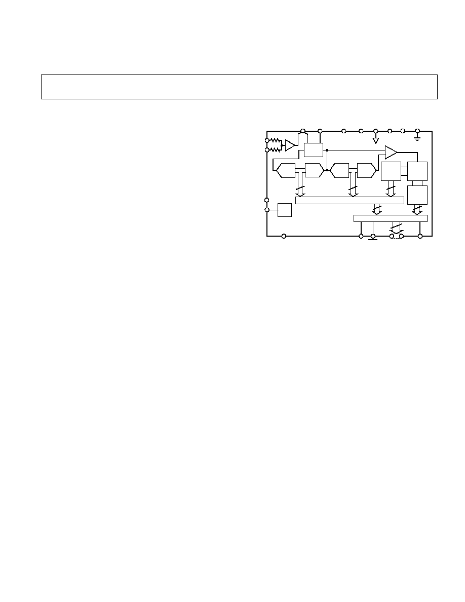
FUNCTIONAL BLOCK DIAGRAM
UPO/BPO
ENCODE
OTR
SHA
OUT
AIN1
S/H
2.5V
REF
REF OUT
REF IN
LATCHES
CORRECTION LOGIC
8-BIT
LADDER
MATRIX
AD1671
3
3-BIT
FLASH
REF COM
AIN2
5k
5k
V
CC
ACOM
V
EE
V
LOGIC
DCOM
3-BIT
FLASH
DAC
FINE
4-BIT
FLASH
COARSE
4-BIT
FLASH
4
DAC
3
12
MSB
DAV
BIT 1 12
4
8
X4
RANGE
SELECT
REV. B
Information furnished by Analog Devices is believed to be accurate and
reliable. However, no responsibility is assumed by Analog Devices for its
use, nor for any infringements of patents or other rights of third parties
which may result from its use. No license is granted by implication or
otherwise under any patent or patent rights of Analog Devices.
a
Complete 12-Bit 1.25 MSPS
Monolithic A/D Converter
AD1671
One Technology Way, P.O. Box 9106, Norwood, MA 02062-9106, U.S.A.
Tel: 617/329-4700
Fax: 617/326-8703
FEATURES
Conversion Time: 800 ns
1.25 MHz Throughput Rate
Complete: On-Chip Sample-and-Hold Amplifier and
Voltage Reference
Low Power Dissipation: 570 mW
No Missing Codes Guaranteed
Signal-to-Noise Plus Distortion Ratio
f
IN
= 100 kHz: 70 dB
Pin Configurable Input Voltage Ranges
Twos Complement or Offset Binary Output Data
28-Pin DIP and 28-Pin Surface Mount Package
Out of Range Indicator
PRODUCT DESCRIPTION
The AD1671 is a monolithic 12-bit, 1.25 MSPS analog-to-
digital converter with an on-board, high performance sample-
and-hold amplifier (SHA) and voltage reference. The AD1671
guarantees no missing codes over the full operating tempera-
ture range. The combination of a merged high speed bipolar/
CMOS process and a novel architecture results in a combi-
nation of speed and power consumption far superior to pre-
viously available hybrid implementations. Additionally, the
greater reliability of monolithic construction offers improved
system reliability and lower costs than hybrid designs.
The fast settling input SHA is equally suited for both multi-
plexed systems that switch negative to positive full-scale
voltage levels in successive channels and sampling inputs at
frequencies up to and beyond the Nyquist rate. The AD1671
provides both reference output and reference input pins, al-
lowing the on-board reference to serve as a system reference.
An external reference can also be chosen to suit the dc accu-
racy and temperature drift requirements of the application.
The AD1671 uses a subranging flash conversion technique,
with digital error correction for possible errors introduced in
the first part of the conversion cycle. An on-chip timing gen-
erator provides strobe pulses for each of the four internal
flash cycles. A single ENCODE pulse is used to control the
converter. The digital output data is presented in twos
complement or offset binary output format. An out-of-range
signal indicates an overflow condition. It can be used with
the most significant bit to determine low or high overflow.
The performance of the AD1671 is made possible by using high
speed, low noise bipolar circuitry in the linear sections and low
power CMOS for the logic sections. Analog Devices' ABCMOS-1
process provides both high speed bipolar and 2-micron CMOS
devices on a single chip. Laser trimmed thin-film resistors are
used to provide accuracy and temperature stability.
The AD1671 is available in two performance grades and three
temperature ranges. The AD1671J and K grades are available
over the 0
°
C to +70
°
C temperature range. The AD1671A grade
is available over the 40
°
C to +85
°
C temperature range. The
AD1671S grade is available over the 55
°
C to +125
°
C tempera-
ture range.
PRODUCT HIGHLIGHTS
The AD1671 offers a complete single chip sampling 12-bit,
1.25 MSPS analog-to-digital conversion function in a 28-pin
package.
The AD1671 at 570 mW consumes a fraction of the power of
currently available hybrids.
An OUT OF RANGE output bit indicates when the input sig-
nal is beyond the AD1671's input range.
Input signal ranges are 0 V to +5 V unipolar or
±
5 V bipolar,
selected by pin strapping, with an input resistance of 10 k
.
The input signal range can also be pin strapped for 0 V to +2.5 V
unipolar or
±
2.5 V bipolar with an input resistance of 10 M
.
Output data is available in unipolar, bipolar offset or bipolar
twos complement binary format.

DC SPECIFICATIONS
AD1671J/A/S
AD1671K
Parameter
Min
Typ
Max
Min
Typ
Max
Units
RESOLUTION
12
12
Bits
CONVERSION TIME
800
800
ns
ACCURACY
Integral Nonlinearity (INL)
±
1.5
±
2.5
±
0.7
±
2.5
LSB
(S Grade)
±
3.0
Differential Nonlinearity (DNL)
11
12
Bits
No Missing Codes
11 Bits Guaranteed
12 Bits Guaranteed
Unipolar Offsets
1
(+25
°
C)
±
9
±
9
LSB
Bipolar Zero
1
(+25
°
C)
±
10
±
10
LSB
Gain Error
1, 2
(+25
°
C)
0.1
0.35
0.1
0.35
% FSR
TEMPERATURE COEFFICIENTS
3
Unipolar Offset
±
25
±
25
ppm/
°
C
(S Grade)
±
25
Bipolar Zero
±
25
±
25
ppm/
°
C
(S Grade)
±
30
Gain Error
3
±
30
±
30
ppm/
°
C
(S Grade)
±
40
Gain Error
4
±
20
±
20
ppm/
°
C
POWER SUPPLY REJECTION
5
V
CC
(+5 V
±
0.25 V)
±
4
±
4
LSB
(S Grade)
±
5
V
LOGIC
(+5 V
±
0.25 V)
±
4
±
4
LSB
(S Grade)
±
5
V
EE
(5 V
±
0.25 V)
±
4
±
4
LSB
(S Grade)
±
5
ANALOG INPUT
Input Ranges
Bipolar
2.5
+2.5
2.5
+2.5
Volts
5.0
+5.0
5.0
+5.0
Volts
Unipolar
0
+2.5
0
+2.5
Volts
0
+5.0
0
+5.0
Volts
Input Resistance
(0 V to +2.5 V or
±
2.5 V Range)
10
10
M
(0 V to +5.0 V or
±
5 V Range)
8
10
12
8
10
12
k
Input Capacitance
10
10
pF
Aperture Delay
15
15
ns
Aperture Jitter
20
20
ps
INTERNAL VOLTAGE REFERENCE
Output Voltage
2.475
2.5
2.525
2.475
2.5
2.525
Volts
Output Current
Unipolar Mode
+2.5
+2.5
mA
Bipolar Mode
+1.0
+1.0
mA
LOGIC INPUTS
High Level Input Voltage, V
IH
2.0
2.0
Volts
Low Level Input Voltage, V
IL
0.8
0.8
Volts
High Level Input Current, I
IH
(V
IN
= V
LOGIC
)
10
+10
10
+10
µ
A
Low Level Input Current, I
LL
(V
IN
= 0 V)
10
+10
10
+10
µ
A
Input Capacitance, C
IN
5
5
pF
LOGIC OUTPUTS
High Level Output Voltage, V
OH
(I
OH
= 0.5 mA)
2.4
2.4
Volts
Low Level Output Voltage, V
OL
(I
OL
= 1.6 mA)
0.4
0.4
Volts
POWER SUPPLIES
Operating Voltages
V
CC
+4.75
+5.25
+4.75
+5.25
Volts
V
LOGIC
+4.5
+5.5
+4.5
+5.5
Volts
V
EE
4.75
5.25
4.75
5.25
Volts
Operating Current
I
CC
55
68
55
68
mA
I
LOGIC
6
3
5
3
5
mA
I
EE
55
68
55
68
mA
POWER CONSUMPTION
570
750
570
750
mW
TEMPERATURE RANGE (SPECIFIED)
J/K
0
+70
0
+70
°
C
A
40
+85
40
+85
°
C
S
55
+125
55
+125
°
C
NOTES
1
Adjustable to zero with external potentiometers.
2
Includes internal voltage reference error.
3
+25
°
C to T
MIN
and +25
°
C to T
MAX
4
Excludes internal reference drift.
5
Change in gain error as a function of the dc supply voltage.
6
Tested under static conditions. See Figure 15 for typical curve of I
LOGIC
vs. load capacitance at maximum t
C
.
Specifications subject to change without notice.
(T
MIN
to T
MAX
with V
CC
= +5 V 5%, V
LOGIC
= +5 V 10%, V
EE
= 5 V 5%, unless otherwise noted)
AD1671SPECIFICATIONS
REV. B
2
AD1671
(T
MIN
to T
MAX
with V
CC
= +5 V 5%, V
LOGIC
= +5 V 10%, V
EE
= 5 V 5%, f
SAMPLE
= 1 MSPS,
f
lNPUT
= 1OO kHz, unless otherwise noted)
1
AC SPECIFICATIONS
AD1671J/A/S
AD1671K
Parameter
Min
Typ
Max
Min
Typ
Max
Units
SIGNAL-TO-NOISE PLUS DISTORTION RATIO
(S/N + D)
0.5 dB Input
68
70
68
71
dB
20 dB Input
50
51
dB
EFFECTIVE NUMBER OF BITS (ENOB)
11.2
11.2
Bits
TOTAL HARMONIC DISTORTION (THD)
80
75
83
75
dB
PEAK SPURIOUS OR PEAK HARMONIC COMPONENT
80
77
81
77
dB
SMALL SIGNAL BANDWIDTH
12
12
MHz
FULL POWER BANDWIDTH
2
2
MHz
INTERMODULATION DISTORTION (IMD)
2
2nd Order Products
80
75
80
75
dB
3rd Order Products
85
75
85
75
dB
NOTES
1
f
IN
amplitude = 0.5 dB (9.44 V p-p) bipolar mode full scale unless otherwise indicated. All measurements referred to a 0 dB (
±
5 V) input signal, unless otherwise
indicated.
2
f
A
= 99 kHz, f
B
= 100 kHz with f
SAMPLE
= 1 MSPS.
Specifications subject to change without notice.
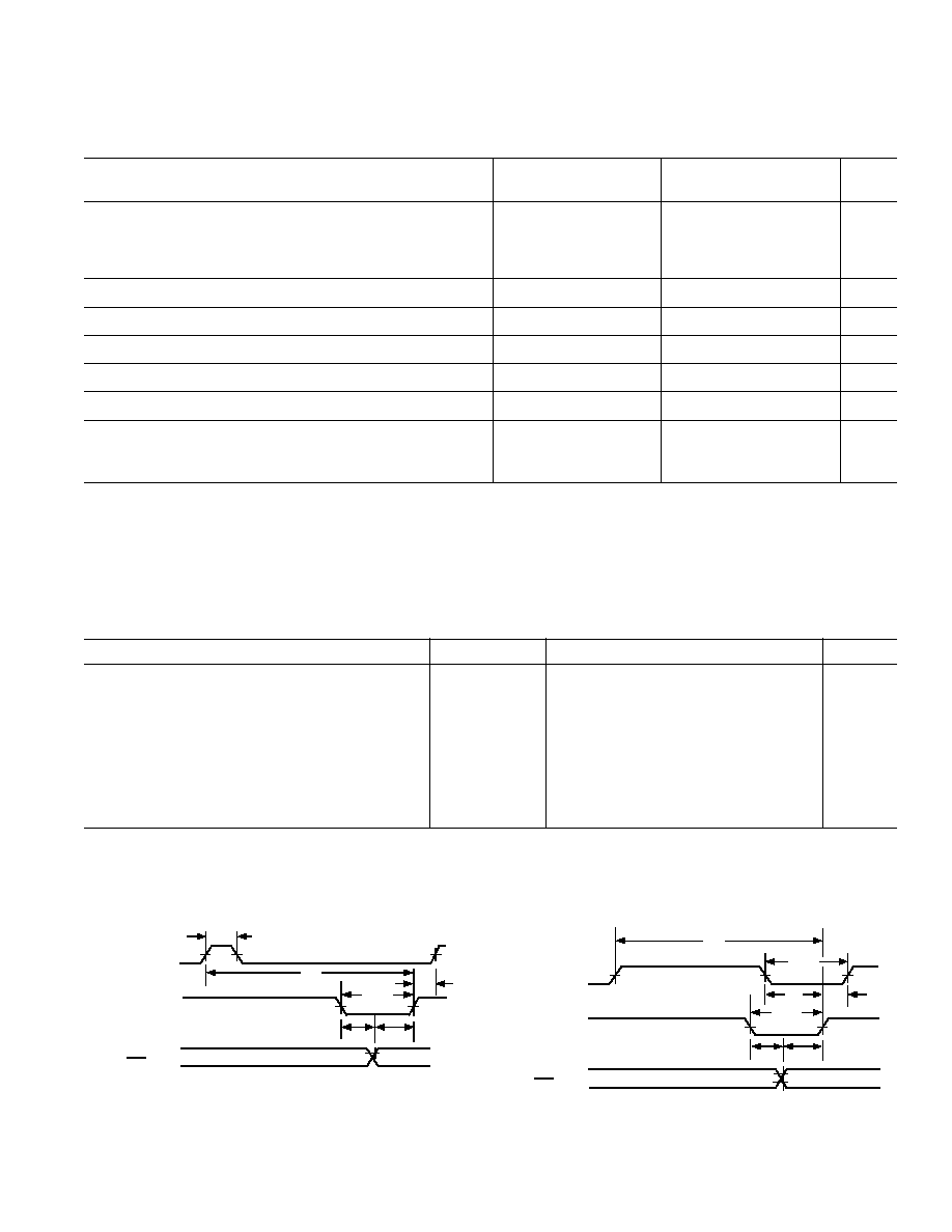
SWITCHING SPECIFICATIONS
Parameters
Symbol
Min
Typ
Max
Units
Conversion Time
t
C
800
ns
Sample Rate
F
S
1.25
MSPS
ENCODE Pulse Width High (Figure 1a)
t
ENC
20
50
ns
ENCODE Pulse Width Low (Figure 1b)
t
ENCL
20
ns
DAV Pulse Width
t
DAV
150
300
ns
ENCODE Falling Edge Delay
t
F
0
ns
Start New Conversion Delay
t
R
0
ns
Data and OTR Delay from DAV Falling Edge
t
DD
1
20
75
ns
Data and OTR Valid before DAV Rising Edge
t
SS
2
20
75
ns
NOTES
1
t
DD
is measured from when the falling edge of DAV crosses 0.8 V to when the output crosses 0.4 V or 2.4 V with a 25 pF load capacitor on each output pin.
2
t
SS
is measured from when the outputs cross 0.4 V or 2.4 V to when the rising edge of DAV crosses 2.4 V with a 25 pF load capacitor on each output pin.
Specifications subject to change without notice.
(For all grades T
MIN
to T
MAX
with V
CC
= +5 V 5%, V
LO61C
= +5 V 10%,
V
EE
= 5 V 5%; V
IL
= 0.8 V, V
IH
= 2.0 V, V
OL
= 0.4 V and V
OH
= 2.4 V)
ENCODE
DAV
DATA 0 (PREVIOUS)
DATA 1
C
t
DAV
t
DD
t
SS
t
t
F
t
R
t
ENCL
BIT 112
MSB, OTR
Figure 1b. Encode Pulse LOW
ENCODE
DAV
DATA 0 (PREVIOUS)
DATA 1
ENC
t
C
t
DAV
t
DD
t
SS
t
R
t
BIT 112
MSB, OTR
Figure 1a. Encode Pulse HIGH
REV. B
3
AD1671
REV. B
4
PIN DESCRIPTION
Symbol
Pin No.
Type
Name and Function
ACOM
27
P
Analog Ground.
AIN
22, 23
AI
Analog Inputs, AIN1 and AIN2. The AD1671 can be pin strapped for four input ranges:
Range
Pin Strap
Signal Input
0 to +2.5 V,
±
2.5 V
Connect AIN1 to AIN2
AIN1 or AIN2
0 to +5 V,
±
5 V
Connect AIN1 or AIN2 to ACOM
AIN1 or AIN2
BIT 1 (MSB)
13
DO
Most Significant Bit.
BIT 2BIT 11
12-3
DO
Data Bits 2 through 11.
BIT 12 (LSB)
2
DO
Least Significant Bit.
BPO/UPO
26
AI
Bipolar or Unipolar Configuration Pin. See section on Input Range Connections for details.
DAV
16
DO
Data Available Output. The rising edge of DAV indicates an end of conversion and can be used
to latch current data into an external register. The falling edge of DAV can be used to latch
previous dam into an external register.
DCOM
19
P
Digital Ground.
ENCODE
17
DI
The analog input is sampled on the rising edge of ENCODE.
MSB
14
DO
Inverted Most Significant Bit. Provides twos complement output data format.
OTR
15
DO
Out of Range is Active HIGH when the analog input is out of range. See Output Data Format,
Table III.
REF COM
20
AI
REF COM is the internal reference ground pin. REF COM should be connected as indicated
in the Grounding and Decoupling Rules and Optional External Reference Connection Sections.
REF IN
24
AI
REF IN is the external 2.5 V reference input.
REF OUT
21
AO
REF OUT is the internal 2.5 V reference output.
SHA OUT
25
AO
No Connect for bipolar input ranges. Connect SHA OUT to BPO/UPO for unipolar input ranges.
V
CC
28
P
+5 V Analog Power.
V
EE
1
P
5 V Analog Power.
V
LOGIC
18
P
+5 V Digital Power.
TYPE: AI = Analog Input; AO = Analog Output; DI = Digital Input; DO = Digital Outputs; P = Power.
PIN CONFIGURATION
ACOM
BPO/UPO
DCOM
ENCODE
DAV
OTR
MSB
BIT 12 (LSB)
BIT 11
BIT 10
BIT 9
BIT 8
BIT 7
BIT 6
BIT 5
BIT 4
BIT 3
BIT 2
BIT 1 (MSB)
AIN1
REF COM
REF OUT
AIN2
SHA OUT
1
2
3
7
28
27
26
22
8
9
10
21
20
19
11
12
18
17
4
5
25
24
6
23
TOP VIEW
(Not to Scale)
13
14
16
15
AD1671
V
EE
V
CC
V
LOGIC
REF IN

AD1671
REV. B
5
ABSOLUTE MAXIMUM RATINGS*
Parameter
With Respect to
Min
Max
Units
V
CC
ACOM
0 5
+6.5
Volts
V
EE
ACOM
6.5
+0.5
Volts
V
LOGIC
DCOM
0.5
+6.5
Volts
ACOM
DCOM
1.0
+1.0
Volts
V
CC
V
LOGIC
6.5
+6.5
Volts
ENCODE
DCOM
0.5
V
LOGIC
+ 0.5 Volts
REF IN
ACOM
0.5
V
CC
+ 0.5
Volts
AIN
ACOM
11.0
+11.0
Volts
BPO/UPO
ACOM
0.5
V
CC
+ 0.5
Volts
Junction Temperature
+150
°
C
Storage Temperature
65
+150
°
C
Lead Temperature (10 sec)
+300
°
C
*Stresses above those listed under "Absolute Maximum Ratings" may cause
permanent damage to the device. This is a stress rating only and functional
operation of the device at these or any other conditions above those indicated in
the operational sections of this specification is not implied. Exposure to absolute
maximum ratings for extended periods may effect device reliability.
WARNING!
ESD SENSITIVE DEVICE
CAUTION
ESD (electrostatic discharge) sensitive device. Electrostatic charges as high as 4000 V readily
accumulate on the human body and test equipment and can discharge without detection.
Although the AD1671 features proprietary ESD protection circuitry, permanent damage may
occur on devices subjected to high energy electrostatic discharges. Therefore, proper ESD
precautions are recommended to avoid performance degradation or loss of functionality.
ORDERING GUIDE
Temperature
Package
Model
1
Linearity
Range
Option
2, 3
AD1671JQ
±
2.5 LSB
0
°
C to +70
°
C
Q-28
AD1671KQ
±
2 LSB
0
°
C to +70
°
C
Q-28
AD1671JP
±
2.5 LSB
0
°
C to +70
°
C
P-28A
AD1671KP
±
2 LSB
0
°
C to +70
°
C
P-28A
AD1671AQ
±
2.5 LSB
40
°
C to +85
°
C
Q-28
AD1671AP
±
2.5 LSB
40
°
C to +85
°
C
P-28A
AD1671SQ
±
3 LSB
55
°
C to +125
°
C
Q-28
NOTES
1
For details on grade and package offerings screened in accordance with
MIL-STD-883, refer to Analog Devices' Military Products Databook or
current AD1671/883 data sheet.
2
P = Plastic Leaded Chip Carrier, Q = Cerdip.
3
Analog Devices reserves the right to ship side brazed ceramic packages in
lieu of cerdip.

AD1671
REV. B
6
DEFINITIONS OF SPECIFICATIONS
INTEGRAL NONLINEARITY (INL)
Integral nonlinearity refers to the deviation of each individual
code from a line drawn from "zero" through "full scale." The
point used as "zero" occurs 1/2 LSB (1.22 mV for a 10 V span)
before the first code transition (all zeros to only the LSB on).
"Full-scale" is defined as a level 1 1/2 LSB beyond the last code
transition (to all ones). The deviation is measured from the low
side transition of each particular code to the true straight line.
DIFFERENTIAL LINEARITY ERROR (NO MISSING
CODES)
An ideal ADC exhibits code transitions that are exactly 1 LSB
apart. DNL is the deviation from the ideal value. Thus every
code has a finite width. Guaranteed no missing codes to 11- or
12-bit resolution indicates that all 2048 and 4096 codes, respec-
tively, must be present over all operating ranges. No missing
codes to 11 bits (in the case of a 12-bit resolution ADC) also
means that no two consecutive codes are missing.
UNIPOLAR OFFSET
The first transition should occur at a level 1/2 LSB above analog
common. Unipolar offset is defined as the deviation of the ac-
tual from that point. This offset can be adjusted as discussed
later. The unipolar offset temperature coefficient specifies the
maximum change of the transition point over temperature, with
or without external adjustments.
BIPOLAR ZERO
In the bipolar mode the major carry transition (0111 1111 1111 to
1000 0000 0000) should occur for an analog value 1/2 LSB be-
low analog common. The bipolar offset error and temperature
coefficient specify the initial deviation and maximum change in
the error over temperature.
GAIN ERROR
The last transition (from 1111 1111 1110 to 1111 1111 1111)
should occur for an analog value 1 1/2 LSB below the nominal
full scale (4.9963 volts for 5.000 volts full scale). The gain error
is the deviation of the actual level at the last transition from the
ideal level. The gain error can be adjusted to zero as shown in
Figures 4 through 7.
TEMPERATURE COEFFICIENTS
The temperature coefficients for unipolar offset, bipolar zero
and gain error specify the maximum change from the initial
(+25
°
C) value to the value at T
MIN
or T
MAX
.
POWER SUPPLY REJECTION
One of the effects of power supply error on the performance of
the device will be a small change in gain. The specifications
show the maximum full-scale change from the initial value with
the supplies at the various limits.
DYNAMIC SPECIFICATIONS
SIGNAL-TO-NOISE PLUS DISTORTION (S/ N+D) RATIO
S/N+D is the ratio of the rms value of the measured input signal
to the rms sum of all other spectral components, including har-
monics but excluding dc. The value for S/N+D is expressed in
decibels.
EFFECTIVE NUMBER OF BITS (ENOB)
ENOB is calculated from the expression (S/N+D) = 6.02N +
1.76 dB, where N is equal to the effective number of bits.
TOTAL HARMONIC DISTORTION (THD)
THD is the ratio of the rms sum of the first six harmonic com-
ponents to the rms value of the measured input signal and is ex-
pressed as a percentage or in decibels.
INTERMODULATION DISTORTION (IMD)
With inputs consisting of sine waves at two frequencies, fa and
fb, any device with nonlinearities will create distortion products
of order (m + n), at sum and difference frequencies of mfa
±
nfb, where m, n = 0, 1, 2, 3. . . . Intermodulation terms are
those for which m or n is not equal to zero. For example, the
second order terms are (fa + fb) and (fa fb), and the third or-
der terms are (2 fa + fb), (2 fa fb), (fa + 2 fb) and (2fb fa).
The IMD products are expressed as the decibel ratio of the rms
sum of the measured input signals to the rms sum of the distor-
tion terms. The two signals are of equal amplitude and the peak
value of their sum is 0.5 dB from full scale. The IMD products
are normalized to a 0 dB input signal.
PEAK SPURIOUS OR PEAK HARMONIC COMPONENT
The peak spurious or peak harmonic component is the largest
spectral component, excluding the input signal and dc. This
value is expressed in decibels relative to the rms value of a full-
scale input signal.
APERTURE DELAY
Aperture delay is the difference between thc switch delay and
the analog delay of the SHA. This delay represents the point in
time, relative to the rising edge of ENCODE input, that the
analog input is sampled.
APERTURE JITTER
Aperture jitter is the variation in aperture delay for successive
samples.
FULL POWER BANDWIDTH
The input frequency at which the amplitude of the recon-
structed fundamental is reduced by 3 dB for a full-scale input.
AD1671
REV. B
7
THEORY OF OPERATION
The AD1671 uses a successive subranging architecture. The
analog-to-digital conversion takes place in four independent
steps or flashes. The sampled analog input signal is subranged
to an intermediate residue voltage for the final 12-bit result by
utilizing multiple flashes with subtraction DACs (see the AD1671
functional block diagram).
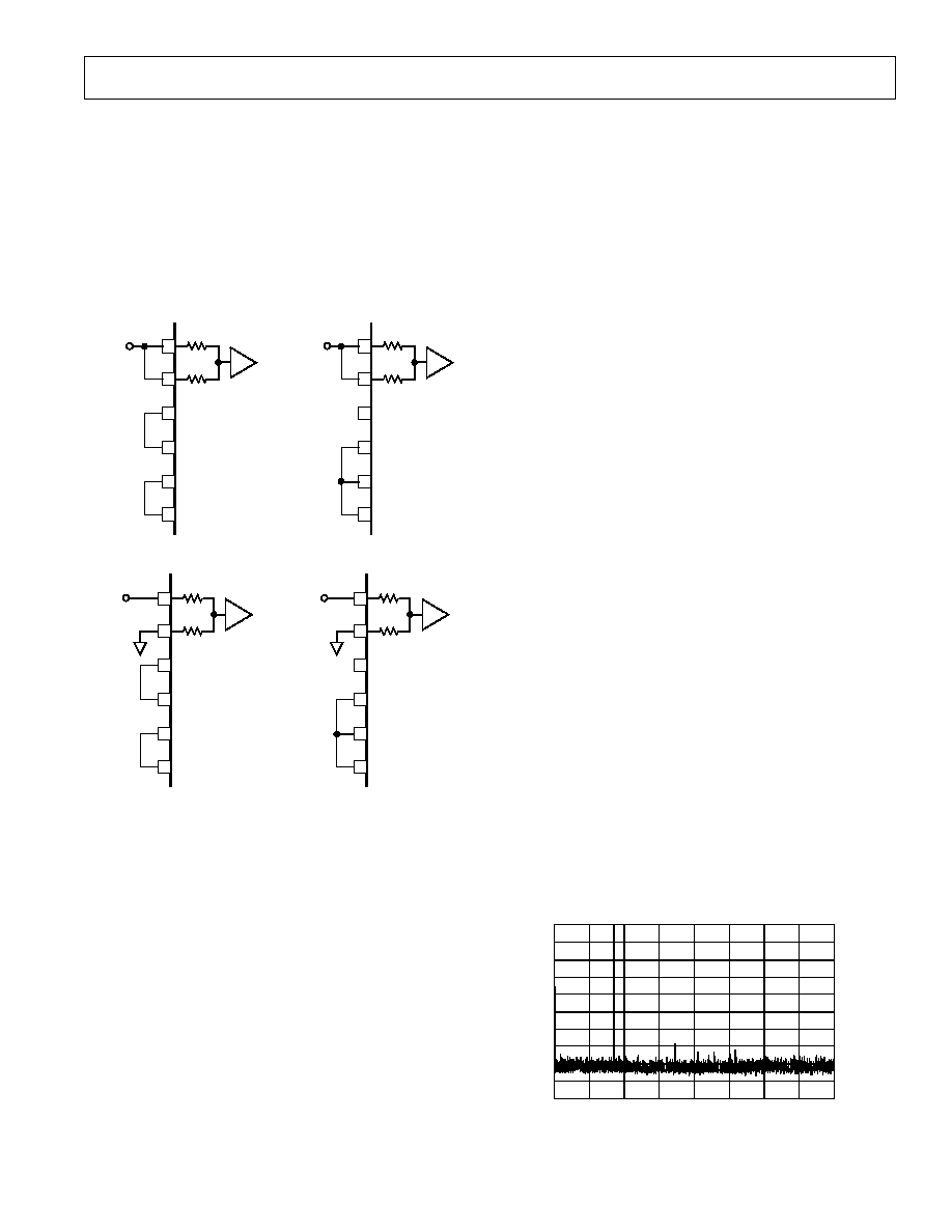
The AD1671 can be configured to operate with unipolar (0 V to
+5 V, 0 V to +2.5 V) or bipolar (
±
5 V,
±
2.5 V) inputs by con-
necting AIN (Pins 22, 23), SHA OUT (Pin 25) and BPO/UPO
(Pin 26) as shown in Figure 2.
2.5V
TO
+2.5V
AIN1
AIN2
5k
5k
SHA OUT
BPO/UPO
AD1671
REF IN
REF OUT
SHA
AIN1
AIN2
5k
5k
SHA OUT
BPO/UPO
AD1671
REF IN
REF OUT
0
TO
+2.5V
SHA
a. 0 V to +2.5V Input Range b.
±
2.5 V Input Range
AIN1
AIN2
5k
5k
SHA OUT
BPO/UPO
AD1671
REF IN
REF OUT
±
5V
SHA
AIN1
AIN2
5k
5k
SHA OUT
BPO/UPO
AD1671
REF IN
REF OUT
0
TO
+5V
SHA
c. 0 V to +5 V Input Range d.
±
5 V Input Range
Figure 2. AD1671 Input Range Connections
The AD1671 conversion cycle begins by simply providing an
active HIGH level on the ENCODE pin (Pin 17). The rising
edge of the ENCODE pulse starts the conversion. The falling
edge of the ENCODE pulse is specified to operate within a win-
dow of time, less than 50 ns after the rising edge of ENCODE
or after the falling edge of DAV. The time window prevents
digitally coupled noise from being introduced during the final
stages of conversion. An internal timing generator circuit accu-
rately controls SHA, flash and DAC timing.
Upon receipt of an ENCODE command the input voltage is
held by the front-end SHA and the first 3-bit flash converts the
analog input voltage. The 3-bit result is passed to a correction
logic register and a segmented current output DAC. The DAC
output is connected through a resistor (within the Range/Span
Select Block) to SHA OUT. A residue voltage is created by sub-
tracting the DAC output from SHA OUT, which is less than
one eighth of the full-scale analog input. The second flash has
an input range that is configured with one bit of overlap with the
previous DAC. The overlap allows for errors during the flash
conversion. The first residue voltage is connected to the second
3-bit flash and to the noninverting input of a high speed, differ-
ential, gain of eight amplifier. The second flash result is passed
to the correction logic register and to the second segmented cur-
rent output DAC. The output of the second DAC is connected
to the inverting input of the differential amplifier. The differen-
tial amplifier output is connected to a two-step, backend, 8-bit
flash. This 8-bit flash consists of coarse and fine flash convert-
ers. The result of the coarse 4-bit flash converter, also config-
ured to overlap one bit of DAC 2, is connected to the correction
logic register and selects one of 16 resistors from which the fine
4-bit flash will establish its span voltage. The fine 4-bit flash is
connected directly to the output latches.
The internal timing generator automatically places the SHA into
the acquire mode when DAV goes LOW. Upon completion of
conversion (when DAV is set HIGH), the SHA has acquired the
analog input to the specified level of accuracy and will remain in
the sample mode until the next ENCODE command.
The AD1671 will flag an out-of-range condition when the input
voltage exceeds the analog input range. OTR (Pin 15) is active
HIGH when an out-of-range high or low condition exists. Bits
112 are HIGH when the analog input voltage is greater than
the selected input range and LOW when the analog input is less
than the selected input range.
AD1671 DYNAMIC PERFORMANCE
The AD1671 is specified for dc and dynamic performance. A
sampling converter's dynamic performance reflects both quan-
tizer and sample-and-hold amplifier (SHA) performance. Quan-
tizer nonlinearities, such as INL and DNL, can degrade dynamic
performance. However, a SHA is the critical element which has to
accurately sample fast slewing analog input signals. The AD1671's
high performance, low noise, patented on-chip SHA minimizes
distortion and noise specifications. Nonlinearities are minimized
by using a fast slewing, low noise architecture and subregulation
of the sampling switch to provide constant offsets (therefore
reducing input signal dependent nonlinearities).
Figure 3 is a typical 2k point Fast Fourier Transform (FFT)
plot of a 100 kHz input signal sampled at 1 MHz. The funda-
mental amplitude is set at 0.5 dB to avoid input signal clipping
of offset or gain errors. Note the total harmonic distortion is ap-
proximately 81 dB, signal to noise plus distortion is 71 dB and
the spurious free dynamic range is 84 dB.
SIGNAL AMPLITUDE dB
0
100
50
75
25
FREQUENCY
0
Figure 3. AD1671 FFT Plot, f
IN
= 100 kHz, f
SAMPLE
= 1 MHz
AD1671
REV. B
8
85
40
0
50
45
45
50
55
60
65
70
75
80
5
10
15
20
25
30
35
40
ANALOG INPUT dB
SPURIOUS FREE DYNAMIC RANGE dB
Figure 7. Spurious Free Dynamic Range vs. Input
Amplitude, f
IN
= 250 kHz
APPLYING THE AD1671
GROUNDING AND DECOUPLING RULES
Proper grounding and decoupling should be a primary design
objective in any high speed, high resolution system. The
AD1671 separates analog and digital grounds to optimize the
management of analog and digital ground currents in a system.
The AD1671 is designed to minimize the current flowing from
REF COM (Pin 20) by directing the majority of the current
from V
CC
(+5 VPin 28) to V
EE
(5 VPin 1). Minimizing ana-
log ground currents hence reduces the potential for large ground
voltage drops. This can be especially true in systems that do not
utilize ground planes or wide ground runs. REF COM is also
configured to be code independent, therefore reducing input de-
pendent analog ground voltage drops and errors. Code depen-
dent ground current is diverted to ACOM (Pin 27). Also critical
in any high speed digital design is the use of proper digital
grounding techniques to avoid potential CMOS "ground
bounce." Figure 3 is provided to assist in the proper layout,
grounding and decoupling techniques.
AIN1
REF IN
BPO/UPO
ACOM
BIT 1
BIT 12
DCOM
AD1671
ENCODE
DAV
OTR
MSB
AGP*
DGP*
+5V
5V
*GROUND PLANE RECOMMENDED
AIN2
REF OUT
SHA OUT
REF COM
1
µ
F
V
CC
V
EE
V
LOGIC
V (
±
5V)
IN
1
18
28
+5V
0.1
µ
F
10
µ
F
23
22
20
27
19
25
26
24
21
13
2
17
16
15
14
0.1
µ
F
10
µ
F
0.1
µ
F
10
µ
F
Figure 8. AD1671 Grounding and Decoupling
Figure 4 plots both S/(N+D) and Effective Number of Bits
(ENOB) for a 100 kHz input signal sampled from 666 kHz to
1.25 MHz.
SAMPLING FREQUENCY kHz
72.5
68
1250
68.5
70.5
714
666
69
69.5
70
71
71.5
72
1111
1000
909
833
769
S/(N+D) dB
11.75
11.50
11.25
11.00
EFFECTIVE NUMBER OF BITS
Figure 4. S/(N/D) vs. Sampling Frequency, f
IN
= 100 kHz
Figure 5 is a THD plot for a full-scale 100 kHz input signal with
the sample frequency swept from 666 kHz to 1.25 MHz.
68
86
1250
84
76
714
666
82
80
78
74
72
70
1111
1000
909
833
769
SAMPLING FREQUENCY kHz
THD dB
Figure 5. THD vs. Sampling Rate, f
IN
= 100 kHz
The AD1671's SFDR performance is ideal for use in communi-
cation systems such as high speed modems and digital radios.
The SFDR is better than 84 dB with sample rates up to 1.11 MHz
and increases as the input signal amplitude is attenuated by ap-
proximately 3 dB. Note also the SFDR is typically better than
80 dB with input signals attenuated by up to 7 dB.
1250
714
666
1111
1000
909
833
769
SAMPLING FREQUENCY kHz
SPURIOUS FREE DYNAMIC RANGE dB
86
68
84
76
82
80
78
74
72
70
88
90
Figure 6. Spurious Free Dynamic Range vs. Sampling
Rate, f
IN
= 100 kHz
AD1671
REV. B
9
Table I is a list of grounding and decoupling rules that should
be reviewed before laying out a printed circuit board.
Table I. Grounding and Decoupling Guidelines
Power Supply
Decoupling
Comment
Capacitor Values
0.1
µ
F (Ceramic) and 1
µ
F
(Tantalum) Surface Mount Chip
Capacitors Recommended to
Reduce Lead Inductance
Capacitor Locations
Directly at Positive and Negative
Supply Pins to Common Ground
Plane
Reference (REF OUT)
Capacitor Value
1
µ
F (Tantalum) to ACOM
Grounding
Analog Ground
Ground Plane or Wide Ground
Return Connected to the Analog
Power Supply
Reference Ground
Critical Common Connections
(REF COM)
Should be Star Connected to REF
COM (as Shown in Figure 8)
Digital Ground
Ground Plane or Wide Ground
Return Connected to the Digital
Power Supply
Analog and Digital Ground Connected Together Once at the
AD1671
UNIPOLAR (0 V TO +5 V) CALIBRATION
The AD1671 is factory trimmed to minimize offset, gain and
linearity errors. In some applications the offset and gain errors
of the AD1671 need to be externally adjusted to zero. This is
accomplished by trimming the voltage at AIN2 (Pin 22). The
circuit in Figure 9 is recommended for calibrating offset and
gain errors of the AD1671 when configured in the 0 V to +5 V
input range. If the offset trim resistor R1 is used, it should be
trimmed as follows, although a different offset can be set for a
particular system requirement. This circuit will give approxi-
mately
±
5 mV of offset trim range. Nominally the AD1671 is
intended to have a 1/2 LSB offset so that the exact analog input
for a given code will be in the middle of that code (halfway be-
tween the transitions to the codes above it and below it). Thus,
the first transition (from 0000 0000 0000 to 0000 0000 0001)
will occur for an input level of +1/2 LSB (0.61 mV for 5 V
range).
The gain trim is done by applying a signal 1 1/2 LSBs below the
nominal full scale (4.998 V for a 5 V range). Trim R2 to give
the last transition (1111 1111 1110 to 1111 1111 1111). This
circuit will give approximately
±
0.5% FS of adjustment range.
R2
50
GAIN
ADJ
AIN1
AIN2
5k
5k
SHA OUT
BPO/UPO
AD1671
REF IN
REF OUT
SHA
1µF
50k
+5V
5V
OFFSET
ADJ
R1
10k
25
0 TO +5V
V
IN
Figure 9. Unipolar (0 V to +5 V) Calibration
BIPOLAR ( 5 V) CALIBRATION
The connections for the bipolar
±
5 V input range is shown in
Figure 10.
R2
50
GAIN
ADJ
AIN1
AIN2
5k
5k
SHA OUT
BPO/UPO
AD1671
REF IN
REF OUT
SHA
1µF
50k
+5V
5V
OFFSET
ADJ
R1
10k
25
V
IN
5V TO +5V
Figure 10. Bipolar (
±
5 V) Calibration
Bipolar calibration is similar to unipolar calibration. First, a sig-
nal 1/2 LSB above negative full scale (4.9988 V) is applied and
R1 is trimmed to give the first transition (0000 0000 0000 to
0000 0000 0001). Then a signal 1 1/2 LSB below positive full
scale (+4.9963 V) is applied and R2 is trimmed to give the last
transition (1111 1111 1110 to 1111 1111 1111).
AD1671
REV. B
10
UNIPOLAR (0 V TO +2.5 V) CALIBRATION
The connections for the 0 V to +2.5 V input range calibration is
shown in Figure 11. Figure 11 shows an example of how the
offset error can be trimmed in front of the AD1671. The proce-
dure for trimming the offset and gain errors is the same as for
the unipolar 5 V range.
AIN1
AIN2
5k
5k
SHA OUT
BPO/UPO
AD1671
REF IN
REF OUT
SHA
OFFSET ADJ
+15V
1k
0 TO +2.5V
V
IN
10k
10k
R2
2k
GAIN
ADJ
1µF
R1
AD845
1k
390
Figure 11. Unipolar (0 V to +2.5 V) Calibration
BIPOLAR ( 2.5 V) CALIBRATION
The connections for the bipolar
±
2.5 V input range is shown in
Figure 12.
AIN1
AIN2
5k
5k
SHA OUT
BPO/UPO
AD1671
REF IN
REF OUT
SHA
OFFSET ADJ
+15V
1k
V
IN
10k
10k
R2
2k
GAIN
ADJ
1µF
R1
AD845
1k
390
2.5V TO +2.5V
Figure 12. Bipolar (
±
2.5 V) Calibration
OUTPUT LATCHES
Figure 13 shows the AD1671 connected to the 74HC574 octal
D-type edge-triggered latches with 3-state outputs. The latch
can drive highly capacitive loads (i.e., bus lines, I/O ports) while
maintaining the data signal integrity. The maximum setup and
hold times of the 574 type latch must be less than 20 ns (t
DD
and t
SS
minimum). To satisfy the requirements of the 574 type
latch the recommended logic families are S, AS, ALS, F or
BCT. New data from the AD1671 is latched on the rising edge
of the DAV (Pin 16) output pulse. Previous data can be latched
by inverting the DAV output with a 7404 type inverter.
BIT 1
BIT 2
BIT 3
BIT 4
BIT 5
BIT 6
BIT 7
BIT 8
BIT 9
BIT 10
BIT 11
BIT 12
DAV
DATA BUS
3-STATE
CONTROL
AD1671
1D
2D
3D
4D
5D
6D
7D
8D
CLOCK
1Q
2Q
3Q
4Q
5Q
6Q
7Q
8Q
74HC574
OC
1D
2D
3D
4D
5D
6D
7D
8D
CLOCK
1Q
2Q
3Q
4Q
5Q
6Q
7Q
8Q
74HC574
OC
Figure 13. AD1671 to Output Latches
OUT OF RANGE
An out-of-range condition exists when the analog input voltage
is beyond the input range (0 V to +2.5 V, 0 V to +5 V,
±
2.5 V,
±
5 V) of the converter OTR (Pin 15) is set low when the analog
input voltage is within the analog input range. OTR is set HIGH
and will remain HIGH when the analog input voltage exceeds
the input range by typically 1/2 LSB (OTR transition is tested to
±
6 LSBs of accuracy) from the center of the
±
full-scale output
codes. OTR will remain HIGH until the analog input is within
the input range and another conversion is completed. By logical
ANDing OTR with the MSB and its complement, overrange
high or underrange low conditions can be detected. Table II is a
truth table for the over/under range circuit in Figure 14. Sys-
tems requiring programmable gain conditioning prior to the
AD1671 can immediately detect an out-of-range condition, thus
eliminating gain selection iterations.
Table II. Out-of-Range Truth Table
OTR
MSB
Analog Input Is
0
0
In Range
0
1
In Range
1
0
Underrange
1
1
Overrange
MSB
OTR
MSB
OVER = "1"
UNDER = "1"
Figure 14. Overrange or Underrange Logic
AD1671
REV. B
11
Table III. Output Data Format
Input
Analog
Digital
Range
Coding
Input
l
Output
OTR
2
0 V to +2.5 V
Straight Binary
0.0003 V
0000 0000 0000
1
0 V
0000 0000 0000
0
+2.5 V
1111 1111 1111
0
+2.5003 V
1111 1111 1111
1
0 V to +5 V
Straight Binary
0.0006 V
0000 0000 0000
1
0 V
0000 0000 0000
0
+5 V
1111 1111 1111
0
+5.0006 V
1111 1111 1111
1
2.5 V to +2.5 V
Offset Binary
2.5006 V
0000 0000 0000
1
2.5 V
0000 0000 0000
0
+2.5 V
1111 1111 1111
0
+2.4994 V
1111 1111 1111
1
5 V to +5 V
Offset Binary
5.0012 V
0000 0000 0000
1
5 V
0000 0000 0000
0
+5 V
1111 1111 1111
0
+4.9988 V
1111 1111 1111
1
2.5 V to +2.5 V
Twos Complement
2.5006 V
1000 0000 0000
1
(Using MSB)
2.5 V
1000 0000 0000
0
+2.5 V
0111 1111 1111
0
+2.4994 V
0111 1111 1111
1
5 V to +5 V
Twos Complement
5.0012 V
1000 0000 0000
1
(Using MSB)
5 V
1000 0000 0000
0
+5 V
0111 1111 1111
0
+4.9988 V
0111 1111 1111
1
NOTES
1
Voltages listed are with offset and gain errors adjusted to zero.
2
Typical performance.
OUTPUT DATA FORMAT
The AD1671 provides both MSB and MSB outputs, delivering
data in positive true straight binary for unipolar input ranges
and positive true offset binary or twos complement for bipolar
input ranges. Straight binary coding is used for systems that ac-
cept positive-only signals. If straight binary coding is used with
bipolar input signals, a 0 V input would result in a binary output
of 2048. The application software would have to subtract 2048
to determine the true input voltage. Host registers typically per-
form math on signed integers and assume data is in that format.
Twos complement format minimizes software overhead which is
especially important in high speed data transfers, such as a
DMA operation. The CPU is not bogged down performing data
conversion steps, hence the total system throughput is increased.
OPTIONAL EXTERNAL REFERENCE
The AD1671 includes an onboard +2.5 V reference. The refer-
ence input pin (REF IN) can be connected to reference output
pin (REF OUT) or a standard external +2.5 V reference can be
selected to meet specific system requirements. Fast switching in-
put dependent currents are modulated at the reference input.
The reference input voltage can be held with the use of a capaci-
tor. To prevent the AD1671's onboard reference from oscil-
lating when not connected to REF IN, REF OUT must be
connected to +5 V. It is possible to connect REF OUT to +5 V
due to its output circuit implementation which shuts down the
reference.
I
LOGIC
VS. CONVERSION RATE
Figure 15 is the typical logic supply current vs. conversion rate
for various capacitor loads on the digital outputs.
6.5
6.0
5.5
5.0
4.5
4.0
3.5
3.0
2.5
2.0
1.5
1.0
0.5
1M
CONVERSION RATE Hz
mA
1k
10k
100k
CL = 50pF
CL = 30pF
CL = 0pF
Figure 15. I
LOGIC
vs. Conversion Rate for Various
Capacitive Loads on the Digital Outputs
AD1671
REV. B
12
APPLICATIONS
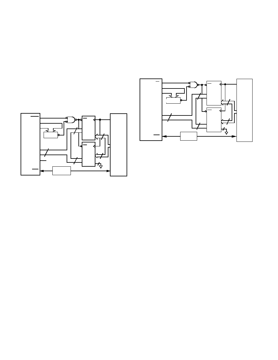
AD1671 TO ADSP-2100A
Figure 16 demonstrates the AD1671 to ADSP-2100A interface.
The 2100A with a clock frequency of 12.5 MHz can execute an
instruction in one 80 ns cycle. The AD1671 is configured to
perform continuous time sampling. The DAV output of the
AD1671 is asserted at the end of each conversion. DAV can be
used to latch the conversion result into the two 574 octal
D-latches. The falling edge of the sampling clock is used to
generate an interrupt (IRQ3) for the processor. Upon interrupt,
the ADSP-2100A starts a data memory read by providing an
address on the DMA bus. The decoded address generates OE
for the latches and the processor reads their output over the
DMA bus. The conversion result is read within a single proces-
sor cycle.
+5V
ADSP-
2100A
DMA0:13
DMA0:15
DMACK
ADDRESS BUS
Q0:7
D0:7
574
OE
Q0:7
D0:7
574
OE
DATA BUS
D0:3
DAV
BIT1:12
ENCODE
16
8
4
8
4
DMRD
IRQ3
AD1671
SAMPLING
CLOCK
DECODE
8
Figure 16. AD1671 to ADSP-2100A Interface
AD1671 TO ADSP-2101/2102
Figure 17 is identical to the 2100A interface except the sam-
pling clock is used to generate an interrupt (IRQ2) for the pro-
cessor. Upon interrupt the ADSP-2100A starts a data memory
read by providing an address on the address (A) bus. The de-
code address generates OE for the D-latches and the processor
reads their output over the Data (D) bus. Reading the conver-
sion result is thus completed within a single processor cycle.
ADSP-2101
A0:13
D0:15
ADDRESS BUS
DECODE
Q0:7
D0:7
574
OE
Q0:7
D0:7
574
OE
DATA BUS
D0:3
16
8
4
8
8
4
RD
IRQ2
SAMPLING
CLOCK
DAV
BIT1:12
ENCODE
AD1671
Figure 17. AD1671 to ADSP-2101/ADSP-2102 Interface

AD1671
REV. B
13
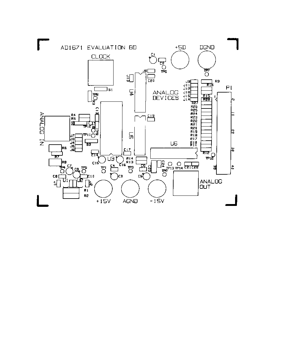
COMPONENT LIST
Parts List
Type
Reference Designator
Description
R1, R2
Resistor, 5%, 0.5 W, 100
R3, R4, R5
Resistor, 1%, 49.9
R6
100
Trim Potentiometer
R7
Resistor 1%, 4.99 k
Optional
R8
X
Trim Potentiometer, Optional
R9, R11
Resistor, 1%, 4.99 k
R10
Resistor, 1%, 10 k
R12
Resistor, 1%, 2.49 k
R13
Resistor, 1%, 787
R14
Resistor, 1%, 249
R15R28
Resistor, 5%, 22
C1, C3, C5
Cap, Tantalum, 22
µ
F
C2, C4, C6, C8, C10
Cap, Ceramic, 0.01
µ
F
C7, C9, C15, C16
Cap, Tantalum, 10
µ
F
C11, C12, C13, C14, C17
Cap, Ceramic, 0.1
µ
F
C18
Cap, Ceramic, 1.0
µ
F
C19C22
Cap, Ceramic, 0.1
µ
F
C23
Cap, Mica, 100 pF
C24
Cap, Ceramic, 0.001
µ
F
U1
78L05 +5 V Regulator
U2
79L05 5 V Regulator
U3
AD1671
U4U5
74HC573 Drivers
U6
AD568
W1W3
BNC Jacks
J1J15
Jumpers and Headers
Metal Binding Posts
S1
Wide 28-Pin Socket
S2
Narrow 20-Pin Socket
S3
Narrow 24-Pin Socket
SW1SW3
SECMA SPDT Switch
TP1, TP2, TP4TP6
Test Point, Red
TP3, TP7, TP10, TP13
Test Point, Black
TP8, TP9, TP11, TP12, TP14
Test Point, White
P1
40-Pin Connector Male + Hooks
AD1671
REV. B
14
Figure 18. AD1671/EB PCB Layout--Silkscreen Layer
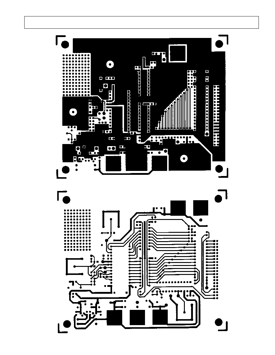
AD1671
REV. B
15
Figure 19. AD1671/EB PCB Layout--Component Side
Figure 20. AD1671/EB PCB Layout--Solder Side
AD1671
REV. B
16
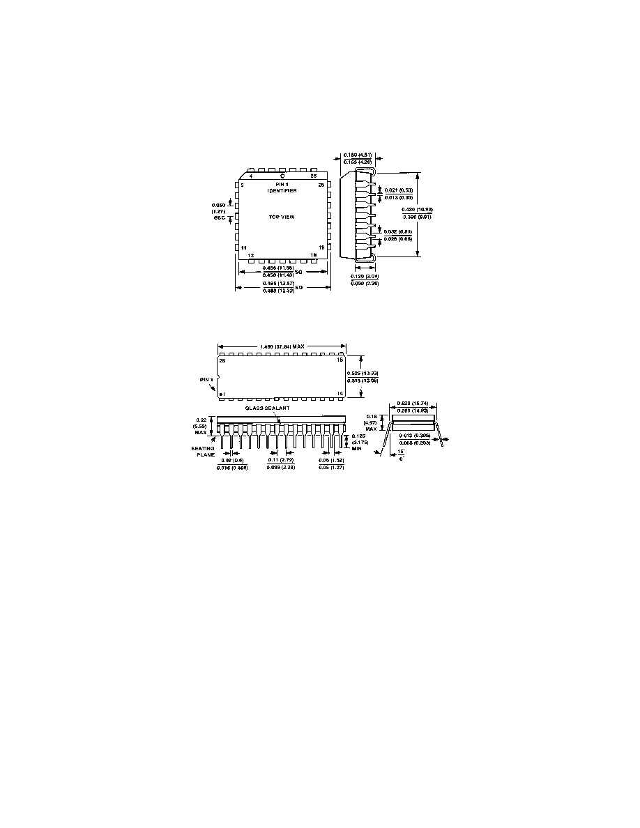
OUTLINE DIMENSIONS
Dimensions shown in inches and (mm).
28-Lead PLCC (P-28A) Package
28-Pin Cerdip (Q-28) Package
C1616a1010/93
PRINTED IN U.S.A.