/home/web/htmldatasheet/RUSSIAN/html/ad/164578
REV. 0
Information furnished by Analog Devices is believed to be accurate and
reliable. However, no responsibility is assumed by Analog Devices for its
use, nor for any infringements of patents or other rights of third parties that
may result from its use. No license is granted by implication or otherwise
under any patent or patent rights of Analog Devices.
a
ADR420/ADR421
One Technology Way, P.O. Box 9106, Norwood, MA 02062-9106, U.S.A.
Tel: 781/329-4700
www.analog.com
Fax: 781/326-8703
© Analog Devices, Inc., 2001
Ultraprecision Low Noise, 2.048 V/2.500 V
XFET
®
Voltage References
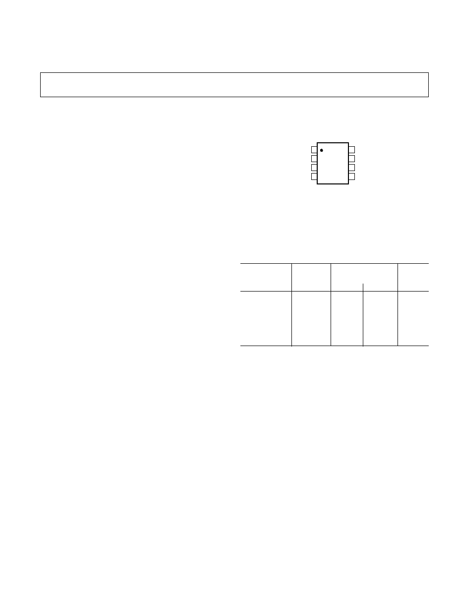
PIN CONFIGURATION
Surface-Mount Packages
8-Lead SOIC
8-Lead Mini_SOIC
TOP VIEW
(Not to Scale)
8
7
6
5
1
2
3
4
NIC =
TP =
TP
V
IN
NIC
GND
TP
NIC
V
OUT
TRIM
ADR420/
ADR421
NO INTERNAL CONNECTION
TEST PIN
(DO NOT CONNECT)
FEATURES
Low Noise 1.75 V p-p (0.1 Hz to 10 Hz)
Low Temperature Coefficient: 3 ppm/ C
Long-Term Stability: 50 ppm/1000 Hours
Load Regulation: 70 ppm/mA
Line Regulation: 35 ppm/V
Low Hysteresis: 40 ppm Typical
Wide Operating Range
ADR420: 4 V to 18 V
ADR421: 4.5 V to 18 V
Quiescent Current: 0.5 mA Max
High Output Current: 10 mA
Wide Temperature Range: 40 C to +125 C
APPLICATIONS
Precision Data Acquisition Systems
High-Resolution Converters
Battery-Powered Instrumentation
Portable Medical Instruments
Industrial Process Control Systems
Precision Instruments
Optical Network Control Circuits
Table I. ADR42x Products
Output
Voltage
Initial Accuracy
Tempco
Model
V
O
mV
%
ppm/ C
ADR420AR
2.048
3
0.15
10
ADR420BR
2.048
1
0.05
3
ADR420ARM
2.048
3
0.15
10
ADR421AR
2.50
3
0.12
10
ADR421BR
2.50
1
0.04
3
ADR421ARM
2.50
3
0.12
10
GENERAL DESCRIPTION
The ADR420 and ADR421 are precision 2.048 V and 2.500 V
XFET voltage references featuring low noise, high accuracy and
stability, and low power consumption in a SOIC and Mini_SOIC
footprint. Patented temperature drift curvature correction tech-
niques and XFET (eXtra implanted junction FET) technology
minimize nonlinearity of the voltage change with temperature.
The wide operating range and low power consumption make
them ideal for 5 V battery-powered applications.
The ADR420 and ADR421 trim terminal can be used to adjust
the output voltage over a
± 0.5% range without affecting the
temperature coefficient.
The ADR420 and ADR421 are low power, very low drift volt-
age references that provide an extremely stable output voltage
from a wide supply voltage range. They are specified over the
extended industrial (40
°C to +125°C) temperature range.
XFET is a registered trademark of Analog Devices, Inc.
REV. 0
2
ADR420/ADR421SPECIFICATIONS
ADR420 ELECTRICAL SPECIFICATIONS
Parameter
Symbol
Conditions
Min
Typ
Max
Unit
Output Voltage
A Grade
V
O
2.045
2.048
2.051
V
Initial Accuracy
V
OERR
3
+3
mV
0.15
+0.15
%
Output Voltage
B Grade
V
O
2.047
2.048
2.049
V
Initial Accuracy
V
OERR
1
+1
mV
0.05
+0.05
%
Temperature Coefficient A Grade
TCV
O
40
°C < T
A
< +125
°C
2
10
ppm/
°C
B Grade
1
3
ppm/
°C
Supply Voltage Headroom
V
IN
V
O
2
V
Line Regulation
V
O
/
V
IN
V
IN
= 5 V to 18 V
10
35
ppm/V
40
°C < T
A
< +125
°C
Load Regulation
V
O
/
I
LOAD
I
LOAD
= 0 mA to 10 mA
70
ppm/mA
40
°C < T
A
< +125
°C
Quiescent Current
I
IN
No Load
390
500
µA
40
°C < T
A
< +125
°C
600
µA
Voltage Noise
e
N
p-p
0.1 Hz to 10 Hz
1.75
µV p-p
Voltage Noise Density
e
N
1 kHz
60
nV/
Hz
Turn-On Settling Time
t
R
10
µs
Long-Term Stability
V
O
1000 Hours
50
ppm
Output Voltage Hysteresis
V
O_HYS
40
ppm
Ripple Rejection Ratio
RRR
f
IN
= 10 kHz
90
dB
Short Circuit to GND
I
SC
27
mA
Specifications subject to change without notice.
(@ V
IN
= 5.0 V to 15.0 V, T
A
= 25 C, unless otherwise noted.)
ADR421 ELECTRICAL SPECIFICATIONS
Parameter
Symbol
Conditions
Min
Typ
Max
Unit
Output Voltage
A Grade
V
O
2.497
2.500
2.503
V
Initial Accuracy
V
OERR
3
+3
mV
0.12
+0.12
%
Output Voltage
B Grade
V
O
2.499
2.500
2.501
V
Initial Accuracy
V
OERR
1
+1
mV
0.04
+0.04
%
Temperature Coefficient A Grade
TCV
O
40
°C < T
A
< +125
°C
2
10
ppm/
°C
B Grade
1
3
ppm/
°C
Supply Voltage Headroom
V
IN
V
O
2
V
Line Regulation
V
O
/
V
IN
V
IN
= 5 V to 18 V
10
35
ppm/V
40
°C < T
A
< +125
°C
Load Regulation
V
O
/
I
LOAD
I
LOAD
= 0 mA to 10 mA
70
ppm/mA
40
°C < T
A
< +125
°C
Quiescent Current
I
IN
No Load
390
500
µA
40
°C < T
A
< +125
°C
600
µA
Voltage Noise
e
N
p-p
0.1 Hz to 10 Hz
1.75
µV p-p
Voltage Noise Density
e
N
1 kHz
80
nV/
Hz
Turn-On Settling Time
t
R
10
µs
Long-Term Stability
V
O
1000 Hours
50
ppm
Output Voltage Hysteresis
V
O_HYS
40
ppm
Ripple Rejection Ratio
RRR
f
IN
= 10 kHz
60
dB
Short Circuit to GND
I
SC
27
mA
Specifications subject to change without notice.
(@ V
IN
= 5.0 V to 15.0 V, T
A
= 25 C, unless otherwise noted.)
REV. 0
ADR420/ADR421
3
CAUTION
ESD (electrostatic discharge) sensitive device. Electrostatic charges as high as 4000 V readily
accumulate on the human body and test equipment and can discharge without detection. Although the
ADR420/ADR421 features proprietary ESD protection circuitry, permanent damage may occur on
devices subjected to high-energy electrostatic discharges. Therefore, proper ESD precautions are
recommended to avoid performance degradation or loss of functionality.
WARNING!
ESD SENSITIVE DEVICE
ABSOLUTE MAXIMUM RATINGS
1
Supply Voltage . . . . . . . . . . . . . . . . . . . . . . . . . . . . . . . . . 18 V
Output Short-Circuit Duration to GND
. . . . . . . . . . . . . . . . . . . . . . . . . . . . . . . . . . . . . . . Indefinite
Storage Temperature Range
R, RM Package . . . . . . . . . . . . . . . . . . . . 65
°C to +150°C
Operating Temperature Range
ADR420/ADR421 . . . . . . . . . . . . . . . . . . 40
°C to +125°C
Junction Temperature Range
R, RM Package . . . . . . . . . . . . . . . . . . . . 65
°C to +150°C
Lead Temperature Range (Soldering, 60 sec) . . . . . . . . 300
°C
ORDERING GUIDE
Output
Temperature
Voltage
Initial Accuracy
Coefficient (Max)
Package
Package
Number of
Temperature
Top
Model
V
O
mV
%
ppm/ C
V/ C
Description
Option
per Reel
Range C
Mark
ADR420AR
2.048
3
0.15
10
20
SOIC
R-8
98
40 to +125
ADR420AR-Reel7
2.048
3
0.15
10
20
SOIC
R-8
1,000
40 to +125
ADR420BR
2.048
1
0.05
3
6
SOIC
R-8
98
40 to +125
ADR420BR-Reel7
2.048
1
0.05
3
6
SOIC
R-8
1,000
40 to +125
ADR420ARM-Reel7
2.048
3
0.15
10
20
Mini_SOIC
RM-8
1,000
40 to +125
R4A
ADR421AR
2.50
3
0.12
10
25
SOIC
R-8
98
40 to +125
ADR421AR-Reel7
2.50
3
0.12
10
25
SOIC
R-8
1,000
40 to +125
ADR421BR
2.50
1
0.04
3
7.5
SOIC
R-8
98
40 to +125
ADR421BR-Reel7
2.50
1
0.04
3
7.5
SOIC
R-8
1,000
40 to +125
ADR421ARM-Reel7
2.50
3
0.12
10
25
Mini_SOIC
RM-8
1,000
40 to +125
R5A
Package Type
JA
2
Unit
8-Lead Mini_SOIC (RM)
190
°C/W
8-Lead SOIC (R)
130
°C/W
NOTES
1
Absolute maximum ratings apply at 25
°C, unless otherwise noted.
2
JA
is specified for the worst-case conditions, i.e.,
JA
is specified for device soldered
in circuit board for surface-mount packages.
PIN FUNCTION DESCRIPTIONS
Pin
Mnemonic
Description
1, 8
TP
Test Pin. There are actual connections in
TP pins but they are reserved for factory
testing purposes. Users should not con-
nect anything to TP pins, otherwise the
device may not function properly.
2
V
IN
This is the input voltage (5 V to 15 V).
3, 7
NIC
No Internal Connect. NICs have no inter-
nal connections.
4
GND
Ground Pin = 0 V.
5
TRIM
Trim Terminal. It can be used to adjust the
output voltage over a
±0.5% range without
affecting the temperature coefficient.
6
V
OUT
Output Voltage.
PIN CONFIGURATION
TOP VIEW
(Not to Scale)
8
7
6
5
1
2
3
4
NIC =
TP =
TP
V
IN
NIC
GND
TP
NIC
V
OUT
TRIM
ADR420/
ADR421
NO INTERNAL CONNECTION
TEST PIN
(DO NOT CONNECT)

REV. 0
ADR420/ADR421
4
PARAMETER DEFINITIONS:
Temperature Coefficient
The change of output voltage over the operating temperature
range and normalized by the output voltage at 25
°C, expressed
in ppm/
°C. The equation follows:
TCV
ppm C
V T
V T
V
C
T
T
O
O
O
O
/
(
)
( )
(
) (
)
°
(
)
=
° ×
×
2
1
2
1
6
25
10
where
V
O
(25
°C) = V
O
at 25
°C
V
O
(T
1
) = V
O
at Temperature 1
V
O
(T
2
) = V
O
at Temperature 2.
Line Regulation
The change in output voltage due to a specified change in input
voltage. It includes the effects of self-heating. Line regulation is
expressed in either percent per volt, parts-per-million per volt,
or microvolts per volt change in input voltage
Load Regulation
The change in output voltage due to a specified change in load
current. It includes the effects of self-heating. Load Regulation
is expressed in either microvolts per milliampere, parts-per-million
per milliampere, or ohms of dc output resistance.
Long-Term Stability
Typical shift of output voltage at 25
°C on a sample of parts
subjected to operation life test of 1000 hours at 125
°C:
V
V
t
V
t
V
ppm
V
t
V
t
V
t
O
O
O
O
O
O
O
=
=
×
( )
( )
(
)
( )
( )
( )
0
1
0
1
0
6
10
where
V
O
(t
0
) = V
O
at 25
°C at Time 0
V
O
(t
1
) = V
O
at 25
°C after 1000 hours operation at 125°C.
Thermal Hysteresis
Thermal Hysteresis is defined as the change of output voltage
after the device is cycled through temperature from +25
°C to
40
°C to +125°C and back to +25°C. This is a typical value
from a sample of parts put through such a cycle.
V
V
C
V
V
ppm
V
C
V
V
C
O
HYS
O
O TC
O
HYS
O
O TC
O
_
_
_
_
(
)
(
)
(
)
(
)
=
°
=
°
°
×
25
25
25
10
6
where
V
O
(25
°C) = V
O
at 25
°C
V
O_TC
= V
O
at 25
°C after temperature cycle at +25°C to 40°C
to +125
°C and back to +25°C.
NOTES
Input Capacitor
Input capacitors are not required on the ADR420/ADR421. There
is no limit for the value of the capacitor used on the input, but
a 1
µF to 10 µF capacitor on the input will improve transient
response in applications where the supply suddenly changes. An
additional 0.1
µF in parallel will also help reducing noise from
the supply.
Output Capacitor
The ADR420/ADR421 does not need output capacitors for
stability under any load condition. An output capacitor, typical
0.1
µF, will filter out any low-level noise voltage and will not affect
the operation of the part. On the other hand, the load transient
response can be improved with an additional 1
µF to 10 µF output
capacitor in parallel. A capacitor here will act as a source of stored
energy for sudden increase in load current. The only parameter
that will degrade, by adding an output capacitor, is turn-on time
and it depends on the size of the capacitor chosen.
REV. 0
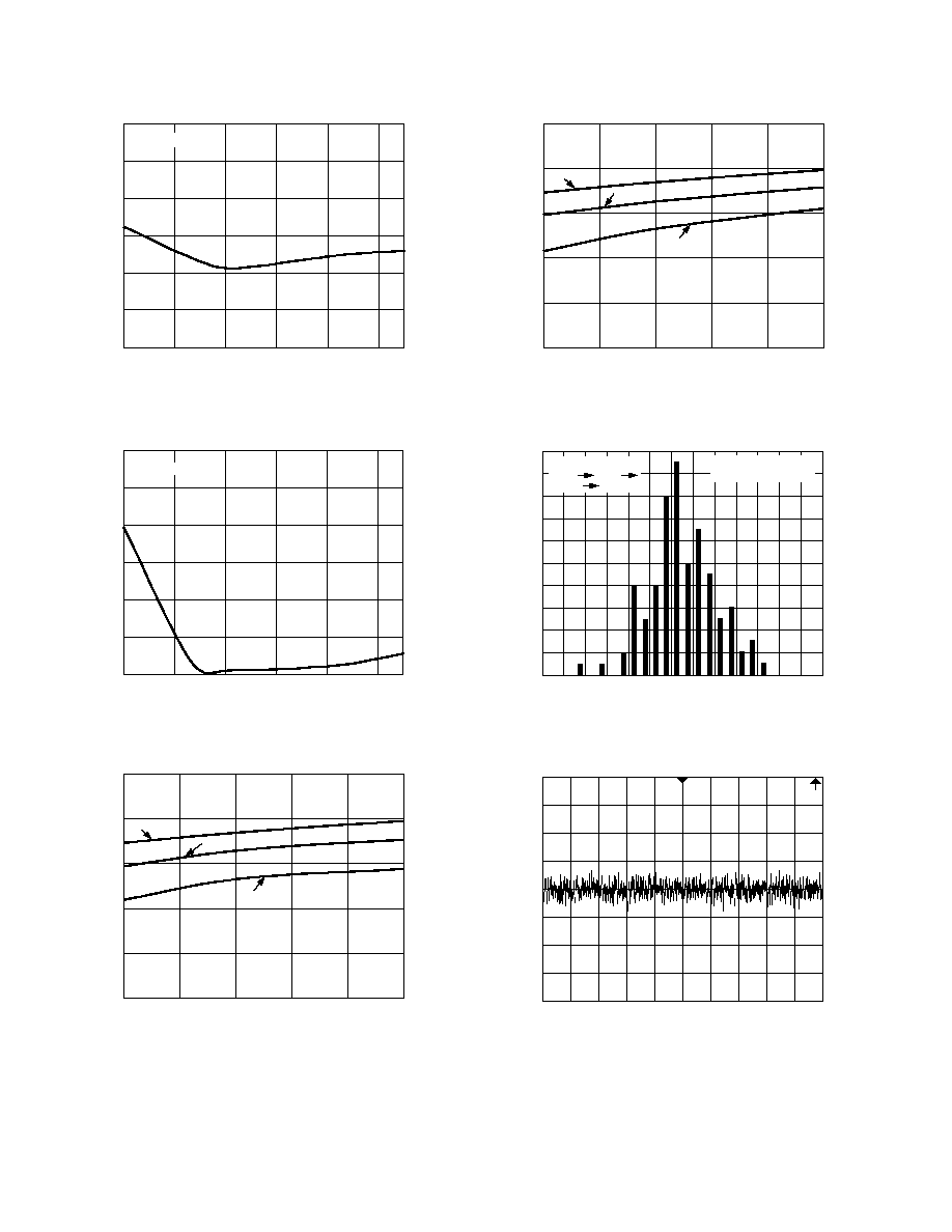
Typical Performance CharacteristicsADR420/ADR421
2.0495
2.0493
2.0491
2.0489
2.0487
2.0485
2.0483
2.0481
2.0479
2.0477
2.0475
40 10 20 50 80 110 125
TEMPERATURE C
V
OUT
V
TPC 1. ADR420 Typical Output Voltage vs. Temperature
2.4995
2.4997
2.4999
2.5001
2.5003
2.5005
2.5007
2.5009
2.5011
2.5013
2.5015
40
10
20
50
80
110
125
TEMPERATURE C
V
OUT
V
TPC 2. ADR421 Typical Output Voltage vs. Temperature
INPUT VOLTAGE V
0.25
4
SUPPL
Y CURRENT
mA
6
8
10
12
14
15
0.30
0.35
0.40
0.45
0.50
0.55
+125 C
+25 C
40 C
TPC 3. ADR420 Supply Current vs. Input Voltage
INPUT VOLTAGE V
0.25
4
SUPPL
Y CURRENT
mA
6
8
10
12
14
15
0.30
0.35
0.40
0.45
0.50
0.55
+125 C
+25 C
40 C
TPC 4. ADR421 Supply Current vs. Input Voltage
TEMPERATURE C
0
40
LO
AD REGULA
T
ION
ppm/mA
10
20
50
80
110
125
10
20
30
40
50
60
70
I
L
= 0 TO 5mA
V
IN
= 4.5V
V
IN
= 6V
TPC 5. ADR420 Load Regulation vs. Temperature
TEMPERATURE C
0
40
LO
AD REGULA
T
ION
ppm/mA
10
20
50
80
110
125
10
20
30
40
50
60
70
I
L
= 0 TO 5mA
V
IN
= 5V
V
IN
= 6.5V
TPC 6. ADR421 Load Regulation vs. Temperature
5
REV. 0
ADR420/ADR421
6
0
1
2
3
4
5
6
40
10
20
50
80
110
TEMPERATURE C
125
LINE REGULATION
ppm/V
V
IN
= 4.5V TO 15V
TPC 7. ADR420 Line Regulation vs. Temperature
0
1
2
3
4
5
6
40
10
20
50
80
110
TEMPERATURE C
L
INE REGULATION
ppm/V
125
V
IN
= 5V TO 15V
TPC 8. ADR421 Line Regulation vs. Temperature
LOAD CURRENT mA
0
0
DIFFERENTIAL V
O
L
T
A
GE
V
1
2
3
4
5
0.5
1.0
1.5
2.0
2.5
40 C
+25 C
+85 C
TPC 9. ADR420 Minimum Input-Output Voltage Differen-
tial vs. Load Current
LOAD CURRENT mA
0
0
DIFFERENTIAL V
O
L
T
A
GE
V
1
2
3
4
5
0.5
1.0
1.5
2.0
2.5
40 C
+25 C
+125 C
TPC 10. ADR421 Minimum Input-Output Voltage Differen-
tial vs. Load Current
DEVIATION mV
0
0.6
FREQ
UENCY
2
4
6
8
10
0.40
12
14
16
18
20
0.20
0
0.20
0.40
0.60 MORE
QUANTITY OF PARTS
IN SAMPLE 110
TEMPERATURE
+25 C 40 C
+125 C +25 C
TPC 11. ADR421 Typical Hysteresis
1
V
/DIV
TIME 1s/DIV
TPC 12. ADR421 Typical Noise Voltage 0.1 Hz to 10 Hz
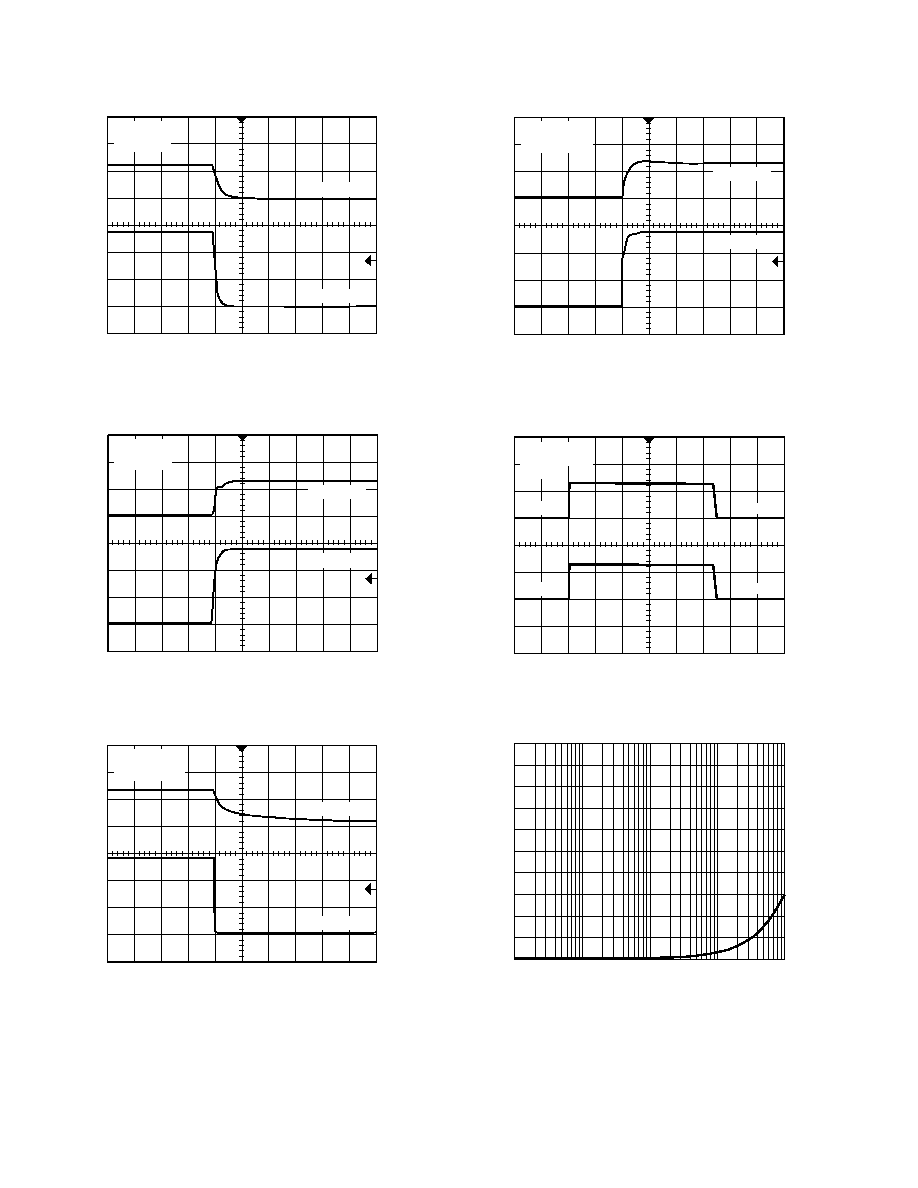
REV. 0
ADR420/ADR421
7
50
V/DIV
TIME 1s/DIV
TPC 13. Typical Noise Voltage 10 Hz to 10 kHz
FREQUENCY Hz
1000
100
10
10
10000
100
V
O
L
T
A
GE NOISE DENSITY
1000
ADR421
ADR420
TPC 14. Voltage Noise Density vs. Frequency
TIME 100 s/DIV
C
BYPASS
= 0 F
LINE INTERRUPTION
500mV/DIV
500mV/DIV
V
OUT
V
IN
TPC 15. ADR421 Line Transient Response
TIME 100 s/DIV
C
BYPASS
= 0.1 F
LINE INTERRUPTION
500mV/DIV
500mV/DIV
V
OUT
V
IN
TPC 16. ADR421 Line Transient Response
TIME 100 s/DIV
C
L
= 0 F
1mA LOAD
2V/DIV
1V/DIV
V
OUT
LOAD ON
LOAD OFF
TPC 17. ADR421 Load Transient Response
TIME 100 s/DIV
C
L
= 100nF
1mA LOAD
2V/DIV
1V/DIV
V
OUT
LOAD ON
LOAD OFF
TPC 18. ADR421 Load Transient Response
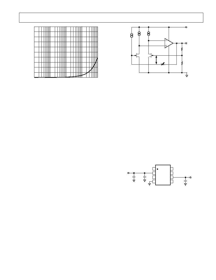
REV. 0
ADR420/ADR421
8
TIME 4 s/DIV
C
IN
= 0.01 F
NO LOAD
V
OUT
2V/DIV
V
IN
2V/DIV
TPC 19. ADR421 Turn-Off Response
TIME 4 s/DIV
C
IN
= 0.01 F
NO LOAD
V
OUT
2V/DIV
V
IN
2V/DIV
TPC 20. ADR421 Turn-On Response
TIME 4 s/DIV
C
LOAD
= 0.01 F
NO INPUT CAP
V
OUT
2V/DIV
V
IN
2V/DIV
TPC 21. ADR421 Turn-Off Response
TIME 4 s/DIV
C
LOAD
= 0.01 F
NO INPUT CAP
V
OUT
2V/DIV
V
IN
2V/DIV
TPC 22. ADR421 Turn-On Response
C
L
= 0
TIME 100 s/DIV
C
BYPASS
= 0.1 F
R
L
= 500
2V/DIV
5V/DIV
V
IN
V
OUT
TPC 23. ADR421 Turn-On/Turn-Off Response
FREQUENCY Hz
10
100k
100
OUTPUT IMPED
ANCE
1k
10k
10
5
15
20
25
30
35
40
45
50
TPC 24. ADR420 Output Impedance vs. Frequency
REV. 0
ADR420/ADR421
9
FREQUENCY Hz
10
100k
100
OUTPUT IMPED
ANCE
1k
10k
10
5
15
20
25
30
35
40
45
50
TPC 25. ADR421 Output Impedance vs. Frequency
THEORY OF OPERATION
The ADR42x series of references uses a new reference genera-
tion technique known as XFET (eXtra implanted junction
FET). This technique yields a reference with low supply cur-
rent, good thermal hysteresis, and exceptionally low noise.
The core of the XFET reference consists of two junction field-
effect transistors, one of which has an extra channel implant to
raise its pinch-off voltage. By running the two JFETs at the
same drain current, the difference in pinch-off voltage can be
amplified and used to form a highly stable voltage reference.
The intrinsic reference voltage is around 0.5 V with a negative
temperature coefficient of about 120 ppm/
°C. This slope is
essentially constant to the dielectric constant of silicon and can
be closely compensated by adding a correction term generated
in the same fashion as the proportional-to-temperature (PTAT)
term used to compensate bandgap references. The big advan-
tage over a bandgap reference is that the intrinsic temperature
coefficient is some thirty times lower (therefore requiring less
correction), which results in much lower noise since most of the
noise of a bandgap reference comes from the temperature com-
pensation circuitry.
Figure 1 shows the basic topology of the ADR42x series. The
temperature correction term is provided by a current source
with a value designed to be proportional to absolute tempera-
ture. The general equation is:
V
G
V
R
I
OUT
P
PTAT
= ×
-
×
(
)
1
where G is the gain of the reciprocal of the divider ratio,
V
P
is
the difference in pinch-off voltage between the two JFETs, and
I
PTAT
is the positive temperature coefficient correction current.
ADR420 and ADR421 are created by on-chip adjustment of
R2 and R3 to achieve 2.048 V or 2.500 V at the reference
output respectively.
V
IN
*
GND
V
OUT
ADR420/
ADR421
I
PTAT
V
OUT
= G( V
P
R1 I
PTAT
)
*EXTRA CHANNEL IMPLANT
V
P
R1
R3
R2
I
1
I
1
Figure 1. Simplified Schematic
Device Power Dissipation Considerations
The ADR42x family of references is guaranteed to deliver load
currents to 10 mA with an input voltage that ranges from 4.5 V
to 18 V. When these devices are used in applications at higher
current, users should account for the temperature effects due to
the power dissipation increases with the following equation:
T
P
T
D
A
A
J
J
=
×
+
where T
J
and T
A
are the junction and ambient temperatures,
respectively, P
D
is the device power dissipation, and
JA
is the
device package thermal resistance.
Basic Voltage Reference Connections
Voltage references, in general, require a bypass capacitor con-
nected from V
OUT
to GND. The circuit in Figure 2 illustrates
the basic configuration for the ADR42x family of references.
Other than a 0.1
µF capacitor at the output to help improve
noise suppression, a large output capacitor at the output is not
required for circuit stability.
10 F
TOP VIEW
(Not to Scale)
8
7
6
5
1
2
3
4
NIC = NO INTERNAL CONNECTION
TP = TEST PIN
(DO NOT CONNECT)
TP
NIC
TP
NIC
OUTPUT
ADR42x
0.1 F
TRIM
0.1 F
+
V
IN
Figure 2. Basic Voltage Reference Configuration
Noise Performance
The noise generated by the ADR42x family of references is
typically less than 2
µV p-p over the 0.1 Hz to 10 Hz band.
TPC 12 shows the 0.1 Hz to 10 Hz noise of the ADR421,
which is only 1.75
µV p-p. The noise measurement is made
with a bandpass filter made of a 2-pole high-pass filter with a
corner frequency at 0.1 Hz and a 2-pole low-pass filter with a
corner frequency at 10 Hz.
REV. 0
ADR420/ADR421
10
Turn-On Time
Upon application of power (cold start), the time required for the
output voltage to reach its final value within a specified error
band is defined as the turn-on settling time. Two components
normally associated with this are the time for the active circuits
to settle, and the time for the thermal gradients on the chip to
stabilize. TPC 19 to TPC 23 show the turn-on settling time for
the ADR421.
APPLICATIONS SECTION
OUTPUT ADJUSTMENT
The ADR420/ADR421 trim terminal can be used to adjust the
output voltage over a
± 0.5% range. This feature allows the
system designer to trim system errors out by setting the refer-
ence to a voltage other than the nominal. This is also helpful if
the part is used in a system at temperature to trim out any error.
Adjustment of the output has negligible effect on the tempera-
ture performance of the device. To avoid degrading temperature
coefficient, both the trimming potentiometer and the two resis-
tors need to be low temperature coefficient types, preferably
< 100 ppm/
°C.
OUTPUT
10k
(ADR420)
15k
(ADR421)
V
O
= 0.5%
R1
470k
R2
V
IN
GND
V
O
TRIM
ADR42x
INPUT
Rp
10k
2
6
5
Figure 3. Output Trim Adjustment
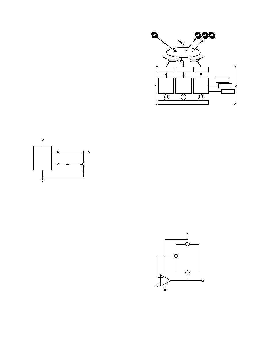
Reference for Converters in Optical Network Control Circuits
In the upcoming high-capacity all-optical router network, Fig-
ure 4 employs arrays of micro-mirrors to direct and route optical
signals from fiber to fiber, without first converting them to elec-
trical form, which reduces the communication speed. The tiny
micro-mechanical mirrors are positioned so that each is illumi-
nated by a single wavelength that carries unique information and
can be passed to any desired input and output fiber. The mir-
rors are tilted by the dual-axis actuators controlled by precision
ADCs and DACs within the system. Due to the microscopic
movement of the mirrors, not only is the precision of the converters
important, but the noise associated with these controlling con-
verters is also extremely critical, because total noise within
the system can be multiplied by the numbers of converters
employed. As a result, the ADR421 is necessary for this applica-
tion for its exceptional low noise to maintain the stability of
the control loop.
CONTROL
ELECTRONICS
PREAMP
AMPL
AMPL
ADR421
ADR421
ADR421
DAC
DAC
ADC
DSP
MEMS MIRROR
ACTIVATOR
RIGHT
ACTIVATOR
LEFT
GIMBAL + SENSOR
SOURCE FIBER
LASER BEAM
DESTINATION
FIBER
Figure 4. All-Optical Router Network
A Negative Precision Reference without Precision Resistors
In many current-output CMOS DAC applications, where the
output signal voltage must be of the same polarity as the reference
voltage, it is often required to reconfigure a current-switching
DAC into a voltage-switching DAC through the use of a 1.25 V
reference, an op amp, and a pair of resistors. Using a current-
switching DAC directly requires the need for an additional
operational amplifier at the output to reinvert the signal. A
negative voltage reference is then desirable from the point that
an additional operational amplifier is not required for either
reinversion (current-switching mode) or amplification (voltage-
switching mode) of the DAC output voltage. In general, any
positive voltage reference can be converted into a negative volt-
age reference through the use of an operational amplifier and a pair
of matched resistors in an inverting configuration. The disad-
vantage to that approach is that the largest single source of error
in the circuit is the relative matching of the resistors used.
A negative reference can easily be generated by adding a preci-
sion op amp and configured as in Figure 5. V
OUT
is at virtual
ground and therefore the negative reference can be taken directly
from the output of the op amp. The op amp must be dual sup-
ply, low offset, and have rail-to-rail capability if negative supply
voltage is close to the reference output.
V
DD
V
DD
V
REF
V
OUT
V
IN
GND
ADR42x
A1 = OP777, OP193
A1
4
6
2
Figure 5. Negative Reference
REV. 0
ADR420/ADR421
11
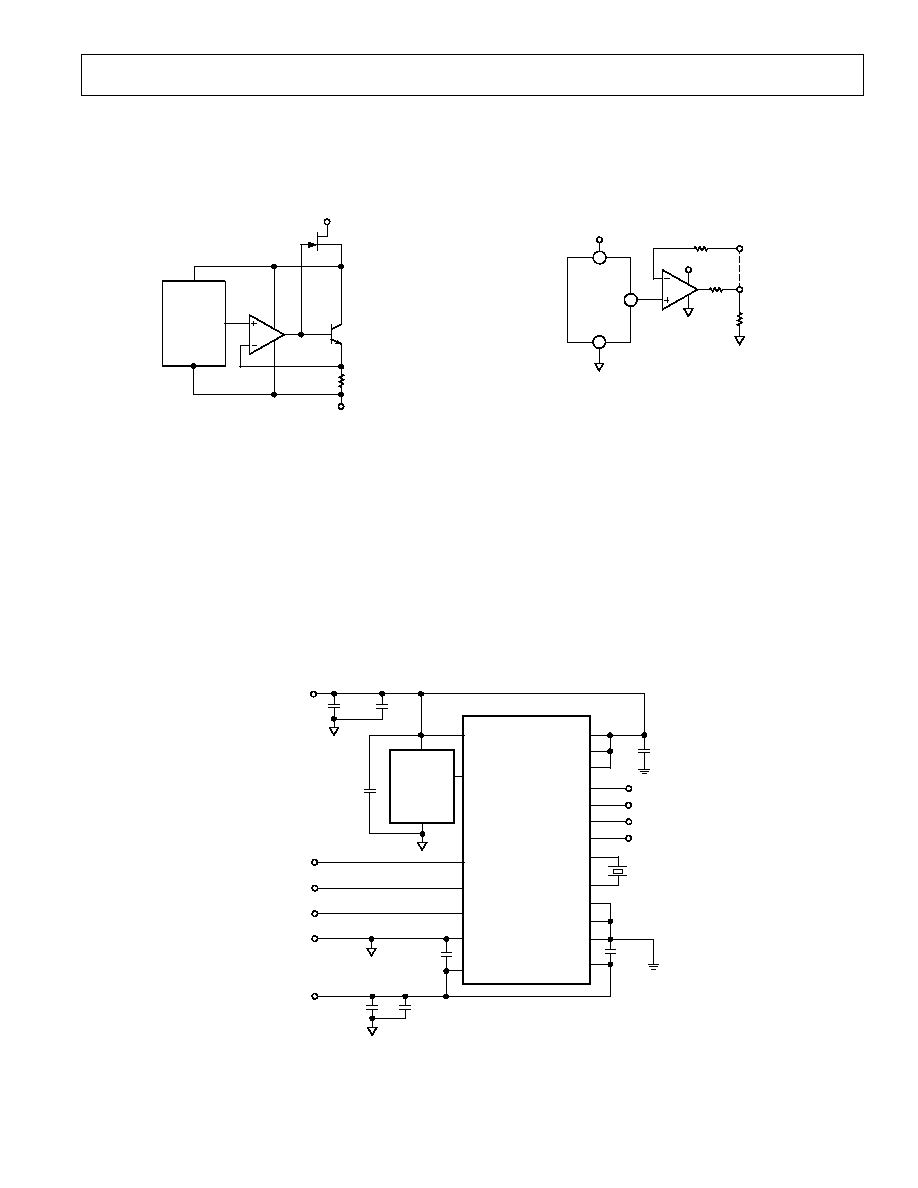
High-Voltage Floating Current Source
The circuit of Figure 6 can be used to generate a floating current
source with minimal self-heating. This particular configuration
can operate on high supply voltages determined by the break-
down voltage of the N-channel JFET.
V
IN
GND
+V
S
ADR42x
R
L
2.10k
OP90
V
S
2N3904
V
OUT
SST111
VISHAY
Figure 6. High-Voltage Floating Current Source
Kelvin Connections
In many portable instrumentation applications, where PC board
cost and area go hand-in-hand, circuit interconnects are very
often of dimensionally minimum width. These narrow lines can
cause large voltage drops if the voltage reference is required to
provide load currents to various functions. In fact, a circuit's
interconnects can exhibit a typical line resistance of 0.45 m
/
square (1 oz. Cu, for example). Force and sense connections,
also referred to as Kelvin connections, offer a convenient method
of eliminating the effects of voltage drops in circuit wires. Load
currents flowing through wiring resistance produce an error
(V
ERROR
= R
× I
L
) at the load. However, the Kelvin connection
of Figure 7 overcomes the problem by including the wiring
resistance within the forcing loop of the op amp. Since the op
amp senses the load voltage, op amp loop control forces the
output to compensate for the wiring error and to produce the
correct voltage at the load.
V
IN
GND
R
LW
ADR42x
V
OUT
FORCE
A1
V
IN
V
OUT
R
LW
R
L
V
OUT
SENSE
A1 = OP191
2
6
4
Figure 7. Advantage of Kelvin Connection
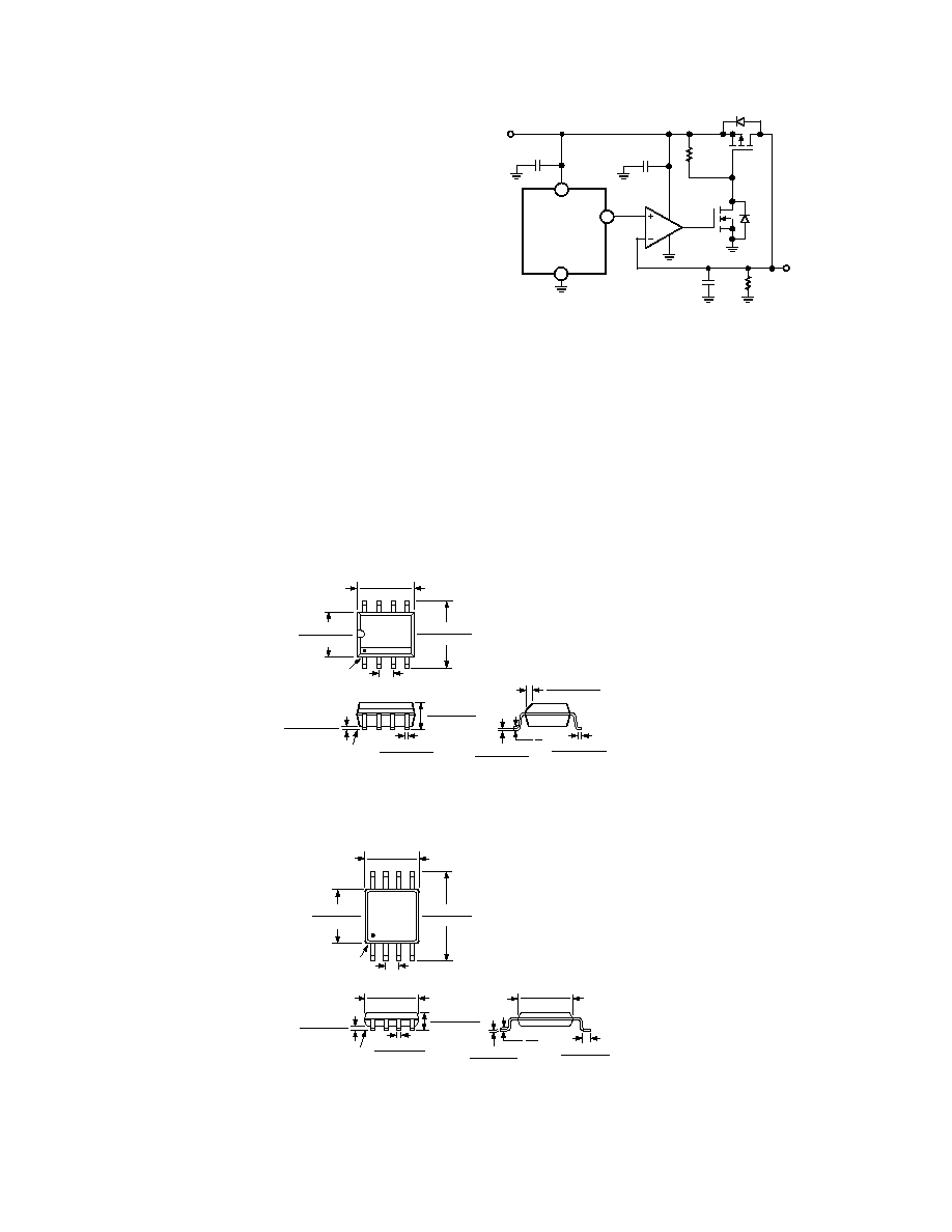
Precision Voltage Reference For Data Converters
The ADR42x family has a number of features that make it ideal
for use with A/D and D/A converters. The exceptional low noise,
tight temperature coefficient, and high accuracy characteristics
make the ADR42x ideal for low noise applications such as cellu-
lar base station applications.
Another example of ADC for which the ADR421 is also well-
suited is the AD7701. Figure 8 shows the ADR421 used as the
precision reference for this converter. The AD7701 is a 16-bit
A/D converter with on-chip digital filtering intended for the
measurement of wide dynamic range and low frequency signals
such as those representing chemical, physical, or biological
processes. It contains a charge-balancing (sigma-delta) ADC,
calibration microcontroller with on-chip static RAM, a clock
oscillator, and a serial communications port.
V
IN
GND
ADR42x
0.1 F
SC1
V
OUT
MODE
CLKOUT
0.1 F
10 F
0.1 F
0.1 F
0.1 F
0.1 F
10 F
AD7701
5V
ANALOG SUPPLY
ANALOG
GROUND
ANALOG
INPUT
CALIBRATE
RANGES
SELECT
AGND
A
IN
AV
SS
CAL
BP/
UP
V
REF
AV
DD
DV
SS
DGND
SC2
CLKIN
SCLK
SDATA
DRDV
CS
SLEEP
DV
DD
DATA READY
READ (TRANSMIT)
SERIAL CLOCK
SERIAL CLOCK
+5V
ANALOG SUPPLY
Figure 8. Voltage Reference for 16-Bit A/D Converter AD7701
12
C024352.54/01(0)
PRINTED IN U.S.A.
ADR420/ADR421
REV. 0
8-Lead Narrow Body SO
(R-8)
0.0098 (0.25)
0.0075 (0.19)
0.0500 (1.27)
0.0160 (0.41)
0.0196 (0.50)
0.0099 (0.25)
45
8
0
0.102 (2.59)
0.094 (2.39)
SEATING
PLANE
0.0098 (0.25)
0.0040 (0.10)
0.0192 (0.49)
0.0138 (0.35)
8
5
4
1
0.1968 (5.00)
0.1890 (4.80)
PIN 1
0.1574 (4.00)
0.1497 (3.80)
0.0500 (1.27)
BSC
0.2440 (6.20)
0.2284 (5.80)
8-Lead Mini_SOIC
(RM-8)
0.011 (0.28)
0.003 (0.08)
0.028 (0.71)
0.016 (0.41)
33
27
0.120 (3.05)
0.112 (2.84)
8
5
4
1
0.122 (3.10)
0.114 (2.90)
0.199 (5.05)
0.187 (4.75)
PIN 1
0.0256 (0.65) BSC
0.122 (3.10)
0.114 (2.90)
SEATING
PLANE
0.006 (0.15)
0.002 (0.05)
0.018 (0.46)
0.008 (0.20)
0.043 (1.09)
0.037 (0.94)
0.120 (3.05)
0.112 (2.84)
OUTLINE DIMENSIONS
Dimensions shown in inches and (mm).
Precision Voltage Regulator
Together with a precision op amp and discrete MOSFETs,
ADR42x can be configured as a precision LDO (Low Dropout
Regulator). The advantages of using such an alternative over
integrated solutions are the 0.05% accuracy and ultralow noise
characteristics, which cannot be achieved with typical LDOs or
switching regulators. Other output voltages are also possible if
adding a pair of precision resistors, one connected between the
drain of M2 and the negative input of the op amp, and another
connected between the negative input of the op amp and
ground. M1 can be any low-cost N-Channel MOSFET. On
the other hand, M2 is a P-Channel MOSFET and is chosen to
handle the amount of load current desired. The choice of R1 is
the trade-off between the current lost through it and the output
turn-off time.
Like most voltage references, ADR42x suffers from low ripple
rejection ratio at high frequency. Therefore, users should
avoid using the output of a switching power supply as the
input of ADR42x.
R
L
5
V
O
2.5V/500mA
C
L
1 F
V
I
C1
0.1 F
C2
0.1 F
V
IN
V
OUT
GND
V+
V
U2
ADR421
U1
R1
100k
M2
M1
U2 = AD820, OP191
M1 = FDV301N, 2N7002
M2 = FDN360P, FDS9430, IRF9530
2
6
4
Figure 9. Voltage Regulator for Portable Equipment