Äîêóìåíòàöèÿ è îïèñàíèÿ www.docs.chipfind.ru
REV. 0
Information furnished by Analog Devices is believed to be accurate and
reliable. However, no responsibility is assumed by Analog Devices for its
use, nor for any infringements of patents or other rights of third parties
which may result from its use. No license is granted by implication or
otherwise under any patent or patent rights of Analog Devices.
a
ADP3810/ADP3811
One Technology Way, P.O. Box 9106, Norwood, MA 02062-9106, U.S.A.
Tel: 617/329-4700
World Wide Web Site: http://www.analog.com
Fax: 617/326-8703
© Analog Devices, Inc., 1996
Secondary Side, Off-Line
Battery Charger Controllers
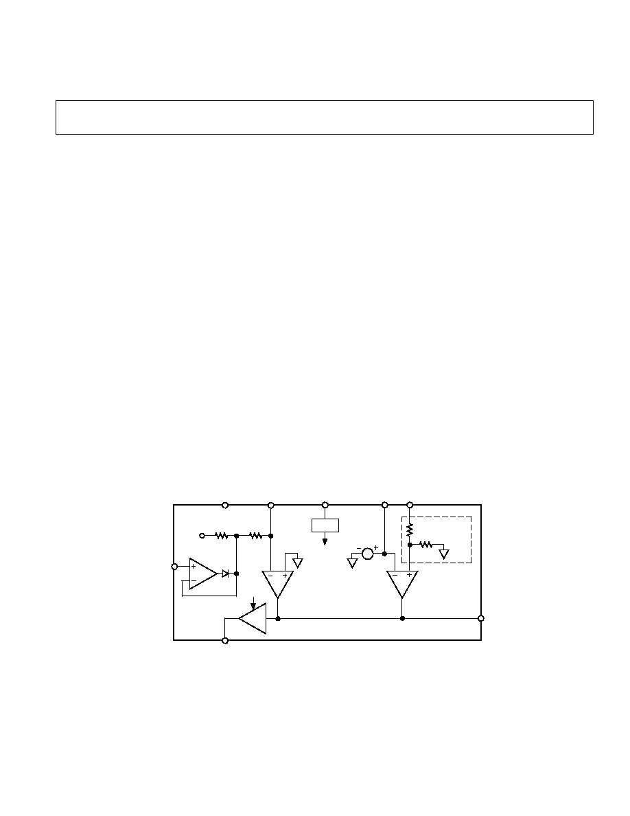
FUNCTIONAL BLOCK DIAGRAM
ADP3810/
ADP3811
V
SENSE
V
CS
COMP
OUT
V
CC
V
REF
GND
V
CTRL
1.5M
80k
V
REF
UVLO
GM
GM1
UVLO
UVLO
R1
R2
ADP3810
ONLY
GM2
V
REF
FEATURES
Programmable Charge Current
High Precision Battery Voltage Limit
Precision 2.000 V Reference
Low Voltage Drop Current Sense: 300 mV Full Scale
Full Operation in Shorted and Open Battery Conditions
Drives Diode-Side of Optocoupler
Wide Operating Supply Range: 2.7 V to 16 V
Undervoltage Lockout
SO-8 Package
ADP3810
Internal Precision Voltage Divider for Battery Sense
Four Final Battery Voltage Options Available: 4.2 V,
8.4 V, 12.6 V, 16.8 V
ADP3811
Adjustable Final Battery Voltage
APPLICATIONS
Battery Charger Controller for:
LiIon Batteries (ADP3810)
NiCad, NiMH Batteries (ADP3811)
GENERAL DESCRIPTION
The ADP3810 and ADP3811 combine a programmable current
limit with a battery voltage limit to provide a constant current,
constant voltage battery charger controller. In secondary side,
off-line applications, the output directly drives the diode side of
an optocoupler to give isolated feedback control of a primary
side PWM. The circuitry includes two gain (g
m
) stages, a preci-
sion 2.0 V reference, a control input buffer, an Undervoltage
Lock Out (UVLO) comparator, an output buffer and an over-
voltage comparator.
The current limit amplifier senses the voltage drop across an
external sense resistor to control the average current for charg-
ing a battery. The voltage drop can be adjusted from 25 mV
to 300 mV, giving a charging current limit from 100 mA to
1.2 amps with a 0.25
sense resistor. An external dc voltage
on the V
CTRL
input sets the voltage drop. Because this input
is high impedance, a filtered PWM output can be used to set
the voltage.
As the battery voltage approaches its voltage limit, the voltage
sense amplifier takes over to maintain a constant battery volt-
age. The two amplifiers essentially operate in an "OR" fash-
ion. Either the current is limited, or the voltage is limited.
The ADP3810 has internal thin-film resistors that are trimmed
to provide a precise final voltage for LiIon batteries. Four volt-
age options are available, corresponding to 1-4 LiIon cells as
follows: 4.2 V, 8.4 V, 12.6 V and 16.8 V.
The ADP3811 omits these resistors allowing any battery volt-
age to be programmed with external resistors.

ADP3810/ADP3811SPECIFICATIONS
2
REV. 0
(40 C
T
A
+85 C, V
CC
= 10.0 V, unless otherwise noted)
ADP3810
Parameter
Conditions
Symbol
Min
Typ
Max
Units
CURRENT SENSE
1
Full-Scale Current Sense Voltage
V
CTRL
= 1.2 V
315
300
285
mV
Minimum Current Sense Voltage
0.0 V
V
CTRL
0.1 V
32
25
18
mV
Current Programming Input Range
V
CTRL
0.0
1.2
V
Gain (V
OUT
/V
CS
)
R
L
= 1 k
A
VCS
74
86
dB
Control Input Bias Current
V
CTRL
Pin
I
BCTRL
10
40
nA
VOLTAGE SENSE
Accuracy
2
--ADP3810
1.0
+1.0
%
Input Resistance--ADP3810
4.2 V Option
R
IN
210k
Input Resistance--ADP3810
8.4 V Option
R
IN
420k
Input Resistance--ADP3810
12.6 V Option
R
IN
630k
Input Resistance--ADP3810
16.8 V Option
R
IN
840k
Offset Voltage--ADP3811
V
OS
2.5
+2.5
mV
Bias Current--ADP3811
I
B
1
10
nA
Gain (V
OUT
/V
SENSE
)
3
R
L
= 1 k
A
VBAT
60
74
dB
REFERENCE
Output Voltage
C
L
= 0.1
µ
F
4
V
REF
2.000
V
Accuracy
ADP3810
1.0
+1.0
%
ADP3811
1.8
+1.8
%
Load Regulation
I
LOAD
= 0 mA to 5 mA
0.25
+0.25
%
Line Regulation
V
CC
= 2.7 V to 16 V
0.004
0.02
%/V
Output Voltage Noise
0.1 Hz to 10 Hz
e
N
35
µ
V p-p
Load Current (Sourcing)
I
L
5
10
mA
OUTPUT
Output Current
V
CC
= 2.7 V
I
OUT
4
6
mA
Saturation Voltage
I
OUT
= 4 mA, V
CC
V
OUT
V
SAT
0.1
0.4
V
Gain (V
OUT
/V
COMP
)
R
L
= 1 k
A
VOUT
6
V/V
UNDERVOLTAGE LOCKOUT
Trip Point-On
2.65
2.7
V
Trip Point-Off
2.5
2.6
V
POWER SUPPLY
Operating Range
2.7
16
V
Quiescent Current
V
CC
2.7 V
I
Q
1.5
3
mA
Turn-Off Current
V
CC
2.5 V
0.5
1
mA
OVERVOLTAGE COMPARATOR
Threshold
ADP3810
Percent Above Full Scale
5
V
OV
%
6
%
ADP3811
Percent Above Full Scale
5
V
OV
%
6
%
Response Time
I
OUT
from 0 mA to 2 mA
t
r
8
µ
s
NOTES
1
20 k
resistor from current sense voltage to V
CS
pin.
2
Applies to 4.2 V, 8.4 V, 12.6 V and 16.8 V options. Includes all error from offset voltage, bias current, resistor divider and voltage reference.
3
Does not include attenuation of input resistor divider for ADP3810.
4
0.1
µ
F load capacitor required for reference operation.
5
Full scale is the programmed final battery voltage: 4.2 V, 8.4 V, 12.6 V or 16.8 V for the ADP3810 or 2.0 V at V
SENSE
for the ADP3811.
All limits at temperature extremes are guaranteed via correlation using standard Statistical Quality Control (SQC) methods.
Specifications subject to change without notice.
ADP3810/ADP3811
3
REV. 0
ABSOLUTE MAXIMUM RATINGS
Supply Voltage, V
CC
. . . . . . . . . . . . . . . . . . . 0.4 V to 18 V
V
CTRL
, V
CS
Input Range . . . . . . . . . . . . . . . . . . 0.4 V to V
CC
V
SENSE
Input Range (ADP3811) . . . . . . . . . . . . 0.4 V to V
CC
V
SENSE
Input Range (ADP3810) . . . . . . . . . . . 0.4 V to 20 V
Maximum Power Dissipation . . . . . . . . . . . . . . . . . . 500 mW
Operating Temperature Range . . . . . . . . . . . 40
°
C to +85
°
C
Storage Temperature Range . . . . . . . . . . . . . 65
°
C to 150
°
C
Lead Temperature (Soldering, 10 sec) . . . . . . . . . . . . +300
°
C
ORDERING GUIDE
Temperature
Package
Battery
Model
Range
Option
Voltage
ADP3810AR-4.2
40
°
C to +85
°
C
SO-8
4.2 V
ADP3810AR-8.4
40
°
C to +85
°
C
SO-8
8.4 V
ADP3810AR-12.6
40
°
C to +85
°
C
SO-8
12.6 V
ADP3810AR-16.8
40
°
C to +85
°
C
SO-8
16.8 V
ADP3811AR
40
°
C to +85
°
C
SO-8
Adjustable
WARNING!
ESD SENSITIVE DEVICE
CAUTION
ESD (electrostatic discharge) sensitive device. Electrostatic charges as high as 4000 V readily
accumulate on the human body and test equipment and can discharge without detection.
Although the ADP3810/ADP3811 features proprietary ESD protection circuitry, permanent
damage may occur on devices subjected to high energy electrostatic discharges. Therefore, proper
ESD precautions are recommended to avoid performance degradation or loss of functionality.
PIN DESCRIPTION
Mnemonic Function
V
SENSE
Battery Voltage Sense Input.
V
CS
Current Sense Input.
V
REF
Reference Output. Nominally 2.0 V.
COMP
External Compensation Pin.
OUT
Optocoupler Current Output Drive.
V
CTRL
DC Control Input to Set Current Limit, 0 V to 1.2 V.
V
CC
Positive Supply.
GND
Ground Pin.
PIN CONFIGURATION
1
2
3
4
8
7
6
5
TOP VIEW
(Not to Scale)
ADP3810
ADP3811
V
SENSE
V
CS
COMP
OUT
V
CC
V
REF
GND
V
CTRL
ADP3810/
ADP3811
V
SENSE
V
CS
COMP
OUT
V
CC
V
REF
V
CTRL
1.5M
80k
V
REF
GM1
UVLO
UVLO
R1
ADP3810
ONLY
GM2
V
REF
100µA
R2
R1
ADP3811
ONLY
R2
0.1µF
2.0V
0.1µF
200
1.2V
GM3
R3
BATTERY
V
BAT
V
RCS
R
CS
GND
I
OUT
V
IN
RETURN
C
C
R
C
I
CHARGE
DC/DC
CONVERTER
GND
OUT
IN
CTRL
UVLO
BUFFER
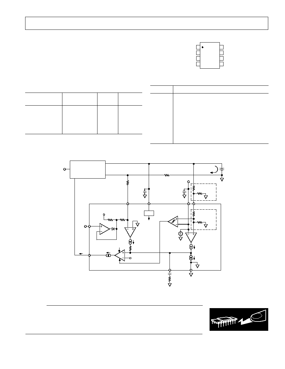
Figure 1. Simplified Battery Charger
ADP3810/ADP3811
4
REV. 0
TEMPERATURE
°
C
REFERENCE VOLTAGE Volts
2.002
1.994
50
25
100
0
25
50
75
2.000
1.998
1.996
2.004
2 TYPICAL PARTS
V
CC
= +10V
I
L
= 100µA
C
L
= 0.1µF
Figure 2. Reference Output Voltage
vs. Temperature for Two Typical Parts
FREQUENCY Hz
PSRR dB
20
30
80
100
1k
1M
10k
100k
50
60
70
40
V
CC
= +10V
I
L
= 100µA
C
L
= 0.1µF
Figure 5. Reference PSRR vs.
Frequency
TEMPERATURE
°
C
CURRENT SENSE VOLTAGE mV
294
296
304
50
25
100
0
25
50
75
298
300
302
V
CC
= +10V
R3 = 20k
Figure 8. Full-Scale Current Sense
Voltage vs. Temperature
LOAD CURRENT mA
DROPOUT VOLTAGE mV
250
200
0
0
3
18
6
9
12
15
150
100
50
V
CC
= +10V
C
L
= 0.1µF
Figure 3. Reference Drop-Out Volt
age (V
CC
V
REF
) vs. Load Current
FREQUENCY Hz
REFERENCE NOISE DENSITY nV/
Hz
3000
2500
0
1
10
10k
100
1k
1500
1000
500
2000
V
CC
= +10V
I
L
= 100µA
C
L
= 0.1µF
Figure 6. Reference Noise Density
vs. Frequency
SUPPLY VOLTAGE, V
CC
Volts
CURRENT SENSE VOLTAGE mV
294
296
304
2
4
16
6
8
10
12
14
298
300
302
V
CC
= +10V
R3 = 20k
Figure 9. Full-Scale Current Sense
Voltage vs. V
CC
TEMPERATURE
°
C
REFERENCE DROPOUT VOLTAGE Volts
0.12
0.04
50
25
100
0
25
50
75
0.10
0.08
0.06
0.14
V
CC
= +10V
I
L
= 5mA
C
L
= 0.1µF
Figure 4. Reference Dropout Voltage
vs. Temperature
CONTROL VOLTAGE, V
CTRL
Volts
CHARGE CURRENT Amps
1.6
1.4
0
0
0.2
1.4
0.4
0.6
0.8
1.0
1.2
1.0
0.2
0.8
0.6
0.4
1.2
R
CS
= 0.25
R3 = 20k
Figure 7. Charge Current vs. Control
Voltage
FREQUENCY Hz
OPEN-LOOP GAIN dB
100
80
60
40
20
40
60
20
0
10
1M
10k
0
225
135
180
45
90
100
1k
C
COMP
= 0.01µF
T
A
= +25
°
C
V
CC
= +10V
100k
PHASE SHIFT Degrees
GAIN
PHASE
Figure 10. GM1 Open-Loop Gain and
Phase vs. Frequency
Typical Performance Characteristics
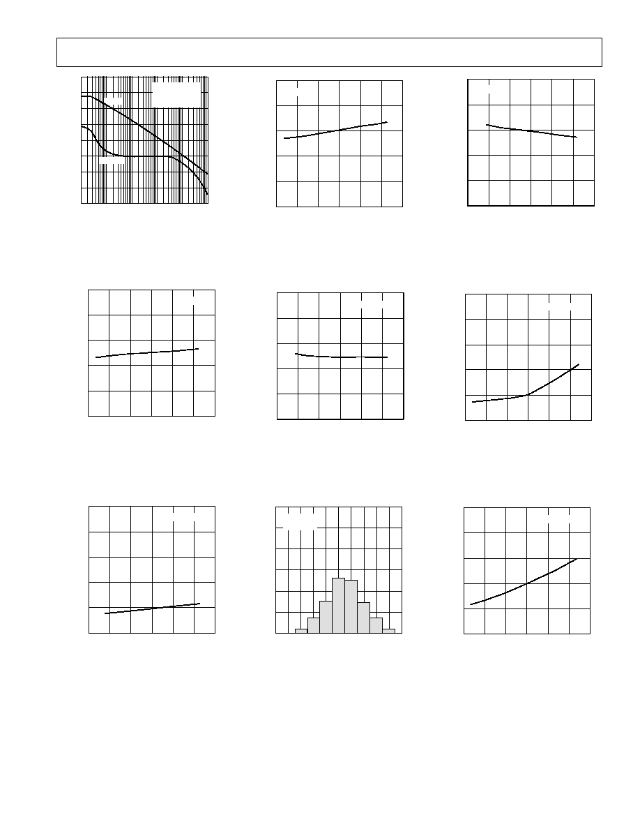
ADP3810/ADP3811
5
REV. 0
FREQUENCY Hz
OPEN-LOOP GAIN dB
100
80
60
40
20
40
60
20
0
10
1M
10k
0
225
135
180
45
90
100
1k
C
COMP
= 0.01µF
T
A
= +25
°
C
V
CC
= +10V
100k
PHASE SHIFT Degrees
GAIN
PHASE
Figure 11. GM2 Open-Loop Gain and
Phase vs. Frequency
TEMPERATURE
°
C
GM2 OFFSET mV
1.0
0.5
1.5
50
25
100
0
25
50
75
0
0.5
1.0
V
CC
= +10V
Figure 14. ADP3811 GM2 Offset vs.
Temperature
SUPPLY VOLTAGE, V
CC
Volts
V
SENSE
BIAS CURRENT nA
2.5
2.0
0
0
3
18
6
9
12
15
1.5
1.0
0.5
T
A
= +25
°
C
Figure 17. ADP3811 V
SENSE
Bias
Current vs. V
CC
TEMPERATURE
°
C
VOLTAGE SENSE ACCURACY %
1.0
0.5
1.5
50
25
100
0
25
50
75
0
0.5
1.0
V
CC
= +10V
Figure 12. ADP3810 Voltage Sense
Accuracy vs. Temperature
SUPPLY VOLTAGE, V
CC
Volts
GM2 OFFSET mV
1.0
0.5
1.5
0
3
18
6
9
12
15
0
0.5
1.0
T
A
= +25
°
C
Figure 15. ADP3811, GM2 Offset
vs. V
CC
V
OV%
%
QUANTITY Parts
120
60
0
5.0 5.2 5.4 5.6 5.8 6.0 6.2 6.4 6.6 6.8 7.0
100
80
40
20
V
CC
= +10V
T
A
= +25
°
C
Figure 18. Overvoltage Comparator
Distribution (V
OV%
)
SUPPLY VOLTAGE, V
CC
Volts
1.0
0.5
1.5
0
3
18
6
9
12
15
0
0.5
1.0
VOLTAGE SENSE ACCURACY %
T
A
= +25
°
C
Figure 13. ADP3810 Voltage Sense
Accuracy vs. V
CC
TEMPERATURE
°
C
V
SENSE
BIAS CURRENT nA
2.5
2.0
0
50
25
100
0
25
50
75
1.5
1.0
0.5
V
CC
= +10V
Figure 16. ADP3811 V
SENSE
Bias
Current vs. Temperature
TEMPERATURE
°
C
V
OV%
%
12
10
2
50
25
100
0
25
50
75
8
6
4
V
CC
= +10V
Figure 19. Overvoltage Comparator
Threshold (V
OV%)
vs. Temperature
ADP3810/ADP3811
6
REV. 0
OUTPUT GAIN (V
OUT
/V
COMP
) V/V
QUANTITY Parts
240
120
0
5.0 5.2 5.4 5.6 5.8 6.0 6.2 6.4 6.6 6.8 7.0
200
160
80
40
V
CC
= +10V
T
A
= +25
°
C
R
L
= 1k
Figure 20. Output Gain (V
OUT
/V
COMP
)
Distribution
APPLICATIONS SECTION
Functional Description
The ADP3810 and ADP3811 are designed for charging NiCad,
NiMH and LiIon batteries. Both parts provide accurate voltage
sense and current sense circuitry to control the charge current
and final battery voltage. Figure 1 shows a simplified battery
charging circuit with the ADP3810/ADP3811 controlling an
external dc-dc converter. The converter can be one of many
different types such as a Buck converter, Flyback converter or a
linear regulator. In all cases, the ADP3810/ADP3811 maintains
accurate control of the current and voltage loops, enabling the
use of a low cost, industry standard dc-dc converter without
compromising system performance. Detailed realizations of
complete circuits including the dc-dc converter are included
later in this data sheet.
The ADP3810 and ADP3811 contain the following blocks
(shown in Figure 1):
· Two "GM" type error amplifiers control the current loop
(GM1) and the voltage loop (GM2).
· A common COMP node is shared by both GM amplifiers
such that an RC network at this node helps compensate both
control loops.
· A precision 2.0 V reference is used internally and is available
externally for use by other circuitry. The 0.1
µ
F bypass ca-
pacitor shown is required for stability.
· A current limited buffer stage (GM3) provides a current out-
put, I
OUT
, to control an external dc-dc converter. This out-
put can directly drive an optocoupler in isolated converter
applications. The dc-dc converter must have a control scheme
such that higher I
OUT
results in lower duty cycle. If this is
not the case, a simple, single transistor inverter can be used
for control phase inversion.
· An amplifier buffers the charge current programming volt-
age, V
CTRL
, to provide a high impedance input.
· An UVLO circuit shuts down the GM amplifiers and the
output when the supply voltage (V
CC
) falls below 2.7 V. This
protects the charging system from indeterminate operation.
· A transient overshoot comparator quickly increases I
OUT
when the voltage on the "+" input of GM2 rises over 120 mV
above V
REF
. This clamp shuts down the dc-dc converter to
quickly recover from overvoltage transients and protect ex-
ternal circuitry.
Description of Battery Charging Operation
The IC based system shown in Figure 1 charges a battery with a
dc current supplied by a dc-dc converter, which is most likely a
switching type supply but could also be a linear supply where
feasible. The value of the charge current is controlled by the
feedback loop comprised of R
CS
, R3, GM1, the external dc-dc
converter and a dc voltage at the V
CTRL
input. The actual
charge current is set by the voltage, V
CTRL
, and is dependent
upon the choice for the values of R
CS
and R3 according to the
formula below:
I
CHARGE
=
1
R
CS
×
R3
80 k
×
V
CTRL
Typical values are R
CS
= 0.25
and R3 = 20 k
, which result
in a charge current of 1.0 A for a control voltage of 1.0 V. The
80 k
resistor is internal to the IC, and it is trimmed to its ab-
solute value. The positive input of GM1 is referenced to
ground, forcing the V
CS
pin to a virtual ground.
The resistor R
CS
converts the charge current into the voltage at
V
RCS
, and it is this voltage that GM1 is regulating. The voltage
at V
RCS
is equal to (R3/80 k
) V
CTRL
. When V
CTRL
equals
1.0 V, V
RCS
equals 250 mV. If V
RCS
falls below its pro-
grammed level (i.e., the charge current increases), the negative
input of GM1 goes slightly below ground. This causes the out-
put of GM1 to source more current and drive the COMP node
high, which forces the current, I
OUT
, to increase. A higher I
OUT
decreases the drive to the dc-dc converter, reducing the charg-
ing current and balancing the feedback loop.
As the battery approaches its final charge voltage, the voltage
loop takes over. The system becomes a voltage source, floating
the battery at constant voltage thereby preventing overcharging.
The constant voltage feature also protects the circuitry that is
actually powered by the battery from overvoltage if the battery is
removed. The voltage loop is comprised of R1, R2, GM2 and
the dc-dc converter. The final battery voltage is simply set by
the ratio of R1 and R2 according to the following equation
(V
REF
= 2.000 V):
V
BAT
=
2.000V
×
R1
R2
+
1
If the battery voltage rises above its programmed voltage,
V
SENSE
is pulled above V
REF
. This causes GM2 to source more
current, raising the COMP node voltage and I
OUT
. As with the
V
CC
Volts
V
OUT
/V
COMP
V/V
8
7
3
0
3
18
6
9
12
15
6
5
4
R
L
= 1k
V
OUT
= +1.0V
T
A
= 40
°
C
T
A
= +25
°
C
T
A
= +85
°
C
Figure 21. Output Gain (V
OUT
/V
COMP
)
vs. V
CC
TEMPERATURE
°
C
0.25
0.20
0
50
25
100
0
25
50
75
0.15
0.10
0.05
OUTPUT SATURATION
VOLTAGE, V
SAT
Volts
V
CC
= +10V
I
LOAD
= 5mA
Figure 22. V
SAT
vs. Temperature

ADP3810/ADP3811
7
REV. 0
current loop, the higher I
OUT
reduces the duty cycle of the dc-dc
converter and causes the battery voltage to fall, balancing the
feedback loop.
Each GM stage is designed to be asymmetrical so that each am-
plifier can only source current. The outputs are tied together at
the COMP node and loaded with an internal constant current
sink of approximately 100
µ
A. Whichever amplifier sources
more current controls the voltage at the COMP node and there-
fore controls the feedback. This scheme is a realization of an
analog "OR" function where GM1 or GM2 has control of the
dc-dc converter and the charging circuitry. Whenever the cir-
cuit is in full current limiting or full voltage limiting, the respec-
tive GM stage sources an identical amount of current to the
fixed current sink. The other GM stage sources zero current
and is out of the loop. In the transition region, both GM stages
source some of the current to comprise the full amount of the
current sink. The high gains of GM1 and GM2 ensure a
smooth but sharp transition from current control to voltage con-
trol. Figure 24 shows a graph of the transition from current to
voltage mode, that was measured on the circuit in Figure 23 as
detailed below. Notice that the current stays at its full pro-
grammed level until the battery is within 200 mV of the final pro-
grammed voltage (10 V in this case), which maintains fast
charging through almost all of the battery voltage range. This
improves the speed of charging compared to a scheme that re-
duces the current at lower battery voltages.
The second element in a battery charging system is some form
of a dc-dc converter. To achieve high efficiency, the dc-dc con-
verter can be an isolated off-line switching power supply, or it
can be an isolated or nonisolated Buck or other type of switch-
ing power supply. For lower efficiency requirements, a linear
regulator fed from a wall adapter can be used. In the above dis-
cussion, the current, I
OUT
, controls the duty cycle of a switching
supply; but in the case of the linear regulator, I
OUT
controls the
pass transistor drive. Examples of these topologies are shown
later in this data sheet. If an off-line supply such as a flyback
converter is used, and isolation between the control logic and
the ADP3810/ADP3811 is required, an optocoupler can be in-
serted between the ADP3810/ADP3811 output and the control
input of the primary side PWM.
Charge Termination
If the system is charging a LiIon battery, the main criteria to de-
termine charge termination is the absolute battery voltage. The
ADP3810, with its accurate reference and internal resistors, ac-
complishes this task. The ADP3810's guaranteed accuracy
specification of
±
1% of the final battery voltage ensures that a
LiIon battery will not be overcharged. This is especially impor-
tant with LiIon batteries because overcharging can lead to cata-
strophic failure. It is also important to insure that the battery be
charged to a voltage equal to its optimal final voltage (typically
4.2 V per cell). Stopping at less than 1% of full-scale results in
a battery that has not been charged to its full mAh capacity,
reducing the battery's run time and the end equipment's operat-
ing time.
The ADP3810/ADP3811 does not include circuitry to detect
charge termination criteria such as
V/
t or
T/
t, which are
common for NiCad and NiMH batteries. If such charge termi-
nation schemes are required, a low cost microcontroller can be
added to the system to monitor the battery voltage and tempera-
ture. A PWM output from the microcontroller can subsequently
program the V
CTRL
input to set the charge current. The high
impedance of V
CTRL
enables the inclusion of an RC filter to in-
tegrate a PWM output into a dc control voltage.
Compensation
The voltage and current loops have significantly different natu-
ral and crossover frequencies in a battery charger application, so
the two loops most likely need different pole/zero feedback com-
pensation. Figure 1 shows a single RC network from the
COMP node to ground. This is primarily for low frequency
compensation (f
C
< 100 Hz) of the voltage loop. Since the
COMP node is shared by both GM stages, this compensation
also affects the current loop. The internal 200
resistor does
change the zero location of the compensation for the current
loop with respect to the voltage loop. To provide a separate
higher frequency compensation (f
C
~ 1 kHz10 kHz), a second
series RC may be needed. A detailed calculation of the com-
pensation values is given later in this data sheet.
ADP3810 and ADP3811 Differences
The main difference between the ADP3810 and the ADP3811
is illustrated in Figure 1. The resistors R1 and R2 are external
for the ADP3811 and internal for the ADP3810. The ADP3810
is specifically designed for LiIon battery charging, and thus, the
internal resistors are precision thin-film resistors laser trimmed
for LiIon cell voltages. Four different final voltage options are
available in the ADP3810: 4.2 V, 8.4 V, 12.6 V, and 16.8 V.
For slightly different voltages to accommodate different LiIon
chemistries, please contact the factory. The ADP3811 does not in-
clude the internal resistors, allowing the designer to choose any
final battery voltage by appropriately selecting the external resis-
tors. Because the ADP3810 is specifically for LiIon batteries,
the reference is trimmed to a tighter accuracy specification of
±
1% instead of
±
2% for the ADP3811.
V
CTRL
Input and Charge Current Programming Range
The voltage on the V
CTRL
input determines the charge current
level. This input is buffered by an internal single supply ampli-
fier (labeled BUFFER) to allow easy programmability of V
CTRL
.
For example, for a fixed charge current, V
CTRL
can be set by a
resistor divider from the reference output. If a microcontroller
is setting the charge current, a simple RC filter on V
CTRL
enables
the voltage to be set by a PWM output from the micro. Of
course, a digital-to-analog converter could also be used, but the
high impedance input makes a PWM output the economical
choice. The bias current of V
CTRL
is typically 25 nA, which
flows out of the pin.
The guaranteed input voltage range of the buffer is from 0.0 V
to 1.2 V. When V
CTRL
is in the range of 0.0 V to 0.1 V, the out-
put of the internal amplifier is fixed at 0.1 V. This corresponds
to a charge current of 100 mA for R
CS
= 0.25
, R3 = 20 k
.
The graph of charge current versus V
CTRL
in Figure 7 shows this
relationship. Figure 1 shows a diode in series with the buffer's
output and a 1.5 M
resistor from V
REF
to this output. The
diode prevents the amplifier from sinking current, so for small
input voltages the buffer has an open output. The 1.5 M
resistor forms a divider with the internal 80 k
resistor to fix the
output at 0.1 V, i.e., about 10% of the maximum current. This
corresponds to the typical trickle charge current level for NiCad
batteries. When V
CTRL
rises above 0.1 V, the buffer sources
current and the output follows the input. The total range of
V
CTRL
from 0.0 V. to 1.2 V results in a charge current range
from 100 mA to 1.2 A (for R
CS
= 0.25
, R3 = 20 k
). Larger

ADP3810/ADP3811
8
REV. 0
charge current levels can be obtained by either reducing the
value of R
CS
or increasing the value of R3. The main penalty of
increasing R3 is lower efficiency due to the larger voltage drop
across R
CS
, and the penalty of decreasing R
CS
is lower accuracy
(but higher efficiency) as discussed below.
V
REF
Output
The internal band gap reference is not only used internally for
the voltage and current loops, but it is also available externally if
an accurate voltage is needed. The reference employs a pnp
output transistor for low dropout operation. Figure 3 shows a
typical graph of dropout voltage versus load current. The refer-
ence is guaranteed to source 5 mA with a dropout voltage of
400 mV or less. The 0.1
µ
F capacitor on the reference pin is in-
tegral in the compensation of the reference and is therefore re-
quired for stable operation. If desired, a larger value of capacitance
can also be used for the application, but a smaller value should
not be used. This capacitor should be located close to the V
REF
pin. Additional reference performance graphs are shown in Fig-
ures 2 through 6.
Output Stage
The output stage performs two important functions. It is a
buffer for the compensation node, and as such, it has a high im-
pedance input. It is also a GM stage. The OUT pin is a current
output to enable the direct drive of an optocoupler for isolated
applications. The gain from the COMP node to the OUT pin is
approximately 5 mA/V. With a load resistor of 1 k
, the voltage
gain is equal to five as specified in the data sheet. A different
load resistor results in a gain equal to R
L
×
(5 mA/V). Figures
20 and 21 show how the gain varies from part to part and versus
the supply voltage, respectively. The guaranteed output current
is 5 mA, which is much more than the typical 1 mA to 2 mA re-
quired in most applications.
Current Loop Accuracy Considerations
The accuracy of the current loop is dependent on several factors
such as the offset of GM1, the offset of the V
CTRL
buffer, the ra-
tio of the internal 80 k
compared to the external 20 k
resis-
tor, and the accuracy of R
CS
. The specification for current loop
accuracy states that the full-scale current sense voltage, V
RCS
, of
300 mV is guaranteed to be within 15 mV of this value. This
assumes an exact 20 k
resistor for R3. Any errors in this resis-
tor will result in further errors in the charge current value. For
example, a 5% error in resistor value will add a 5% error to the
charge current. The same is true for R
CS
, the current sense resis-
tor. Thus, 1% or better resistors are recommended.
As mentioned above, decreasing the value of R
CS
increases the
charge current. Since it is V
RCS
that is specified, the actual
value of R
CS
is not accounted for in the specification. An example
where R
CS
= 0.1
illustrates its impact on the accuracy of the
charge current. The range of V
RCS
is from 25 mV
±
5 mV to
300 mV
±
15 mV. This results in a charge current range from
250 mA
±
50 mA to 3 A
±
150 mA, as opposed to a charge cur-
rent range of 100 mA
±
20 mA to 1.2 A
±
60 mA for R
CS
=
0.25
. Thus, not only is the minimum current changed, but
the absolute variation around the set point is increased (although
the percentage variation is the same).
Voltage Loop Accuracy Considerations
The accuracy of the voltage loop is dependent on the offset of
GM2, the accuracy of the reference voltage, the bias current of
GM2 through R1 and R2, and the ratio of R1/R2. For the de-
manding application of charging LiIon batteries, the accuracy of
the ADP3810 is specified with respect to the final battery volt-
age. This is tested in a full feedback loop so that the single ac-
curacy specification given in the specification table accounts for
all of the errors mentioned above. For the ADP3811, the resis-
tors are external, so the final voltage accuracy needs to be deter-
mined by the designer. Certainly, the tolerance of the resistors
has a large impact on the final voltage accuracy, and 1% or bet-
ter is recommended.
Supply Range
The supply range is specified from 2.7 V to 16 V. However, a
final battery voltage option for the ADP3810 is 16.8 V. The
16.8 V is divided down by the thin film resistors to 2.0 V inter-
nally. Thus, the input to GM2 never sees much more than 2.0 V,
which is well below the V
CC
voltage limit. In fact, V
CC
can be
fixed to 2.7 V and the ADP3810 will still control the charging of
a 16.8 V battery stack. The ADP3811, with external resistors,
can charge batteries to voltages well in excess of its supply volt-
age. However, if the final battery voltage is above 16 V, V
CC
cannot be supplied directly from the battery as it is in Figure 1.
Alternative circuits must be employed as will be discussed later.
Decoupling capacitors should be located close to the supply pin.
The actual value of the capacitors depends on the application,
but at the very least a 0.1
µ
F capacitor should be used.
OFF-LINE, ISOLATED, FLYBACK BATTERY CHARGER
The ADP3810 and ADP3811 are ideal for use in isolated charg-
ers. Because the output stage can directly drive an optocoupler,
feedback of the control signal across an isolation barrier is a
simple task. Figure 23 shows a complete flyback battery charger
with isolation provided by the flyback transformer and the
optocoupler. The essential operation of the circuit is not much
different from the simplified circuit described in Figure 1. The
GM1 loop controls the charge current, and the GM2 loop con-
trols the final battery voltage. The dc-dc converter block is
comprised of a primary side PWM circuit and flyback trans-
former, and the control signal passes through the optocoupler.
The circuit in Figure 23 incorporates all of the features neces-
sary to assure long battery life with rapid charging capability.
By using the ADP3810 for charging LiIon batteries, or the
ADP3811 for NiCad and NiMH batteries, component count is
minimized, reducing system cost and complexity. With the cir-
cuit as presented or with its many possible variations, designers
no longer need to compromise charging performance and bat-
tery life to achieve a cost effective system.
Primary Side Considerations
A typical current-mode flyback PWM controller was chosen for
the primary control circuit for several reasons. First and most
importantly, it is capable of operating from very small duty
cycles to near the maximum designed duty cycle. This makes it
a good choice for a wide input ac supply voltage variation re-
quirement, which is usually between 70 V270 V ac for world
wide applications. Add to that the additional requirement of
0% to 100% current control, and the PWM duty cycle must
have a wide range. This charger achieves these ranges while
maintaining stable feedback loops.
The detailed operation and design of the primary side PWM is
widely described in the technical literature and is not detailed
here. However, the following explanation should make clear the
reasons for the primary side component choices. The PWM fre-
quency is set to around 100 kHz as a reasonable compromise
ADP3810/ADP3811
9
REV. 0
between inductive and capacitive component sizes, switching
losses and cost.
The primary PWM-IC circuit derives its starting V
CC
through a
100 k
resistor directly from the rectified ac input. After start-
up, a conventional bootstrapped sourcing circuit from an auxil-
iary flyback winding wouldn't work, since the flyback voltage
would be reduced below the minimum V
CC
level specified for
the 3845 under a shorted or discharged battery condition. There-
fore, a voltage doubler circuit was developed (as shown in Fig-
ure 23) that provides the minimum required V
CC
for the IC
across the specified ac voltage range even with a shorted battery.
While the signal from the ADP3810/ADP3811 controls the av-
erage charge current, the primary side should have a cycle by
cycle limit of the switching current. This current limit has to be
designed so that, with a failed or malfunctioning secondary cir-
cuit or optocoupler, the primary power circuit components (the
FET and transformer) won't be overstressed. In addition, dur-
ing start-up or for a shorted battery, V
CC
to the ADP3810/
ADP3811 won't be present. Thus, the primary side current
limit is the only control of the charge current. As the secondary
side V
CC
rises above 2.7 V, the ADP3810/ADP3811 takes over
and controls the average current. The primary side current limit
is set by the 1.6
current sense resistor connected between the
power NMOS transistor, IRFBC30, and ground.
The current drive of the ADP3810/ADP3811's output stage di-
rectly connects to the photodiode of an optocoupler with no ad-
ditional circuitry. With 5 mA of output current, the output stage
can drive a variety of optocouplers. An MOC8103 is shown as
an example. The current of the photo-transistor flows through
the 3.3 k
feedback resistor, R
FB
, setting the voltage at the
3845's COMP pin, thus controlling the PWM duty cycle. The
controlled switching regulator should be designed as shown so
that more LED current from the optocoupler reduces the duty
cycle of the converter. Approximately 1 mA should be the
9.1
3W
1A
L
N
AC
120/220V
22nF
1N4148
13V
330pF 330
10k
10
1k
1.6
470pF
47µF
C
F
1nF
R
F
3.3k
3.3k
100k
IRFBC30
50µF/450V
TX1**
10nF
1N4148 100
22µF
C
F1
1mF
R3
20k
*
MURD320
R
CS
0.25
*
C
C2
0.2µF
R
C2
300
R4
1.2k
3.3V
0.1µF
3.3k
2.2nF
OPTO COUPLER
MOC8103
C
F2
220µF
0.1µF
0.1µF
R1
80.6k
*
R2
20k
*
R
C1
10k
C
C1
1µF
V
CS
V
CC
V
REF
V
SENSE
OUT
COMP
GND
V
CTRL
0.1µF
ADP3810/ADP3811
V
OUT
BATTERY
CHARGE
CURRENT
CONTROL
VOLTAGE
MAXIMUM V
OUT
= +10V
CHARGE CURRENT 0.1A TO 1A
* 1% TOLERANCE
** TX1
f = 120kHz
L
PR
= 750µH
L
SEC
= 7.5µH
V
CC
OUTPUT
COMP
V
FB
I
SENSE
V
REF
RT/CT
GND
PWM
3845
Figure 23. ADP3810/ADP3811 Controlling an Off-Line, Flyback Battery Charger
maximum current needed to reduce the duty cycle to zero. The
difference between the 5 mA drive and the 1 mA requirement
leaves ample margin for variations in the optocoupler gain.
Secondary Side Considerations
For the lowest cost, a current-mode flyback converter topology
is used. Only a single diode is needed for rectification
(MURD320 in Figure 23), and no filter inductor is required.
The diode also prevents the battery from back driving the
charger when input power is disconnected. A 1 mF capacitor
filters the transformer current, providing an average dc current
to charge the battery. The resistor, R
CS
, senses the average cur-
rent which is controlled via the V
CS
input. In this case, the
charging current has high ripple due to the flyback architecture,
so a low-pass filter (R3 and C
C2
) on the current sense signal is
needed. This filter has an extra inverted zero due to R
C2
to im-
prove the phase margin of the loop. The 1 mF capacitor is con-
nected between V
OUT
and the 0.25
sense resistor. To provide
additional decoupling to ground, a 220
µ
F capacitor is also con-
nected to V
OUT
. Output ripple voltage is not critical, so the out-
put capacitor was selected for lowest cost instead of lowest
ripple. Most of the ripple current is shunted by the parallel bat-
tery, if connected. If needed, high frequency ringing caused by
circuit parasitics can be damped with a small RC snubber across
the rectifier.
The V
CC
source to the ADP3810/ADP3811 can come from a di-
rect connection to the battery as long as the battery voltage re-
mains below the specified 16 V operating range. If the battery
voltage is less then 2.7 V (e.g., with a shorted battery, or a bat-
tery discharged below it's minimum voltage), the ADP3810/
ADP3811 will be in Undervoltage Lock Out (UVLO) and will
not drive the optocoupler. In this condition, the primary PWM
circuit will run at its designed current limit. The V
CC
of the
ADP3810/ADP3811 can be boosted using the circuit shown in
Figure 23. This circuit keeps V
CC
above 2.7 V as long as the
ADP3810/ADP3811
10
REV. 0
battery voltage is at least 1.5 V with a programmed charge cur-
rent of 0.1 A. For a higher programmed charge current, the
battery voltage can drop below 1.5 V, and V
CC
is still maintained
above 2.7 V. This is because of the additional energy in the
flyback transformer, which transfers more energy through the
10 nF capacitor to V
CC
. The 22
µ
F bypass capacitor on V
CC
stores the energy transferred through the 10 nF capacitor.
Secondary Side Component Calculations
Design Criteria:
Charging a 6 cell NiCad battery.
Max Individual Cell Voltage:
V
CELLMAX
= 1.67 V
Max Battery Stack Voltage:
V
OMAX
= 6
×
1.67 V = 10 V
Max Charge Current:
I
OMAX
= 1 A
Max Control Voltage:
V
CTRL
= 1 V (for I
OMAX
= 1 A)
R
S
Fixed Value:
R
S
= 20 k
Pick a Value for R1:
R1 = 80.6 k
The voltage limit of 10 V is approximately 10% above the maxi-
mum fully charged voltage when
V/
t termination is used.
This limit gives a second level of protection without interfering
with
V/
t charge termination.
Component Value Calculations:
Current Sense Resistor:
R
CS
= V
CTRL
/(4
×
I
OMAX
) = 1/(4
×
1)
= 0.25 W, 1%, 0.5 W
Battery Divider, R2:
R2 = V
REF
×
R1/(V
OMAX
V
REF
)
R2 = 2
×
80.6 k
/(10 V2 V) =
20.15 k
, Pick 20.0 k
The final voltage and charge current accuracy is dependent
upon the resistor tolerances. Choose appropriate tolerances for
the desired accuracy. One percent accuracy is recommended.
Charger Performance Summary
The charger circuit properly executes the charging algorithm ex-
hibiting stable operation regardless of battery conditions, includ-
ing an open circuit load. The circuit can charge to other battery
voltages by modifying only the battery voltage sense divider. As
would be expected, circuit efficiency is best at high battery volt-
ages. Replacing the output blocking rectifier diode with a
Schottky would improve efficiency if the Schottky's leakage
could be tolerated, and its reverse voltage rating met the appli-
cation requirement.
V
OUT
1.0
0.3
0.0
2
11
3
I
LIMIT
4
5
6
7
8
9
10
0.9
0.4
0.2
0.1
0.8
0.6
0.7
0.5
V
CTRL
= 0.125V
V
CTRL
= 0.25V
V
CTRL
= 0.5V
V
CTRL
= 1.0V
Figure 24. Charge Current vs. Battery Voltage at Four Set-
tings for the Flyback Charger in Figure 23
The Battery Charge Current vs. Battery Voltage characteristics
for four different charge current settings are given in Figure 24.
The high gain of the internal amplifiers ensures the sharp transi-
tion between current mode and voltage mode regardless of the
charge current setting. The fact that the current remains at full
charging until the battery is very close to its final voltage ensures
fast charging times.
The transient performance for various turn-on and turn-off con-
ditions is detailed in Figures 25, 26 and 27. Figure 25 shows
the output voltage when power is applied with no battery con-
nected. As shown, the output voltage quickly rises and over-
shoots its set voltage. The internal comparator responds to this
and clamps the voltage giving a quick recovery. Without the in-
ternal comparator, an external zener would be required to clamp
the voltage to the LED anode. Figure 26 shows the battery cur-
rent when connecting and disconnecting a battery. The actual
trace shown is the voltage across R
CS
, which is negative for cur-
rent flowing into the battery. There is an overshoot when the
battery is connected, but the loop quickly takes control and lim-
its the average current to the programmed 0.75 A. When the
battery is removed, the current quickly returns to zero. The
solid band on the scope is due to the current rising and falling
with the switching of the PWM. The time scale is too slow to
show the detail of this. Figure 27 shows the output voltage
when a battery stack charged to 6 V is connected and then dis-
connected. As expected, when the battery is connected, the
voltage immediately goes to 6 V. When the battery is discon-
nected, the voltage returns to the programmed float voltage of
10 V. Again, a small overshoot is present that is clamped by the
internal comparator.
10
0%
100
90
0.1sec/DIV
2V/DIV
T
A
= +25 C
NO BATTERY
V
IN
= 220V
AC
10V
0V
Figure 25. Flyback Charger Output Voltage Transient at
Power Turn On, No Battery Attached
10
0%
100
90
20msec/DIV
0.2V/DIV
0.0V
200mV
T
A
= +25 C
V
CTRL
= 0.775V
V
IN
= 220V
AC
Figure 26. Charge Current Transient Response to Battery
Connect/Disconnect
ADP3810/ADP3811
11
REV. 0
10
0%
100
90
50msec/DIV
2V/DIV
10V
6V
T
A
= +25 C
V
IN
= 220V
AC
V
CTRL
= 1V
0V
Figure 27. Output Voltage Transient Response to Battery
Connect/Disconnect
NONISOLATED TOPOLOGIES
Buck Switching Regulators
The ADP3810/ADP3811 and the ADP1148 can be combined
to create a high efficiency buck regulator battery charger as
shown in Figure 28. The ADP1148 is a high efficiency, synchro-
nous, step-down regulator that controls two external MOSFETs
as shown. Similar to the previous flyback circuit, the ADP3810
controls the average charge current and the final battery voltage,
and the ADP1148 controls the cycle by cycle current. The fol-
lowing discussion explains the functionality of the circuit but
does not go into detail on the ADP1148. For more information,
the ADP1148 data sheet details the operation of the device and
gives formulas for choosing the external components.
The resistor R
SENSE
sets the cycle by cycle current limit to 1.5 A,
which is far enough above the 1 A average current of the
ADP3810 loop to avoid interfering but still provides a safe
maximum current to protect the external components. The
ADP3810 uses a 0.25
resistor, R
CS
, to sense the battery cur-
rent. As before, a 20 k
resistor is needed between R
CS
and the
V
CS
input of the ADP3810. The RC network from V
CS
to ground
performs the dual function of filtering and compensation.
The voltage loop directly senses the battery voltage. Since the
ADP3810 is used in this circuit instead of the ADP3811, V
SENSE
is connected directly to the battery. The internal resistors set the
battery voltage to 8.4 V in this case. Of course, other voltage
options could be used, or the ADP3811 could be substituted
with external resistors for a user set voltage. Notice the two
grounds in the circuit. One ground is for the high current re-
turn to the V
IN
source and the other ground for the ADP3810
circuitry. R
CS
separates the two grounds, and it is important to
keep them separate as shown.
The adjustable version of the ADP1148 is used in this circuit in-
stead of a fixed output version. The output voltage is fed back
into the V
FB
pin, which is set to regulate at V
BAT MAX
+ 0.5 V.
Doing so provides a secondary, higher voltage limit without
interfering with normal circuit operation. The control output of
the ADP3810 is connected through a 560
resistor to the
SENSE+ input of the ADP1148. The current, I
OUT
, adjusts the
dc level on the SENSE+ pin, which is added to the current
ramp across R
SENSE
. Higher I
OUT
increases the voltage on
SENSE+ and reduces the duty cycle of the 1148, giving nega-
tive feedback.
The circuit as shown can quickly and safely charge LiIon batter-
ies while maintaining high efficiency. The efficiency of the
ADP1148 is only degraded slightly by the addition of the
ADP3810 and external circuitry. The 1.5 mA of supply current
lowers the overall efficiency by approximately 1%2% for maxi-
mum output current. The 0.25
sense resistor further lowers
the efficiency due to the I
2
×
R
CS
power loss at high output cur-
rents. See the efficiency discussion in the ADP1148 data sheet
for more information.
Linear Regulator
A third charging circuit is shown in Figure 29. In this case, the
switching supply is replaced with a linear regulator. The ADP3811
drives the gate of an N-channel MOSFET using an external
2N3904. As before, the ADP3811 senses the charge current
through a 0.25
resistor. When the current increases above the
limit, the internal GM amplifier causes the output to go high.
This puts more voltage across R8, increasing the current in Q1.
As the current increases, the gate of M1 is pulled lower, reduc-
ing the gate to source voltage and decreasing the charge current
to complete the feedback loop. Because the ADP3811 has a
current output, an external 1 k
resistor is needed from the
OUT pin to ground in order to convert the current to a voltage.
20k
100
R
C1
2k
R
SENSE
**
50 m
C
IN
100µF
C
C1
1µF
0.1µF
C
T
68pF
0.1µF
C
C2
220nF
* COILTRONICS CTX-68-4
** KRL SL-1-C1-0R068J
0.1µF
V
CC
V
SENSE
+V
IN
GND
V
CS
V
REF
V
CTRL
COMP
OUT
ADP3810
V
CTRL
(0V TO 1V)
REF & CTRL
RTN
R
C2
560
SHUTDOWN
V
FB
P DRIVE
V
IN
SENSE+
SENSE
N DRIVE
S GND
P GND
C
T
1000pF
N CH
IRF7403
P CH
IRF7204
0V = NORMAL
>1.5V = SHUTDOWN
560
L*
62µH
C
OUT
220µF
100
BATTERY
V
BAT
1µF
V
REF
V
IN
RTN
ADP1148
D1
10BQ040
R
CS
0.25
75k
10
k
Figure 28. High Efficiency Buck Battery Charger

ADP3810/ADP3811
12
REV. 0
The trade-off between using a linear regulator as shown versus
using a flyback or buck type of charger is efficiency versus sim-
plicity. The linear charger in Figure 29 is very simple, and it
uses a minimal amount of external components. However, the
efficiency is poor, especially when there is a large delta between
the input output voltages. The power loss in the pass transistor
is equal to (V
IN
V
BAT
)
×
I
CHARGE
. Since the circuit is powered
from a wall adapter, efficiency may not be a big concern, but the
heat dissipated in the pass transistor could be excessive.
An important specification for this circuit is the dropout voltage,
which is the difference between the input and output voltage at
full charge current. There must be enough voltage to keep the
N-channel MOSFET on. In this case, the dropout voltage is
approximately 2.2 V for a 0.5 A output current. Two alternative
IRF7205
V
IN
ADP3811
OUT
2N3904
V
BAT
10k
1k
ADP3811
V
REF
2N5058
V
IN
ADP3811
OUT
2N3904
V
BAT
10k
250
2N3904
1k
a. P-Channel MOSFET b. NPN Darlington
Figure 30. Alternative Pass Transistor for Linear Regulator
realizations of the pass element are shown in Figure 30. In case
(a), the pass transistor is a P-channel MOSFET. This provides
a lower dropout voltage so that V
BAT
can be within a few hun-
dred millivolts of V
IN
. In case (b), a Darlington configuration of
two npn transistors is used. The dropout voltage of this circuit
is approximately 2 V for a 0.5 A charge current.
STABILIZATION OF FEEDBACK LOOPS
The ADP3810/ADP3811 uses two transconductance error am-
plifiers with "merged" output stages to create a shared compen-
sation point (COMP) for both the current and voltage loops as
explained previously. Since the voltage and current loops have
significantly different natural crossover frequencies in a battery
charger application, the two loops need different inverted zero
feedback loop compensations that can be accomplished by two
series RC networks. One provides the needed low frequency
(typical f
C
< 100 Hz) compensation to the voltage loop, and the
other provides a separate high frequency (f
C
~ 1 kHz10 kHz)
compensation to the current loop. In addition, the current loop
input requires a ripple reduction filter on the V
CS
pin to filter
out switching noise. Instead of placing both RC networks on the
COMP pin, the current loop network is placed between V
CS
and
ground as shown in Figure 23 (C
C2
and R
C2)
. Thus, it performs
two functions, ripple reduction and loop compensation.
Loop Stability Criteria for Battery Charger Applications
1. The voltage loop has to be stable when the battery is
removed or floating.
2. The current loop has to be stable when the battery is being
charged within its specified charge current range.
3. Both loops have to be stable within the specified input source
voltage range.
Flyback Charger Compensation
Figure 31 shows a simplified form of a battery charger system
based on the off-line flyback converter presented in Figure 23.
With some modifications (no optocoupler, for example), this
model can also be used for converters such as a Buck Converter
(Figure 28) or a Linear Regulator (Figure 29). GM1 and GM2
are the internal GM amplifiers of the ADP3810/ADP3811, and
GM3 is the buffered output stage that drives the optocoupler.
The primary side in Figure 23 is represented here by the "Power
Stage," which is modeled as GM4, a linear voltage controlled
current source model of the flyback transformer and switch.
The "Voltage Error Amplifier" block is the internal error ampli-
fier of the 3845 PWM-IC (R
F
= 3.3 k
in Figure 23), and it is
followed by an internal resistor divider. The optocoupler is
modeled as a current controlled current source as shown. Its
output current develops a voltage, V
X
, across R
F
. The gain val-
ues of all the blocks are defined below.
This linear model makes the calculation of compensation values
a manageable task. It also has the great benefit of allowing the
simulation of the ac response using a circuit simulator, such
as PSpice or MicroCap. For computer modeling, the GM
0.25
*
IRF7201
20k
*
R
C1
200
C
C1
1µF
0.1µF
0.1µF
C
C2
220nF
0.1µF
V
CC
V
SENSE
+V
IN
GND
V
CS
V
REF
V
CTRL
COMP
OUT
ADP3811
V
CTRL
V
CTRL
&
V
REF
RTN
R
C2
560
2N3904
V
BAT
10k
220µF
1k
BATTERY
1µF
V
REF
V
IN
RTN
R1
80.6k
R2
20k
R8
1k
250
V
BAT
= 2.0V
(
+ 1
)
R1
R2
Figure 29. ADP3811 Controlling a Linear Battery Charger
ADP3810/ADP3811
13
REV. 0
of these stages is the value of GM times the load resistance. At the
COMP pin, the internal load resistance, R5, is typically 400 k
.
The optocoupler gain is the typical value taken from the
MOC8103 data sheet. The voltage error amplifier gain is due
to the resistor divider internal to the 3845 only. V
X
is the out-
put of the internal amplifier, as labeled in Figure 31. The actual
op amp is assumed to have sufficient open-loop gain and band-
width compared to the system bandwidth; as a result, it can be
considered an ideal transimpedance amplifier. The pole created
by the 1 nF capacitor in parallel with R
F
is high enough in fre-
quency to not affect the compensation.
The power stage gain equation is linearized based on primary
side current mode control with the flyback transformer operat-
ing with discontinuous inductor current.
I
OMAX
is the maxi-
mum change in output current, which is equal to I
OMAX
I
OMIN
.
Since the minimum current is 0.0 A,
I
OMAX
= I
OMAX
= 1 A. The
maximum change in control voltage is set by internal circuitry
within the 3845 to
V
C
= 1 V. The load resistor, R
LOAD
, is dif-
ferent for the voltage and current loop cases. For the voltage
loop without the battery, the effective load is R4, but for the
current loop, the effective load is R
CS
. In the current loop, the
voltage limit has not been reached, so the maximum output
voltage is equal to the maximum output current times the load
resistor. Thus, the entire expression under the square root re-
duces to 1.0. Substituting these values into the general equation
for the power stage yields the specific gain values shown for
GM4.
When calculating the loop gain for the voltage loop and the cur-
rent loop, there are two main differences. First, GM2 applies
only to the voltage loop, and GM1 applies only to the current
loop. Use the appropriate GM input stage for the particular
loop calculations. Second, there are three battery conditions to
consider. For the current loop, the battery is present and un-
charged. Thus, the battery is modeled as a very large capaci-
tance (greater than 1 Farad). For the voltage loop, the battery is
amplifiers are represented by voltage controlled current sources,
the optocoupler by a current controlled current source, and the
error amplifier by a voltage controlled voltage source.
Design Criteria
Charging a 6 cell NiCad battery.
Max Battery Stack Voltage: V
OMAX
= 6
×
1.67 V = 10 V
Max Charge Current:
I
OMAX
= 1 A
R
S
Fixed Value:
R
S
= 20 k
Pick a value for R1:
R1 = 80.6 k
Calculated Current Sense
Resistor:
R
CS
= 0.25
Calculated Voltage Sense
Divider:
R2 = 20 k
Output Filter Cap:
C
F1
= 1 mF (ESR = 0.1
)
2nd Filter Cap:
C
F2
= 200
µ
F (ESR = 0.2
)
Gain of Each Block
ADP3810/ADP3811
V
CS
Input:
GM1 = 8.3 mA/V
ADP3810/ADP3811
V
SENSE
Input:
GM2 = 2.1 mA/V
ADP3810/ADP3811
Output Buffer:
GM3 = 6 mA/V
Optocoupler:
ITX
oc
= 0.36 mA/mA
Voltage Error Amplifier:
A
V2
=
V
C
/V
X
= 0.333
Power Stage (General):
GM4 =
I
OMAX
V
C
V
OMAX
I
OMAX
×
R
LOAD
Power Stage
(Voltage Loop):
GM4 = 0.091 A/V
Power Stage
(Current Loop):
GM4 = 1.0 A/V
The gains for the ADP3810/ADP3811 GM amplifiers are based
on typical measurements of the IC's open-loop gain, and they
are expressed in units of milliamps per volt. The dc voltage gain
OPTO COUPLER
ITX
OC
= 0.36mA/mA
C
F
1nF
R
F
3.3k
C
F1
1nF
R3
20k
R
CS
0.25
C
C2
0.2µF
R
C2
300
R1
80.6k
R4
1.2k
R
C1
BATTERY
V
SENSE
V
CS
COMP
V
CTRL
1.0V
80k
V
FB
GM3
6mA/V
GM1
8.3mA/V
2.0V
GM2
2.1mA/V
ADP3810/
ADP3811
COMP
R5
400k
OUT
R6
200
+5V
R
VOLTAGE ERROR
AMPLIFIER
A
V2
= 0.33V/V
V
X
V
C
R2
20k
GM4
POWER
STAGE
C
F2
220µF
C
C1
2R
V
BAT
Figure 31. Block Diagram of the Linearized Feedback Model

ADP3810/ADP3811
14
REV. 0
either present or absent. If the battery is present, its large ca-
pacitance creates a very low frequency dominant pole, giving a
single pole system. The more demanding case is when the bat-
tery is removed. Now the output pole is dependent upon the
filter capacitors, C
F1
and C
F2
. This pole is higher in frequency,
and more care must be taken to stabilize the loop response. All
three cases are described in detail below.
The following calculations for compensation components help
to realize stable voltage and current loops. In practical designs,
checking the stability using a network analyzer or a Feedback
Loop Analyzer is always recommended. The calculated compo-
nent values serve as good starting values for a measurement-
based optimization. The component values shown in Figure 23
are slightly different from the calculated values based on this
optimization procedure.
To simplify the analysis further, the loop gain is split into two
components: the gain from the battery to the ADP3810/
ADP3811's COMP pin and the gain from the COMP pin back
to the battery. Because the compensation of each loop depends
upon the RC network on the COMP pin, it is a convenient
choice for dividing the loop calculations.
Definitions:
Modulator Gain: G
MOD
= gain in dB from the COMP pin to
V
BAT
.
Error Amplifier:
G
EA
= gain in dB from V
BAT
to the COMP pin.
Loop Gain:
G
LOOP
= G
MOD
+ G
EA
.
Modulator Pole: f
PM
, The pole present at the output of the
modulator.
Modulator Zero: f
ZM
, The zero due to the ESR, R
F1
, of the
filter cap, C
F1
.
Voltage Loop Compensation, No Battery
Step 1. Calculate the dc loop gain (G
LOOP
), f
PM
, and f
ZM
:
G
MOD
=
20
×
log GM 3
×
ITX
OC
×
R
F
×
A
V 2
×
GM 4
×
R4
[
]
G
MOD
=
20
×
log
6 mA / V
×
0.36
×
3.3 k
×
0.333
×
0.091 A / V
×
1.2 k
=
48.3 dB
G
EA
=
20
×
log
R2
R1
+
R2
×
GM 2
×
R5
G
EA
=
20
×
log
20 k
80 k
+
20 k
×
2.1mA /V
×
400 k
=
48.5 dB
G
LOOP
= 44.5 dB + 48.3 dB = 96.8 dB
f
PM
=
1
2
×
R4
×
C
F1
+
C
F2
(
)
=
1
2
×
1.2 k
×
1.22 mF
(
)
=
0.11 Hz
f
ZM
=
1
2
×
R
F1
×
C
F1
=
1
2
×
0.1
×
1.0 mF
=
1.6 kHz
In reality, the interaction of C
F1
and C
F2
and their ESRs create
an additional pole/zero pair, but because the value of R
F1
(ESR
of C
F1
) and R
F2
(ESR of C
F2
) are similar, they tend to cancel
each other out. Furthermore, the loop crossover is an order of
magnitude lower in frequency, so the additional pole and zero
have little effect on the loop response.
Step 2. Pick the voltage and current loop crossover frequen-
cies, f
CV
and f
CI
:
To avoid interference between the voltage loop and the current
loop, use f
CV
< 1/10 of f
CI
, the current loop crossover. The cur-
rent loop crossover f
CI
is chosen to be ~ 1.9 kHz to provide a
fast current limiting response time, so pick f
CV
~ 100 Hz.
Step 3. Calculate G
MOD
at f
CV
:
The modulator gain of 46.7 dB is the dc gain. The modulator
pole reduces this gain above f
PM
.
G
MOD
(100 Hz )
=
G
MOD
(dc)
-
20
×
log 1
+
f
CV
f
PM
2
G
MOD
(100 Hz )
=
48.3 dB
-
20
×
log 1
+
100
0.11
2
= -
10.9 dB
Step 4. Calculate gain loss of G
EA
at f
CV
:
To have the feedback loop gain cross over 0 dB at f
CV
= 100 Hz,
G
EA
(100 Hz) should be +10.9 dB. Thus, the total gain loss of
G
EA
needed at crossover is:
G
LOSS
= G
EA
(dc) G
EA
(100 Hz) = 48.5 dB 10.9 dB = 37.6 dB
Step 5. Determine f
P
needed to achieve G
LOSS
:
To achieve this G
LOSS
we need to add a pole, which is located at
the COMP pin. GM2 has practically no parasitic loss in
gain at 100 Hz. Its first parasitic pole occurs at approximately
500 kHz as shown in Figure 11. Thus, the entire gain loss must
be realized with an external compensation capacitor, C
C1
, that
sets the pole, f
P1
.
f
P1
=
f
CV
10
G
LOSS
10
-
1
=
1.3 Hz
Step 6. Calculate C
C1
based upon f
P
:
C
C1
=
1
2
×
R5
×
f
P1
0.3
µ
F
Step 7. Calculate the loop phase margin,
M
:
The loop phase margin is a combination of the phase of the
modulator pole and zero and the error amplifier pole.
M
=
180
-
arc tan
f
CV
f
P1
-
arc tan
f
CV
f
PM
+
arc tan
f
CV
f
ZM
0
°
Step 8. Calculate R
C1
to stabilize the loop:
The sum of phase losses of the modulator and error amplifier re-
sults in a loop phase of 0
°
, which is unacceptable for loop stabil-
ity. To stabilize the feedback loop, we have to add a phase
boosting zero to the error amplifier by inserting a resistor (R
C1
)
in series with the capacitor C
C1
. If the desired phase margin is
M
= 60 degrees, the frequency of the zero can be calculated:
f
Z1
= f
CV
/tan
M
= 57 Hz
From this, the R
C1
resistor is calculated:
R
C1
=
1
2
×
f
Z1
×
C
C1
10 k
ADP3810/ADP3811
15
REV. 0
Step 9. Iterate C
C1
:
Because f
Z1
is very close to f
CV
, it will increase the error ampli-
fier gain in a nonnegligible amount at the 0 dB point. The in-
crease in gain is calculated as:
20
×
log 1
+
f
Z1
f
CV
2
=
7.1dB
Now, the total error amplifier gain loss required is:
G
LOSS
= 37.6 dB + 7.1 dB = 44.7 dB
With this, the new f
P1
can be calculated from the equation in
Step 5.
f
P1
= 0.58 Hz
Finally, C
C1
is recalculated using the equation in Step 6.
C
C1
=
1
2
×
400 k
×
0.58 Hz
0.7
µ
F
Following these steps gives a cookbook method for calculating
the compensation components for the voltage loop. As men-
tioned above, these components can be optimized in the actual
circuit. The results of a PSpice
1
analysis of the loop is shown in
Figure 32. The open loop gain of the loop is 108 dB as calcu-
lated. The crossover frequency is 100 Hz with a phase margin
of 52
°
. The graph shows the phase leveling off at 90
°
. In reality
the phase will continue to fall as higher frequency parasitic poles
take effect.
1
PSpice is a trademark of MicroSim Corporation.
FREQUENCY Hz
100
PHASE Degrees
0.01
100k
0.1
1
10
100
200
100
0
0
180
90
GAIN dB
1k
0dB CROSSOVER
PHASE MARGIN = 52
Figure 32. Voltage Loop Gain/Phase Plots
Voltage Loop Compensation, Battery Present
When the battery has finished charging and is still connected to
the charging circuitry, the system is said to be "floating" the bat-
tery. The loop is maintaining a constant output voltage equal to
the battery voltage, and the output current has dropped to
nearly zero. This case is actually the easiest to compensate be-
cause the battery's capacitance creates a very low frequency
dominant pole, giving a single pole response. For example, if the
battery is modeled as a 10 Farad capacitor, the dominant pole
will be 1/(2
×
1.2 k
×
10 F) = 0.013 MHz. This very low fre-
quency pole causes the system to cross over 0 dB at less than
10 Hz, giving a stable single pole system. The compensation
components have little effect on this response, so no further
calculations are needed for this case.
Current Loop Compensation
Now that the voltage loop compensation is complete, it is time
to add the compensation for the current loop. The definitions
for modulator gain and error amplifier gain are the same as be-
fore; but now, the controlling error amplifier is GM1 in Figure
31, as opposed to GM2, for the voltage loop. Otherwise, the
calculations are very similar.
Step 10. Calculate the dc loop gain (G
LOOP
), f
PM
, and f
ZM
:
G
MOD
=
20
×
log GM 3
×
ITX
OC
×
R
F
×
A
V 2
×
GM 4
×
R
CS
[
]
G
MOD
=
20
×
log
6 mA /V
×
0.36
×
3.3 k
×
0.333
×
1.0 A /V
×
0.25
= -
4.5 dB
G
EA
=
20
×
log GM1
×
R5
[
]
=
20 log
8.3 mA /V
×
400 k
[
]
=
70.4 dB
G
LOOP
= 6.1 dB + 70.4 dB = 64.3 dB
f
PM
=
1
2
×
R
CS
+
R
F1
(
)
×
C
F1
=
1
2
×
0.35
×
1mF
=
450 Hz
f
ZM
=
1
2
×
R
F1
×
C
F1
=
1
2
×
0.1
×
1mF
=
1.6 kHz
Step 11. Pick the current loop crossover frequency, f
CI
:
From Step 2 in the voltage loop calculations, f
CI
~ 1.9 kHz.
Step 12. Calculate G
MOD
at f
CI
:
The modulator gain of 4.5 dB is the dc gain. The modulator
pole reduces this gain above f
PM
.
G
MOD
=
1.9 kHz
(
)
=
G
MOD
dc
( )
-
20
×
log 1
+
f
CI
f
PM
2
+
20
×
log 1
+
f
CI
f
ZM
2
G
MOD
=
1.9 kHz
(
)
= -
4.5 dB
-
12.7 dB
+
3.8 dB
=
13.4 dB
If the 1 mF capacitor has a much higher ESR, e.g., 1
, the
modulator zero, f
ZM
, will be lower in frequency than the modu-
lator pole, f
PM
. This causes the loop gain and bandwidth to in-
crease and could cause instability. One possible solution to this
scenario is to use a much higher value (47 nF) for the C
F
= 1 nF
capacitor. The pole of this capacitor would then be in the 1 kHz
range and would reduce the loop gain. If the ESR is much less
than 0.1
, the bandwidth of the loop will decrease slightly.
Step 13. Calculate gain loss of G
EA
at f
CI
:
The gain loss of G
EA
in the current loop is a combination of the
loss due to C
C1
, R
C1
and the additional loss from C
C2
, R
C2
. To
calculate the contribution of gain roll-off needed from C
C2
, R
C2
,
the effective gain of G
EA
must first be calculated. Since the gain
is calculated at 1.9 kHz, the impedance of C
C1
is 120
. Thus,
the gain becomes:
G
EA
1.9 kHz
(
)
=
20
×
log GM1
×
R6
+
R
C1
+
120
(
)
[
]
G
EA
1.9 kHz
(
)
=
20
×
log 8.3 mA /V
×
10320
(
)
[
]
=
38.9 dB
G
LOSS
= G
EA
(1.9 kHz) G
MOD
(1.9 kHz)
=
38.9
dB 13.4 dB = 25.5 dB
ADP3810/ADP3811
16
REV. 0
C22031210/96
PRINTED IN U.S.A.
Step 14. Calculate value of R
C2
to realize G
LOSS
:
Assuming that C
C2
is a short, R
C2
forms a resistor divider with
R3, reducing the loop gain. To calculate R
C2
, simply set the resis-
tor ratio to give an attenuation of 25.5 dB, which is a loss of 1/20.
R
C2
=
R 3
20
-
1
=
1k
To provide some margin in the circuit for gain fluctuations in
the various stages, the final value of R
C2
was adjusted down to
300
.
Step 15. Calculate the value of C
C2
:
To maintain high dc gain, a capacitor, C
C2
, is connected in se-
ries with R
C2
. The zero provided by this RC network should be
close to f
CI
to provide a phase boost at crossover:
f
Z 2
1.9 kHz
C
C2
=
1
2
×
f
Z2
×
R
C2
=
1
2
×
1.9 kHz
×
300
200 nF
The pole frequency due to C
C2
and R3 can now be calculated
as:
f
P2
=
1
2
×
C
C2
×
R 3
=
40 Hz
Step 16. Check the current loop phase margin:
M
=
180
-
arc tan
f
CI
f
P2
+
arc tan
f
CI
f
Z2
-
arc tan
f
CI
f
PM
+
arc tan
f
CI
f
ZM
+
arc tan
f
CI
f
P1
+
arc tan
f
CI
f
Z 3
M
115
°
The above formula subtracts the phase of each pole and adds
the phase of each zero. The poles and zeros come in pairs, f
P2
/f
Z2
calculated in Step 15 from C
C2
/R
C2
; f
PM
/f
ZM
calculated in Step 10
due to the output filter cap; and f
P1
/f
Z3
due to C
C1
/R
C1
. f
P1
is
the same pole that was calculated in Step 9, and f
Z3
needs to be
recalculated with the addition of the internal 200
resistor as
follows:
f
Z 3
=
1
2
×
C
C1
×
R
C1
+
R6
(
)
=
78 Hz
The final phase margin of 115
°
is more than adequate for a
stable current loop. In reality, higher order parasitic poles reduce
the phase margin to significantly less than 115
°
for a 1.9 kHz
crossover. The same was not the case for the voltage loop be-
cause the cross over frequency of 100 Hz was well below the
parasitic poles.
A PSpice analysis of the resulting loop gain and phase for the
values calculated is shown in Figure 33.
FREQUENCY Hz
50
PHASE Degrees
0.01
100k
0.1
1
10
100
10k
100
50
0
0
180
100
GAIN dB
1k
0dB CROSSOVER
PHASE MARGIN = 105
Figure 33. Current Loop Gain/Phase Plots
8-Lead Small Outline IC
(SO-8)
0.1968 (5.00)
0.1890 (4.80)
8
5
4
1
0.2440 (6.20)
0.2284 (5.80)
PIN 1
0.1574 (4.00)
0.1497 (3.80)
0.0688 (1.75)
0.0532 (1.35)
SEATING
PLANE
0.0098 (0.25)
0.0040 (0.10)
0.0192 (0.49)
0.0138 (0.35)
0.0500
(1.27)
BSC
0.0098 (0.25)
0.0075 (0.19)
0.0500 (1.27)
0.0160 (0.41)
8
°
0
°
0.0196 (0.50)
0.0099 (0.25)
x 45
°
OUTLINE DIMENSIONS
Dimensions shown in inches and (mm).